JP2009283181A - 静電容量センサ - Google Patents
静電容量センサ Download PDFInfo
- Publication number
- JP2009283181A JP2009283181A JP2008131891A JP2008131891A JP2009283181A JP 2009283181 A JP2009283181 A JP 2009283181A JP 2008131891 A JP2008131891 A JP 2008131891A JP 2008131891 A JP2008131891 A JP 2008131891A JP 2009283181 A JP2009283181 A JP 2009283181A
- Authority
- JP
- Japan
- Prior art keywords
- insulating layer
- sensor
- layer
- ground
- laminated
- Prior art date
- Legal status (The legal status is an assumption and is not a legal conclusion. Google has not performed a legal analysis and makes no representation as to the accuracy of the status listed.)
- Granted
Links
- 239000003990 capacitor Substances 0.000 claims abstract description 7
- 230000003014 reinforcing effect Effects 0.000 claims description 6
- 239000004020 conductor Substances 0.000 claims description 5
- 230000007257 malfunction Effects 0.000 abstract description 5
- 239000010408 film Substances 0.000 description 4
- 230000002093 peripheral effect Effects 0.000 description 4
- OKTJSMMVPCPJKN-UHFFFAOYSA-N Carbon Chemical compound [C] OKTJSMMVPCPJKN-UHFFFAOYSA-N 0.000 description 3
- 229910052799 carbon Inorganic materials 0.000 description 3
- 230000002787 reinforcement Effects 0.000 description 3
- BQCADISMDOOEFD-UHFFFAOYSA-N Silver Chemical compound [Ag] BQCADISMDOOEFD-UHFFFAOYSA-N 0.000 description 2
- 238000001514 detection method Methods 0.000 description 2
- -1 polyethylene terephthalate Polymers 0.000 description 2
- 229920000139 polyethylene terephthalate Polymers 0.000 description 2
- 239000005020 polyethylene terephthalate Substances 0.000 description 2
- 239000011347 resin Substances 0.000 description 2
- 229920005989 resin Polymers 0.000 description 2
- 239000004332 silver Substances 0.000 description 2
- 229910052709 silver Inorganic materials 0.000 description 2
- 208000000491 Tendinopathy Diseases 0.000 description 1
- 206010043255 Tendonitis Diseases 0.000 description 1
- NIXOWILDQLNWCW-UHFFFAOYSA-N acrylic acid group Chemical group C(C=C)(=O)O NIXOWILDQLNWCW-UHFFFAOYSA-N 0.000 description 1
- 239000000853 adhesive Substances 0.000 description 1
- 230000001070 adhesive effect Effects 0.000 description 1
- XAGFODPZIPBFFR-UHFFFAOYSA-N aluminium Chemical compound [Al] XAGFODPZIPBFFR-UHFFFAOYSA-N 0.000 description 1
- 229910052782 aluminium Inorganic materials 0.000 description 1
- 239000005030 aluminium foil Substances 0.000 description 1
- 230000000694 effects Effects 0.000 description 1
- 238000005516 engineering process Methods 0.000 description 1
- 238000003780 insertion Methods 0.000 description 1
- 230000037431 insertion Effects 0.000 description 1
- 238000009413 insulation Methods 0.000 description 1
- 239000000463 material Substances 0.000 description 1
- 239000000203 mixture Substances 0.000 description 1
- 239000002245 particle Substances 0.000 description 1
- 230000001681 protective effect Effects 0.000 description 1
- 201000004415 tendinitis Diseases 0.000 description 1
- 239000010409 thin film Substances 0.000 description 1
Images


Landscapes
- Switches That Are Operated By Magnetic Or Electric Fields (AREA)
- Push-Button Switches (AREA)
Abstract
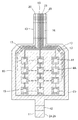
【解決手段】絶縁層10表裏面にセンサパターン14・14Aを形成し、絶縁層表面のセンサパターン14に指を接近させてコンデンサを形成するセンサであって、絶縁層10から伸びる接続用突片13と、センサパターン14・14Aに接続されて絶縁層10から接続用突片13まで伸びる複数のセンサ用導電ライン16と、センサパターン14を包囲して絶縁層10から接続用突片13まで伸びるグランド用導電ライン19と、絶縁層10に積層されてセンサパターン14・14Aを覆う一対のカバー層22・22Aと、絶縁層裏面のカバー層22Aに積層されるグランド層25とを備える。絶縁層10からグランド用接続片11を伸長し、グランド用接続片11の裏面にカバー層22Aとグランド層25の一部24・26を延長積層する。
【選択図】図2
Description
絶縁層から伸びる接続用突片と、センサパターンに接続されて絶縁層から接続用突片まで伸びる複数のセンサ用導電ラインと、絶縁層表面のセンサパターンを包囲して絶縁層から接続用突片まで伸びるグランド用導電ラインと、少なくとも絶縁層に積層されて絶縁層裏面のセンサパターンを覆う絶縁性のカバー層と、このカバー層に積層される導電性のグランド層とを含み、
絶縁層からグランド用接続片を伸ばし、このグランド用接続片の裏面にカバー層とグランド層の一部をそれぞれ延長して積層したことを特徴としている。
また、グランド用接続片の表面に補強層を積層することができる。
また、絶縁層に着脱自在に粘着されて絶縁層表面のセンサパターンを覆う絶縁性のカバー層を備えれば、このカバー層により、絶縁層表面のセンサパターンを保護して傷付くのを未然に防ぐことができる。
2 タッチパッド
4 タッチ板
10 絶縁層
11 グランド用接続片
12 補強層
13 接続用突片
14 センサパターン
14A センサパターン
15 パターン
16 センサ用導電ライン
19 グランド用導電ライン
22 カバー層
22A カバー層
24 カバー層の一部
25 グランド層
26 グランド層の一部
Claims (3)
- 絶縁層の表裏面に導電性のセンサパターンをそれぞれ形成し、絶縁層表面のセンサパターンに導電体を接近させてコンデンサを形成し、センサパターンのどの位置に導電体が存在するかを静電容量の変化として検出する静電容量センサであって、
絶縁層から伸びる接続用突片と、センサパターンに接続されて絶縁層から接続用突片まで伸びる複数のセンサ用導電ラインと、絶縁層表面のセンサパターンを包囲して絶縁層から接続用突片まで伸びるグランド用導電ラインと、少なくとも絶縁層に積層されて絶縁層裏面のセンサパターンを覆う絶縁性のカバー層と、このカバー層に積層される導電性のグランド層とを含み、
絶縁層からグランド用接続片を伸ばし、このグランド用接続片の裏面にカバー層とグランド層の一部をそれぞれ延長して積層したことを特徴とする静電容量センサ。 - 絶縁層に着脱自在に粘着されて絶縁層表面のセンサパターンを覆う絶縁性のカバー層を含んでなる請求項1記載の静電容量センサ。
- グランド用接続片の表面に補強層を積層した請求項1又は2記載の静電容量センサ。
Priority Applications (1)
| Application Number | Priority Date | Filing Date | Title |
|---|---|---|---|
| JP2008131891A JP4999778B2 (ja) | 2008-05-20 | 2008-05-20 | 静電容量センサ |
Applications Claiming Priority (1)
| Application Number | Priority Date | Filing Date | Title |
|---|---|---|---|
| JP2008131891A JP4999778B2 (ja) | 2008-05-20 | 2008-05-20 | 静電容量センサ |
Publications (2)
| Publication Number | Publication Date |
|---|---|
| JP2009283181A true JP2009283181A (ja) | 2009-12-03 |
| JP4999778B2 JP4999778B2 (ja) | 2012-08-15 |
Family
ID=41453446
Family Applications (1)
| Application Number | Title | Priority Date | Filing Date |
|---|---|---|---|
| JP2008131891A Active JP4999778B2 (ja) | 2008-05-20 | 2008-05-20 | 静電容量センサ |
Country Status (1)
| Country | Link |
|---|---|
| JP (1) | JP4999778B2 (ja) |
Cited By (1)
| Publication number | Priority date | Publication date | Assignee | Title |
|---|---|---|---|---|
| JP2018173270A (ja) * | 2013-06-25 | 2018-11-08 | 東芝ライフスタイル株式会社 | 冷蔵庫 |
Citations (5)
| Publication number | Priority date | Publication date | Assignee | Title |
|---|---|---|---|---|
| JPS5790538U (ja) * | 1980-11-25 | 1982-06-03 | ||
| JPH01267916A (ja) * | 1988-04-20 | 1989-10-25 | Matsushita Electric Ind Co Ltd | キー入力装置 |
| JPH11345532A (ja) * | 1998-06-02 | 1999-12-14 | Shin Etsu Polymer Co Ltd | 照光式押釦スイッチ装置 |
| JP2003110207A (ja) * | 2001-09-28 | 2003-04-11 | Alps Electric Co Ltd | フレキシブル基板 |
| JP2003174241A (ja) * | 2001-12-05 | 2003-06-20 | Nec Saitama Ltd | フレキシブルプリント配線板 |
-
2008
- 2008-05-20 JP JP2008131891A patent/JP4999778B2/ja active Active
Patent Citations (5)
| Publication number | Priority date | Publication date | Assignee | Title |
|---|---|---|---|---|
| JPS5790538U (ja) * | 1980-11-25 | 1982-06-03 | ||
| JPH01267916A (ja) * | 1988-04-20 | 1989-10-25 | Matsushita Electric Ind Co Ltd | キー入力装置 |
| JPH11345532A (ja) * | 1998-06-02 | 1999-12-14 | Shin Etsu Polymer Co Ltd | 照光式押釦スイッチ装置 |
| JP2003110207A (ja) * | 2001-09-28 | 2003-04-11 | Alps Electric Co Ltd | フレキシブル基板 |
| JP2003174241A (ja) * | 2001-12-05 | 2003-06-20 | Nec Saitama Ltd | フレキシブルプリント配線板 |
Cited By (1)
| Publication number | Priority date | Publication date | Assignee | Title |
|---|---|---|---|---|
| JP2018173270A (ja) * | 2013-06-25 | 2018-11-08 | 東芝ライフスタイル株式会社 | 冷蔵庫 |
Also Published As
| Publication number | Publication date |
|---|---|
| JP4999778B2 (ja) | 2012-08-15 |
Similar Documents
| Publication | Publication Date | Title |
|---|---|---|
| US8017884B2 (en) | Integrated touch panel and electronic device using the same | |
| US9229591B2 (en) | Touch panel | |
| CN205068342U (zh) | 触摸输入装置 | |
| TWI364579B (ja) | ||
| CN100555868C (zh) | 符合于弧形表面的柔性触摸板传感器网格 | |
| US9084368B2 (en) | Single FPC board for connecting multiple modules and touch sensitive display module using the same | |
| US9083344B2 (en) | Touch sensor with integrated signal bus extensions | |
| US7151227B2 (en) | Electrostatic capacitive touch pad | |
| JP2014071898A (ja) | タッチパネル | |
| CN105278788A (zh) | 触摸输入装置 | |
| JP2010086385A (ja) | 静電容量センサ | |
| WO2016002645A1 (ja) | タッチパネル基板 | |
| JP2013025783A (ja) | タッチパネル | |
| JP2012043054A (ja) | 入力装置 | |
| JP2014071863A (ja) | タッチパネル | |
| JP6264363B2 (ja) | タッチセンサ、タッチパネルおよび電子機器 | |
| TWI374378B (en) | Integrated touch panel and electronic device using the same | |
| TWI517001B (zh) | 觸控模組與電子裝置 | |
| JP4933486B2 (ja) | タッチセンサ | |
| CN106664786B (zh) | 静电浪涌防止构造 | |
| JP4999778B2 (ja) | 静電容量センサ | |
| JP5264839B2 (ja) | センサーシート | |
| CN214751827U (zh) | 一种触摸显示屏和电子设备 | |
| CN104978056A (zh) | 触控面板 | |
| JP2013097457A (ja) | センサーシート |
Legal Events
| Date | Code | Title | Description |
|---|---|---|---|
| A621 | Written request for application examination |
Free format text: JAPANESE INTERMEDIATE CODE: A621 Effective date: 20100524 |
|
| A977 | Report on retrieval |
Free format text: JAPANESE INTERMEDIATE CODE: A971007 Effective date: 20120222 |
|
| A131 | Notification of reasons for refusal |
Free format text: JAPANESE INTERMEDIATE CODE: A131 Effective date: 20120228 |
|
| A521 | Request for written amendment filed |
Free format text: JAPANESE INTERMEDIATE CODE: A523 Effective date: 20120417 |
|
| TRDD | Decision of grant or rejection written | ||
| A01 | Written decision to grant a patent or to grant a registration (utility model) |
Free format text: JAPANESE INTERMEDIATE CODE: A01 Effective date: 20120515 |
|
| A01 | Written decision to grant a patent or to grant a registration (utility model) |
Free format text: JAPANESE INTERMEDIATE CODE: A01 |
|
| A61 | First payment of annual fees (during grant procedure) |
Free format text: JAPANESE INTERMEDIATE CODE: A61 Effective date: 20120515 |
|
| R150 | Certificate of patent or registration of utility model |
Ref document number: 4999778 Country of ref document: JP Free format text: JAPANESE INTERMEDIATE CODE: R150 Free format text: JAPANESE INTERMEDIATE CODE: R150 |
|
| FPAY | Renewal fee payment (event date is renewal date of database) |
Free format text: PAYMENT UNTIL: 20150525 Year of fee payment: 3 |
|
| R250 | Receipt of annual fees |
Free format text: JAPANESE INTERMEDIATE CODE: R250 |
|
| R250 | Receipt of annual fees |
Free format text: JAPANESE INTERMEDIATE CODE: R250 |
|
| R250 | Receipt of annual fees |
Free format text: JAPANESE INTERMEDIATE CODE: R250 |
|
| S531 | Written request for registration of change of domicile |
Free format text: JAPANESE INTERMEDIATE CODE: R313531 |
|
| R350 | Written notification of registration of transfer |
Free format text: JAPANESE INTERMEDIATE CODE: R350 |
|
| R250 | Receipt of annual fees |
Free format text: JAPANESE INTERMEDIATE CODE: R250 |