JP2009298902A - Inorganic phosphor - Google Patents
Inorganic phosphor Download PDFInfo
- Publication number
- JP2009298902A JP2009298902A JP2008154236A JP2008154236A JP2009298902A JP 2009298902 A JP2009298902 A JP 2009298902A JP 2008154236 A JP2008154236 A JP 2008154236A JP 2008154236 A JP2008154236 A JP 2008154236A JP 2009298902 A JP2009298902 A JP 2009298902A
- Authority
- JP
- Japan
- Prior art keywords
- group
- inorganic
- phosphor
- base material
- inorganic phosphor
- Prior art date
- Legal status (The legal status is an assumption and is not a legal conclusion. Google has not performed a legal analysis and makes no representation as to the accuracy of the status listed.)
- Withdrawn
Links
Images

Landscapes
- Electroluminescent Light Sources (AREA)
- Luminescent Compositions (AREA)
Abstract
【課題】新たな発光中心を有し、直流、交流のいずれでも駆動可能な発光素子に適用でき、十分な発光効率が得られ照明用途などで十分な輝度を有し、特に青色で高輝度に発光する無機蛍光体、それを用いる発光素子および直流薄膜型無機EL素子を提供する。
【解決手段】本発明の無機蛍光体は、第2−16族化合物および第12−16族化合物から選ばれる少なくとも1種、またはそれらの混晶を母体材料とする無機蛍光体であって、CuおよびMnを含有せず、周期律表の第6族〜第11族の第2遷移系列に属する金属元素および第3遷移系列に属する金属元素のうちの少なくとも1種と、母体材料を構成する元素以外の第16族元素のうち少なくとも1種とを含有することを特徴とし、発光素子、特に直流薄膜型無機EL素子に好適に用いられる。
【選択図】なしThe present invention is applicable to a light emitting device having a new light emission center and can be driven by either direct current or alternating current, has sufficient luminous efficiency, has sufficient luminance for lighting use, etc., and particularly has high luminance in blue. Provided are an inorganic phosphor that emits light, a light emitting element using the inorganic phosphor, and a direct current thin film inorganic EL element.
An inorganic phosphor according to the present invention is an inorganic phosphor having at least one selected from a group 2-16 compound and a group 12-16 compound, or a mixed crystal thereof as a base material. And Mn, and at least one of the metal elements belonging to the second transition series of Groups 6 to 11 of the periodic table and the metal elements belonging to the third transition series, and an element constituting the base material It contains at least 1 sort (s) among group 16 elements other than these, and is used suitably for a light emitting element, especially a direct current thin film type inorganic EL element.
[Selection figure] None
Description
本発明は、交流分散型無機EL素子、交流薄膜型無機EL素子、直流薄膜型無機EL素子等に有用な無機蛍光体(以下、無機蛍光体材料ともいう)に関するものである。 The present invention relates to an inorganic phosphor (hereinafter also referred to as an inorganic phosphor material) useful for an AC dispersion type inorganic EL element, an AC thin film type inorganic EL element, a DC thin film type inorganic EL element, and the like.
蛍光体とは、外部から光、電気、圧力、熱、電子線等のエネルギーが与えられることによって発光する材料のことであり、古くから知られている材料である。中でも無機材料から成る蛍光体は、その発光特性や安定性などからブラウン管、蛍光ランプ、エレクトロルミネッセンス(EL)素子等に用いられてきた。近年ではLED用の色変換材料として、PDPといった低速電子線励起用としても盛んに研究がなされている。 A phosphor is a material that emits light when given energy such as light, electricity, pressure, heat, and electron beam from the outside, and has been known for a long time. Among them, phosphors made of inorganic materials have been used for cathode ray tubes, fluorescent lamps, electroluminescence (EL) elements, and the like because of their light emission characteristics and stability. In recent years, as a color conversion material for LEDs, active research has been made for low-energy electron beam excitation such as PDP.
無機蛍光体を用いたエレクトロルミネッセンス(EL)素子は、駆動方法によって交流駆動型と直流駆動型に大別される。交流駆動型の中には高誘電性バインダーに蛍光体粒子を分散してなる交流分散型EL素子、誘電体層間に蛍光体薄膜を挟んでなる交流薄膜型EL素子の2種類があり、直流駆動型の中には、透明電極と金属電極で蛍光体薄膜を挟んで低電圧直流駆動する直流薄膜型EL素子がある。 Electroluminescence (EL) elements using inorganic phosphors are roughly classified into an AC driving type and a DC driving type depending on the driving method. There are two types of AC drive type: an AC dispersion type EL element in which phosphor particles are dispersed in a high dielectric binder, and an AC thin film type EL element in which a phosphor thin film is sandwiched between dielectric layers. Among the molds, there is a direct current thin film type EL element that is driven by a low voltage direct current with a phosphor thin film sandwiched between a transparent electrode and a metal electrode.
次に直流駆動型無機EL素子を取り上げて説明する。
直流駆動型無機EL素子は、1970〜80年代に研究が盛んになされていた(非特許文献1)。これはZnSe:MnをGaAs基板上にMBEにより成膜し、Au電極と挟むことで構成される素子である。約4Vを印加することで電極からトンネル効果で電子が注入され、発光中心であるMnを励起し、発光するという機構である。しかしながら、この素子は発光効率が低いこと(〜0.05lm/W)、再現性が低いことから、それ以来、実用化はもとより学術的な研究もなされていない。
Next, a direct-current drive type inorganic EL element will be taken up and described.
Research on the direct-current drive type inorganic EL element was actively made in the 1970s and 1980s (Non-patent Document 1). This is an element formed by depositing ZnSe: Mn on a GaAs substrate by MBE and sandwiching it with an Au electrode. By applying about 4 V, electrons are injected from the electrode by the tunnel effect, and Mn which is the emission center is excited to emit light. However, since this device has low luminous efficiency (˜0.05 lm / W) and low reproducibility, it has not been put into practical use or studied academically since then.
近年、新たな直流駆動型無機EL素子が報告された(特許文献1)。発光材料としては、CuやMnといった従来から知られている発光中心を含有するZnS系であり、これを透明電極であるITO電極と背面電極であるAg電極とで挟みこんだ構成である。その発光機構については記載されていないが、想定される機構としては、Cuとともに含有するClとでDAペア対を形成し、そこで注入された電子と正孔の再結合すなわち発光すると考えられる。 In recent years, a new direct-current drive type inorganic EL element has been reported (Patent Document 1). The light-emitting material is a ZnS-based material containing a conventionally known light emission center such as Cu or Mn, and has a configuration in which this is sandwiched between an ITO electrode as a transparent electrode and an Ag electrode as a back electrode. Although the light emission mechanism is not described, it is considered that a DA pair pair is formed with Cl contained together with Cu, and recombination of electrons and holes injected therein, that is, light emission.
同様な駆動方法で発光する有機EL素子と比較して、発光素子がすべて無機材料で構成されているため、耐久性が高く、照明やディスプレイなど様々な分野での活用が可能となる。さらに同様な駆動であるLEDはすべて無機材料で構成されているという点で類似しているが、LEDは発光面積が極微小すなわち点発光であるため、単位面積あたりの輝度は高いものの、絶対光量(光束)は少ないために、用途が限られる。一方無機EL素子はもともと面発光であるため、多くの光束を得ることが可能であるという点で有利である。 Compared with an organic EL element that emits light by a similar driving method, the light-emitting elements are all made of an inorganic material, so that they have high durability and can be used in various fields such as lighting and displays. Furthermore, LEDs that are driven in a similar manner are similar in that they are all composed of an inorganic material. However, since LEDs have a very small emission area, that is, point emission, the luminance per unit area is high, but the absolute light quantity Since there are few (light beams), a use is limited. On the other hand, an inorganic EL element is naturally surface emitting, which is advantageous in that a large amount of light can be obtained.
また、特許文献2は、付活剤として銅を含み、共付活剤として塩素および臭素から選ばれる少なくとも1種類を含み、かつ、第6族から第10族までの第2遷移系列または第3遷移系列に属する金属元素の少なくとも1種類を含有する硫化亜鉛粒子からなる無機蛍光体を、特許文献3は、硫化亜鉛を母体として、付活剤として銅、第1の共付活剤として塩素、臭素の少なくとも1種、第2の共付活剤として金を含有する蛍光体材料を、それぞれ開示している。
また、特許文献4は、希土類硫化物を母体材料とし、該母体材料とPr、Mn、Auを含み、該母体材料を活性化する活性化剤との混合物を生成し、生成した混合物を加熱して該母体材料を活性化する発光体の製造方法を開示している。
Patent Document 4 uses rare earth sulfide as a base material, generates a mixture of the base material and an activator containing Pr, Mn, Au and activates the base material, and heats the generated mixture. Thus, a method for manufacturing a light emitter that activates the base material is disclosed.
しかしながら、特許文献1の直流駆動無機EL素子は発光効率が低く、実用的ではなかった。また、特許文献2および特許文献3に記載の蛍光体は、付活剤として銅を含んでいることから、DA(ドナーアクセプタ)ペア発光型のものであるが、粒子分散型および交流薄膜型にしか適用できず、用途が限定されるという問題があった。さらに、特許文献4に記載の発光体は、母体材料として希土類硫化物を用いたMn及び/またはPrの局在発光型と考えられるが、Mnや希土類の局在発光型のものは、直流、交流のいずれでも駆動可能な発光素子に適用できるが、十分な発光効率が得られないという問題があった。
また、特許文献1〜4のいずれの蛍光体も照明用途などで十分な輝度を有するものではなく、特に青色で高輝度に発光するものはなかった。
However, the direct current drive inorganic EL element of
In addition, none of the phosphors of
以上のことから、新たな発光中心を有し、直流、交流のいずれでも駆動可能な発光素子に適用でき、十分な発光効率が得られ、照明用途などで十分な輝度を有し、特に青色で高輝度に発光する蛍光体の開発が望まれていた。
従って、本願発明は、新たな発光中心を有し、直流、交流のいずれでも駆動可能な発光素子に適用でき、十分な発光効率が得られ照明用途などで十分な輝度を有し、特に青色で高輝度に発光する無機蛍光体、それを用いる発光素子および直流薄膜型無機EL素子を提供しようとするものである。
From the above, it can be applied to a light emitting device that has a new light emission center and can be driven by either direct current or alternating current, has sufficient light emission efficiency, has sufficient luminance for lighting use, etc. Development of a phosphor that emits light with high brightness has been desired.
Therefore, the present invention can be applied to a light emitting element having a new light emission center and can be driven by either direct current or alternating current, has sufficient light emission efficiency, has sufficient luminance for lighting use, etc. An object of the present invention is to provide an inorganic phosphor that emits light with high brightness, a light emitting element using the inorganic phosphor, and a direct current thin film type inorganic EL element.
発明者らは、鋭意検討の結果、従来から知られているCuやMnや希土類といった発光中心金属を添加せずに、周期律表の第6族〜第11族までの第2遷移系列に属する金属元素または第3遷移系列に属する金属元素、及び、母体材料を構成する元素以外の元素で周期律表の第16族に属する元素を第2−16族化合物に添加することによって、紫外線励起でのフォトルミネッセンスおよび直流駆動によるエレクトロルミネッセンスを示す新規な蛍光体を見出したことにより、本発明を成すに至った。 As a result of intensive studies, the inventors belong to the second transition series from Group 6 to Group 11 of the periodic table without adding conventionally known luminescent center metals such as Cu, Mn, and rare earths. By adding a metal element or a metal element belonging to the third transition series and an element other than the element constituting the base material belonging to the group 16 of the periodic table to the group 2-16 compound, by ultraviolet excitation. The present inventors have found a novel phosphor exhibiting photoluminescence and electroluminescence by direct current drive.
即ち、本発明は以下の要件により達成される。
(1)第2−16族化合物および第12−16族化合物から選ばれる少なくとも1種、またはそれらの混晶を母体材料とする無機蛍光体であって、CuおよびMnを含有せず、周期律表の第6族〜第11族の第2遷移系列に属する金属元素および第3遷移系列に属する金属元素のうちの少なくとも1種と、母体材料を構成する元素以外の第16族元素のうち少なくとも1種とを含有することを特徴とする無機蛍光体。
(2)前記第6族〜第11族の第2遷移系列に属する元素または第3遷移系列に属する元素が、Ru、Rh、Pd、Ag、Os、Ir、PtおよびAuのうちの少なくとも1種であることを特徴とする前記(1)の無機蛍光体。
(3)前記母体材料が硫化亜鉛、セレン化亜鉛もしくはその混晶からなることを特徴とする前記(1)の無機蛍光体。
(4)前記母体材料を構成する元素以外の第16族元素が酸素であることを特徴とする前記(3)の無機蛍光体。
(5)周期律表の第13族および第15族に属する元素から選ばれる少なくとも1種類の元素を含有することを特徴とする前記(1)の無機蛍光体。
(6)前記(1)〜(5)のいずれかに記載の無機蛍光体を有する発光素子。
(7)前記(1)〜(5)のいずれかに記載の無機蛍光体を有する直流薄膜型無機EL素子。
(8)p型半導体層を有する前記(7)の直流薄膜型無機EL素子。
That is, the present invention is achieved by the following requirements.
(1) An inorganic phosphor having as a base material at least one selected from Group 2-16 compounds and Group 12-16 compounds, or a mixed crystal thereof, which does not contain Cu and Mn, and has a periodic rule At least one of the metal elements belonging to the second transition series of Group 6 to Group 11 of the table and the metal elements belonging to the third transition series, and at least of the Group 16 elements other than the elements constituting the
(2) The element belonging to the second transition series of Group 6 to Group 11 or the element belonging to the third transition series is at least one of Ru, Rh, Pd, Ag, Os, Ir, Pt, and Au. (1) The inorganic phosphor as described above.
(3) The inorganic phosphor according to (1), wherein the base material is composed of zinc sulfide, zinc selenide or a mixed crystal thereof.
(4) The inorganic phosphor according to (3) above, wherein the group 16 element other than the elements constituting the host material is oxygen.
(5) The inorganic phosphor according to (1) above, which contains at least one element selected from elements belonging to Groups 13 and 15 of the periodic table.
(6) A light emitting device having the inorganic phosphor according to any one of (1) to (5).
(7) A direct-current thin film inorganic EL element having the inorganic phosphor according to any one of (1) to (5).
(8) The direct current thin film inorganic EL element according to (7), which has a p-type semiconductor layer.
本発明の無機蛍光体は、これまでにない新たな発光中心による強度の高い青色発光を示すだけでなく、無機エレクトロルミネッセンス素子用の蛍光体として有用であり、発光輝度に優れ長寿命を有するものである。 The inorganic phosphor of the present invention not only exhibits high-intensity blue light emission due to a new emission center that has never been seen before, but is also useful as a phosphor for inorganic electroluminescent elements, and has excellent emission luminance and long life. It is.
以下本発明について詳しく説明する。
本発明の無機蛍光体は、第2−16族化合物または第12−16族化合物から選ばれる少なくとも1種、またはそれらの混晶を母体材料とし、さらに周期律表の第6族〜第11族の第2遷移系列に属する金属元素および第3遷移系列に属する金属元素のうちの少なくともいずれかと、母体材料を構成する元素以外の第16族元素のうち少なくとも1種とを含有することを特徴とする。
The present invention will be described in detail below.
The inorganic phosphor of the present invention has at least one selected from Group 2-16 compounds or Group 12-16 compounds, or a mixed crystal thereof as a base material, and further includes Groups 6 to 11 of the periodic table. And at least one of a metal element belonging to the second transition series and a metal element belonging to the third transition series, and at least one of group 16 elements other than the elements constituting the base material, To do.
なお、本発明の無機蛍光体の母体材料として用いられる、第2−16族化合物とは、周期律表の第2族に属する少なくとも1種の元素と周期律表の第16族に属する少なくとも1種の元素からなる化合物、第12−16族化合物とは、周期律表の第12族に属する少なくとも1種の元素と周期律表の第16族に属する少なくとも1種の元素からなる化合物を意味するものであり、本発明の属する技術分野における通常の知識を有するもの(当業者)が通常使用している標記・表現である。
該母体材料の例としては、ZnS、ZnSe、ZnTe、CdS、CdSe、CdTe、CaS、SrS、BaSなどの第2−16族化合物または第12−16族化合物から選ばれる少なくとも1種またはそれらの混晶が用いられる。好ましくはZnS、ZnSe、ZnSSe、SrS、CaS、SrSe、SrSSeであり、さらに好ましくは、ZnS、ZnSe、ZnSSeである。
また母体材料とは、蛍光体材料を構成する化合物のうち1モル%以上を構成する材料すべてを指す。例えばZnSとZnSeとの比率が99モル%と1モル%の場合はZnSSe混晶を母体材料とみなし、99.1モル%と0.9モル%の場合はZnS単体を母体材料と考える。
The Group 2-16 compound used as the base material of the inorganic phosphor of the present invention is at least one element belonging to
Examples of the base material include at least one selected from Group 2-16 compounds such as ZnS, ZnSe, ZnTe, CdS, CdSe, CdTe, CaS, SrS, BaS, and the like, or a mixture thereof. Crystals are used. ZnS, ZnSe, ZnSSe, SrS, CaS, SrSe, SrSSe are preferable, and ZnS, ZnSe, ZnSSe are more preferable.
The base material refers to all materials constituting 1 mol% or more of the compounds constituting the phosphor material. For example, when the ratio of ZnS to ZnSe is 99 mol% and 1 mol%, the ZnSSe mixed crystal is regarded as a base material, and when 99.1 mol% and 0.9 mol%, ZnS simple substance is considered as the base material.
本発明の無機蛍光体に用いられる、周期律表の第6族〜第11族の第2遷移系列に属する金属元素および第3遷移系列に属する金属元素の例としては、Mo、Tc、Ru、Rh、Pd、Ag、W、Re、Os、Ir、Pt、Auがあるが、中でもRu、Pd、Ag、Os、Ir、Pt、Auが好ましいが、さらにはOs、Ir、Pt、Auが好ましい。これらの金属は単独で含有していてもよいし、複数で含有していてもよい。 Examples of metal elements belonging to the second transition series of Groups 6 to 11 of the periodic table and metal elements belonging to the third transition series used in the inorganic phosphor of the present invention include Mo, Tc, Ru, There are Rh, Pd, Ag, W, Re, Os, Ir, Pt, and Au. Among them, Ru, Pd, Ag, Os, Ir, Pt, and Au are preferable, and Os, Ir, Pt, and Au are more preferable. . These metals may be contained alone or in plural.
上記の周期律表の第6族〜第11族の第2遷移系列に属する金属元素および第3遷移系列に属する金属元素の母体材料への含有のさせ方、すなわちドープ方法は、いかなる方法にも限定するものではないが、たとえば、焼成での粒子形成時の金属塩の形で混入させても良いし、焼成条件で溶融、昇華もしくは反応可能であれば、化合物結晶の形で混入させても良い。これらの金属は母体材料の結晶内に取り込まれた部分以外の結晶表面への析出分や、結晶表面への吸着分は、エッチングや洗浄等で除去することが好ましい。金属塩としては、酸化物、硫化物、硫酸化物、シュウ酸化物、ハロゲン化物、硝酸化物、窒化物等、いかなる化合物でも良いが、中でも酸化物、硫化物、ハロゲン化物が好ましく用いられる。それぞれ単独で用いても良いが、複数種の金属塩を用いても良い。ドープ量としては、母体材料1モルに対して1×10⁻⁷モル以上1×10⁻²モル未満が好ましく、さらに好ましくは1×10⁻⁵モル以上5×10⁻³モル未満である。 Any method may be used for adding a metal element belonging to the second transition series of Group 6 to Group 11 of the above periodic table and a metal element belonging to the third transition series to the base material, that is, a doping method. Although it is not limited, for example, it may be mixed in the form of a metal salt at the time of particle formation by firing, or may be mixed in the form of a compound crystal if it can be melted, sublimated or reacted under firing conditions. good. These metals are preferably removed by etching, washing or the like on the crystal surface other than the portion taken into the crystal of the base material and on the crystal surface. The metal salt may be any compound such as oxide, sulfide, sulfate, oxide, halide, nitrate, nitride, etc. Among them, oxide, sulfide, and halide are preferably used. Each may be used alone, but a plurality of types of metal salts may be used. The dope amount is preferably 1 × 10 −7 mol or more and less than 1 × 10 −2 mol, more preferably 1 × 10 −5 mol or more and less than 5 × 10 −3 mol, relative to 1 mol of the base material.
本発明の無機蛍光体に用いられる、母体材料を構成する元素以外の第16族元素の例としては、母体材料が硫黄化合物の場合はO、Se、Teであり、セレン化号物の場合はO、S、Teであり、硫黄とセレンの混晶化合物の場合は、O、Teである。これらの元素は単独で含有していても良いし、複数で含有していても良い。特に母体化合物が硫黄化合物の場合、結晶構造中の硫黄欠陥を生成しやすいために、同族の−2価の元素を含有させることで、発光に対して効率低下を引き起こす結晶欠陥の生成を抑制し、発光効率を高めることができる。Irといった第6族〜第11族の第2遷移系列に属する金属元素を含有するZnSでは、Ir周囲の局所的な結晶構造の歪みをSだけでは埋めることができず、イオン半径の大きなSeやイオン半径の小さなOで格子位置を占めることができるため、結晶欠陥を低減でき、結果として顕著な発光効率の増大が得られる。 Examples of Group 16 elements other than those constituting the host material used in the inorganic phosphor of the present invention include O, Se, and Te when the host material is a sulfur compound, and in the case of selenide In the case of a mixed crystal compound of sulfur and selenium, they are O and Te. These elements may be contained singly or plurally. In particular, when the base compound is a sulfur compound, sulfur defects in the crystal structure are likely to be generated. Therefore, by adding a homovalent -2 element, the generation of crystal defects that cause a reduction in efficiency with respect to light emission is suppressed. , Luminous efficiency can be increased. In ZnS containing a metal element belonging to the second transition series of Group 6 to Group 11, such as Ir, the distortion of the local crystal structure around Ir cannot be filled with S alone, and Se having a large ionic radius can be obtained. Since the lattice position can be occupied by O having a small ion radius, crystal defects can be reduced, and as a result, a remarkable increase in luminous efficiency can be obtained.
上記の母体材料を構成する元素以外の第16族元素の母体材料への含有のさせ方、すなわちドープ方法は、前述の周期律表の第6族〜第11族の第2遷移系列に属する金属元素および第3遷移系列に属する金属元素の母体材料への含有のさせ方と同様に、いかなる方法にも限定するものではないが、たとえば、前述の第6族〜第11族の第2遷移系列に属する金属元素および第3遷移系列に属する金属元素の母体材料へ含有させるために用いる金属塩として酸化物や硫化物、セレン化物、テルル化物を用いたり、母体材料の酸化物や硫化物、セレン化物、テルル化物を用いることで、母体材料を構成する元素以外の第16族元素をドープさせることができる。また焼成条件で溶融、昇華もしくは反応可能であれば、化合物結晶の形で混入させても良い。さらに、酸素や硫黄やセレンについては、焼成雰囲気として分圧をコントロールすることでドープしても良い。これらの元素は母体材料の結晶内に取り込まれた部分以外の結晶表面への析出分や、結晶表面への吸着分は、エッチングや洗浄等で除去することが好ましい。ドープ量としては、母体材料1モルに対して1×10⁻⁷モル以上1×10⁻²モル未満が好ましく、さらに好ましくは1×10−5モル以上5×10−3モル未満である。 The method of incorporating the group 16 element other than the elements constituting the matrix material into the matrix material, that is, the doping method, is a metal belonging to the second transition series of groups 6 to 11 of the periodic table. The method is not limited to any method, as is the case with the inclusion of the element and the metal element belonging to the third transition series into the base material. For example, the above-mentioned second transition series of Group 6 to Group 11 are not limited. As the metal salt used for inclusion in the base material of the metal element belonging to the group 3 and the metal element belonging to the third transition series, an oxide, sulfide, selenide, telluride is used, or the base material oxide, sulfide, selenium By using a compound or telluride, a group 16 element other than the elements constituting the base material can be doped. Further, if it can be melted, sublimated or reacted under firing conditions, it may be mixed in the form of compound crystals. Further, oxygen, sulfur, and selenium may be doped by controlling the partial pressure as a firing atmosphere. These elements are preferably removed by etching, washing, or the like, on the crystal surface other than the portion taken into the crystal of the host material and on the crystal surface. The doping amount is preferably 1 × 10 −7 mol or more and less than 1 × 10 −2 mol, more preferably 1 × 10 −5 mol or more and less than 5 × 10 −3 mol, relative to 1 mol of the base material.
さらに蛍光体として性能を上げるために、周期律表の第13族に属する元素及び第15族に属する元素から選ばれる少なくとも1種の元素を含有することが有効である。
好ましくは、第13族に属する元素から選ばれる少なくとも1種の元素と、第15族に属する元素から選ばれる少なくとも1種の元素とを含有し、さらに好ましくは、第13族に属する元素としてAl、Ga、InおよびTlから選ばれる少なくとも1種を含有し、第15族に属する元素としてN、P、Sb、AsおよびBiから選ばれる少なくとも1種を含有し、特に好ましくは、第13族に属する元素としてGaを含有し、第15族に属する元素としてN、PおよびSbから選ばれる少なくとも1種を含有する。
また、これらの元素を蛍光体に含有させる場合には、第13族に属する元素と第15族に属する元素とからなる化合物(第13−15族化合物)を添加することが好ましい。
これらの周期律表の第13族に属する元素及び第15族に属する元素から選ばれる少なくとも1種の元素の含有量は、特に限定されないが、母体材料1モルに対して1×10⁻⁷モル以上1×10⁻²未満が好ましい。
Further, in order to improve the performance as a phosphor, it is effective to contain at least one element selected from elements belonging to Group 13 and elements belonging to Group 15 of the periodic table.
Preferably, it contains at least one element selected from elements belonging to Group 13, and at least one element selected from elements belonging to Group 15, and more preferably Al as an element belonging to Group 13 And at least one selected from Ga, In and Tl, and at least one selected from N, P, Sb, As and Bi as an element belonging to Group 15, and particularly preferably in Group 13 Ga is contained as an element belonging, and at least one selected from N, P and Sb is contained as an element belonging to Group 15.
In addition, when these elements are contained in the phosphor, it is preferable to add a compound composed of an element belonging to Group 13 and an element belonging to Group 15 (Group 13-15 compound).
The content of at least one element selected from the elements belonging to Group 13 and the elements belonging to Group 15 of these periodic tables is not particularly limited, but is 1 × 10 −7 mol with respect to 1 mol of the base material. Above, less than 1 × 10 −2 is preferable.
一般に交流駆動の無機EL素子は電圧50〜300V、周波数50〜5000Hzで駆動するが、直流駆動の無機EL素子は0.1〜20Vと低電圧で駆動できることが特長として挙げられる。本発明の無機蛍光体は、分散型無機EL素子、薄膜型無機EL素子といった交流駆動型素子、さらには直流駆動型の無機EL素子に有用であるが、中でも直流駆動型無機EL素子に有用である。
次に直流駆動型無機EL素子について詳しく説明する。
直流駆動型無機EL素子は少なくとも透明電極(透明導電膜とも称する)と蛍光体層(発光層とも称する)と背面電極とから構成される。発光層の厚みは厚くなりすぎると発光に必要な電界強度を得るために両電極間の電圧が上昇するので、低電圧駆動を実現するためには50μm以下が好ましく、さらに好ましくは30μm以下である。また厚みが薄くなりすぎると、蛍光体層の両面にある電極が短絡しやすくなるため、短絡を避けるために厚みは50nm以上が好ましく、さらに好ましくは100nm以上である。
また透明電極と蛍光体層もしくは蛍光体層と背面電極の間にp型半導体層を設けることで発光強度を高めることができる。p型半導体層を構成する材料は、正孔をキャリアとする硫化物の材料である。例えば、硫化銅(Cu2S)、あるいは硫化亜鉛(ZnS)と硫化銅の混合物を用いることができる。また、ZnSにアクセプターとなる不純物元素であるリチウム(Li)、カリウム(K)、ルビジウム(Rb)、セシウム(Cs)、アルミニウム(Al)、ガリウム(Ga)、又はインジウム(In)をドープしたものを用いることもできる。さらに、ZnSにCu、又はAgを過剰にドープしたものを用いることもできる。
In general, an AC driven inorganic EL element is driven at a voltage of 50 to 300 V and a frequency of 50 to 5000 Hz, but a DC driven inorganic EL element can be driven at a low voltage of 0.1 to 20 V. The inorganic phosphor of the present invention is useful for an AC drive type element such as a dispersion type inorganic EL element and a thin film type inorganic EL element, and also for a DC drive type inorganic EL element. is there.
Next, the direct current drive type inorganic EL element will be described in detail.
The direct current drive type inorganic EL element includes at least a transparent electrode (also referred to as a transparent conductive film), a phosphor layer (also referred to as a light emitting layer), and a back electrode. If the thickness of the light emitting layer becomes too thick, the voltage between both electrodes rises in order to obtain the electric field strength necessary for light emission. Therefore, in order to realize low voltage driving, it is preferably 50 μm or less, more preferably 30 μm or less. . If the thickness is too thin, the electrodes on both sides of the phosphor layer are easily short-circuited. Therefore, the thickness is preferably 50 nm or more, more preferably 100 nm or more in order to avoid a short circuit.
Further, the emission intensity can be increased by providing a p-type semiconductor layer between the transparent electrode and the phosphor layer or between the phosphor layer and the back electrode. The material constituting the p-type semiconductor layer is a sulfide material using holes as carriers. For example, copper sulfide (Cu 2 S) or a mixture of zinc sulfide (ZnS) and copper sulfide can be used. Also, ZnS doped with acceptor elements such as lithium (Li), potassium (K), rubidium (Rb), cesium (Cs), aluminum (Al), gallium (Ga), or indium (In) Can also be used. Further, ZnS excessively doped with Cu or Ag can also be used.
成膜方法としては、物理的蒸着法である抵抗加熱蒸着法や電子ビーム蒸着、スパッタリングやイオンプレーティング、CVD(Chemical Vapor Deposition)など無機材料を一般的に成膜する方法が用いられる。本発明に用いられる蛍光体は高温でも安定で高融点であることから、高融点材料を蒸着するのに適した電子ビーム蒸着法や、蒸着源をターゲット化できる場合はスパッタリング法が好適に用いられる。さらに電子ビーム蒸着の場合、蛍光体中に含有する金属の蒸気圧が、母体材料の蒸気圧と大幅に異なる場合には、それぞれ単独の蒸着源として複数の蒸着源を利用した蒸着方法も有用である。また結晶性を高めるという意味で、基板との格子マッチングを考慮したMBE(Molecular Beam Epitaxiy)法も好適である。 As a film forming method, a physical heating method such as resistance heating evaporation, electron beam evaporation, sputtering, ion plating, CVD (Chemical Vapor Deposition), or the like is generally used. Since the phosphor used in the present invention is stable and has a high melting point even at a high temperature, an electron beam vapor deposition method suitable for depositing a high melting point material or a sputtering method is suitably used when the deposition source can be targeted. . Furthermore, in the case of electron beam evaporation, if the vapor pressure of the metal contained in the phosphor is significantly different from the vapor pressure of the host material, an evaporation method using multiple evaporation sources as individual evaporation sources is also useful. is there. In order to enhance crystallinity, an MBE (Molecular Beam Epitaxy) method considering lattice matching with the substrate is also suitable.
本発明に好ましく用いられる透明導電膜の表面抵抗率は、10Ω/□以下であることが好ましく、0.01Ω/□〜10Ω/□が更に好ましい。特に0.01Ω/□〜1Ω/□が好ましい。
透明導電膜の表面低効率は、JIS K6911に記載の方法に準じて測定することができる。
透明導電膜は、ガラス又はプラスチック基板上に形成されており、かつ酸化錫を含有していることが好ましい。
The surface resistivity of the transparent conductive film preferably used in the present invention is preferably 10Ω / □ or less, more preferably 0.01Ω / □ to 10Ω / □. In particular, 0.01Ω / □ to 1Ω / □ is preferable.
The surface low efficiency of the transparent conductive film can be measured according to the method described in JIS K6911.
The transparent conductive film is preferably formed on a glass or plastic substrate and contains tin oxide.
すなわち、ガラスとしては無アルカリガラス、ソーダライムガラスなど、一般的なガラスが用いられるが、耐熱性が高く平坦性の高いガラスを用いることが好ましい。プラスチック基板としては、ポリエチレンテレフタレートやポリエチレンナフタレート、トリアセチルセルロースベース等の透明フィルムが好適に用いられる。それらを基板として、インディウム・錫酸化物(ITO)や錫酸化物、酸化亜鉛等の透明導電性物質を蒸着、塗布、印刷等の方法で付着、成膜することができる。
この場合、耐久性を上げる目的で透明導電膜表面を酸化錫を主体の層とすることが好ましい。
That is, as glass, general glass such as alkali-free glass or soda lime glass is used, but it is preferable to use glass having high heat resistance and high flatness. As the plastic substrate, a transparent film such as polyethylene terephthalate, polyethylene naphthalate, or triacetyl cellulose base is preferably used. Using these as a substrate, a transparent conductive material such as indium tin oxide (ITO), tin oxide, or zinc oxide can be deposited and formed by a method such as vapor deposition, coating, or printing.
In this case, it is preferable that the surface of the transparent conductive film is mainly composed of tin oxide for the purpose of increasing durability.
透明導電膜を構成する透明導電性物質の好ましい付着量は、透明導電膜に対して、100質量%〜1質量%、より好ましくは、70質量%〜5質量%、さらに好ましくは、40質量%〜10質量%である。
透明導電膜の調製法はスパッター、真空蒸着等の気相法であっても良い。ペースト状のITOや酸化錫を塗布やスクリーン印刷で作成したり、膜全体を加熱したりレーザーにて加熱して成膜しても良い。
本発明のEL素子において、透明導電膜には一般的に用いられる任意の透明電極材料が用いられる。例えば錫ドープ酸化錫、アンチモンドープ酸化錫、亜鉛ドープ酸化錫、フッ素ドープ酸化錫、酸化亜鉛などの酸化物、銀の薄膜を高屈折率層で挟んだ多層構造、ポリアニリン、ポリピロールなどの共役系高分子などが挙げられる。
The preferable adhesion amount of the transparent conductive material constituting the transparent conductive film is 100% by mass to 1% by mass, more preferably 70% by mass to 5% by mass, and still more preferably 40% by mass with respect to the transparent conductive film. -10 mass%.
The method for preparing the transparent conductive film may be a gas phase method such as sputtering or vacuum deposition. Paste-like ITO or tin oxide may be formed by coating or screen printing, or the whole film may be heated or heated with a laser to form a film.
In the EL device of the present invention, any transparent electrode material that is generally used is used for the transparent conductive film. For example, tin-doped tin oxide, antimony-doped tin oxide, zinc-doped tin oxide, fluorine-doped tin oxide, zinc oxide and other oxides, a multilayer structure in which a silver thin film is sandwiched between high refractive index layers, polyaniline, polypyrrole and other conjugated systems Examples include molecules.
更に低抵抗化するには、例えば櫛型あるいはグリッド型等の網目状ないしストライプ状金属細線を配置して通電性を改善することが好ましい。金属や合金の細線としては、銅や銀、アルミニウム、ニッケル等が好ましく用いられる。この金属細線の太さは、任意であるが、0.5μm程度から20μmの間が好ましい。金属細線は、50μm〜400μmの間隔のピッチで配置されていることが好ましく、特に100μm〜300μmピッチが好ましい。金属細線を配置することで、光の透過率が減少するが、この減少は出来るだけ小さいことが重要で、80%以上100%未満の透過率を確保することが好ましい。 In order to further reduce the resistance, it is preferable to improve the conductivity by arranging, for example, a comb-shaped or grid-shaped mesh or stripe-shaped fine metal wire. Copper, silver, aluminum, nickel, or the like is preferably used as the metal or alloy thin wire. The thickness of the fine metal wire is arbitrary, but is preferably between about 0.5 μm and 20 μm. The fine metal wires are preferably arranged at a pitch of 50 μm to 400 μm, and a pitch of 100 μm to 300 μm is particularly preferable. Although the light transmittance is reduced by arranging the fine metal wires, it is important that this reduction is as small as possible, and it is preferable to secure a transmittance of 80% or more and less than 100%.
金属細線は、メッシュを透明導電性フィルムに張り合わせてもよいし、予めマスク蒸着ないしエッチングによりフィルム上に形成した金属細線上に金属酸化物等を塗布、蒸着しても良い。また、予め形成した金属酸化物薄膜上に上記の金属細線を形成してもよい。
これとは、異なる方法となるが、金属細線の代わりに、100nm以下の平均厚みを有する金属薄膜を金属酸化物と積層して本発明に適した透明導電膜とすることができる。金属薄膜に用いられる金属としては、AuやIn、Sn、Cu、Niなど耐腐食性が高く、展延性等に優れたものが好ましいが、特にこの限りではない。
これらの複層膜は、高い光透過率を実現することが好ましく、具体的には70%以上の光透過率を有することが好ましく、80%以上の光透過率を有することが特に好ましい。光透過率を規定する波長は、550nmである。
光の透過率に関しては、干渉フィルターを用いて550nmの単色光を取り出し、一般に用いられる白色光源を用いた積分型光量測定やスペクトル測定装置を用いて測定することが出来る。
For the fine metal wires, the mesh may be bonded to the transparent conductive film, or a metal oxide or the like may be applied and vapor-deposited on the fine metal wires previously formed on the film by mask vapor deposition or etching. Moreover, you may form said metal fine wire on the metal oxide thin film formed previously.
Although this is a different method, a transparent conductive film suitable for the present invention can be obtained by laminating a metal thin film having an average thickness of 100 nm or less with a metal oxide instead of a thin metal wire. The metal used for the metal thin film is preferably a metal having high corrosion resistance such as Au, In, Sn, Cu, and Ni and excellent in spreadability, but is not particularly limited thereto.
These multilayer films preferably realize high light transmittance, specifically, preferably have a light transmittance of 70% or more, and particularly preferably have a light transmittance of 80% or more. The wavelength that defines the light transmittance is 550 nm.
Regarding the light transmittance, monochromatic light of 550 nm can be taken out using an interference filter, and can be measured using an integral light quantity measurement or a spectrum measuring apparatus using a commonly used white light source.
(背面電極)
光を取り出さない側の背面電極は、導電性の有る任意の材料が使用出来る。金、銀、白金、銅、鉄、アルミニウムなどの金属、グラファイトなどの中から、作製する素子の形態、作製工程の温度等により適時選択されるが、その中でも熱伝導率が高いことが重要で、2.0W/cm・deg以上であることが好ましい。
また、EL素子の周辺部に高い放熱性と通電性を確保するために、金属シートや金属メッシュを用いることも好ましい。
(Back electrode)
For the back electrode on the side from which light is not extracted, any conductive material can be used. It is selected from gold, silver, platinum, copper, iron, aluminum and other metals, graphite, etc., depending on the form of the device to be produced, the temperature of the production process, etc., among which it is important that the thermal conductivity is high. 2.0 W / cm · deg or more is preferable.
It is also preferable to use a metal sheet or a metal mesh in order to ensure high heat dissipation and electrical conductivity in the periphery of the EL element.
本発明に利用可能な無機蛍光体は、当業界で広く用いられる焼成法(固相法)で形成することができる。例えば、硫化亜鉛の場合、液相法で10nm〜50nmの微粒子粉末(生粉と呼ぶ)を作成し、これを一次粒子として用い、これに付活剤と呼ばれる不純物を混入させて融剤とともに坩堝にて900℃〜1300℃の高温で30分〜10時間、第1の焼成をおこない、粒子を得る。
第1の焼成によって得られる中間蛍光体粉末をイオン交換水で繰り返し洗浄してアルカリ金属ないしアルカリ土類金属及び過剰の付活剤、共付活剤を除去する。
次いで、得られた中間体蛍光体粉末に第2の焼成をほどこす。第2の焼成は、第1の焼成より低温の500〜800℃で、また短時間の30分〜3時間の加熱(アニーリング)をする。
上記製法により無機蛍光体を得ることができるが、直流駆動型無機EL素子に用いる場合には上記製法により得られた蛍光体を加圧成型し、電子ビーム蒸着等の物理蒸着によってEL素子を得ることができる。
The inorganic phosphor usable in the present invention can be formed by a firing method (solid phase method) widely used in the industry. For example, in the case of zinc sulfide, a fine particle powder (called raw powder) of 10 nm to 50 nm is prepared by a liquid phase method, this is used as a primary particle, an impurity called an activator is mixed therein, and a crucible together with a flux. First baking is performed at a high temperature of 900 ° C. to 1300 ° C. for 30 minutes to 10 hours to obtain particles.
The intermediate phosphor powder obtained by the first firing is repeatedly washed with ion exchange water to remove alkali metal or alkaline earth metal, excess activator and coactivator.
Next, second baking is applied to the obtained intermediate phosphor powder. In the second baking, heating (annealing) is performed at a temperature lower than that of the first baking at 500 to 800 ° C. and for a short time of 30 minutes to 3 hours.
Inorganic phosphors can be obtained by the above-described manufacturing method, but when used for a direct current drive type inorganic EL element, the phosphor obtained by the above-described manufacturing method is pressure-molded and an EL element is obtained by physical vapor deposition such as electron beam vapor deposition. be able to.
以下、実施例により本発明をさらに詳細に説明するが、本発明はこれらに限定されるものではない。
〔実施例1〕
ZnS1モルに対して、IrO2(Ir源、O源)、ZnO(O源)、IrCl3(Ir源)、Ir2S3(Ir源)、ZnSe(Se源)を下記表1の比率で秤量する。それらを乳鉢に入れ20分間以上混合した後、真空中で1100℃、3時間焼成する。焼成後の粉体を乳鉢で粉砕し、水洗した後に乾燥を行って、蛍光体A〜Gを得た。
得られた蛍光体に励起光として波長330nmの光を照射した際の、フォトルミネッセンス発光波長および蛍光体Dの発光強度を100とした場合の相対発光強度を下記表2にまとめる。
EXAMPLES Hereinafter, although an Example demonstrates this invention further in detail, this invention is not limited to these.
[Example 1]
With respect to 1 mol of ZnS, IrO 2 (Ir source, O source), ZnO (O source), IrCl 3 (Ir source), Ir 2 S 3 (Ir source), ZnSe (Se source) are in the ratios shown in Table 1 below. Weigh. They are put in a mortar and mixed for 20 minutes or more, and then baked in vacuum at 1100 ° C. for 3 hours. The fired powder was pulverized in a mortar, washed with water, and dried to obtain phosphors A to G.
Table 2 below summarizes the relative emission intensity when the photoluminescence emission wavelength and the emission intensity of the phosphor D are set to 100 when the obtained phosphor is irradiated with light having a wavelength of 330 nm as excitation light.

蛍光体A〜Gまですべて450nm付近を発光ピークとする青色の発光を示した。蛍光体DはIr源としてIrCl3を、蛍光体EはIr源としてIr2S3をそれぞれ添加したのみであり、母体材料以外の第16族元素は含有してない。それらに対して蛍光体AはIr源および母体材料以外の第16族元素であるO源として、IrO2を添加している。発光強度は最も高いものであった。蛍光体Bは蛍光体Aと同様であるが、IrO2の添加量のみを半分にした。それでも比較的高い発光強度を示した。蛍光体CはIr源としてIrCl3を、O源としてZnOを添加したが、IrおよびOの添加量としては同じである蛍光体Bと比較して、わずかながら高い発光強度を示した。さらに蛍光体FはIr源としてIrCl3を母体材料以外の第16族元素であるSe源としてZnSeを添加したが、蛍光体BやCと同様な強い発光強度を示した。蛍光体Gは、Ir源としてIrCl3を、母体材料以外の第16族元素であるO源及びSe源として、それぞれZnO、ZnSeを添加したが、蛍光体B、C、Fと同様な強い発光強度を示した。OやSeといった母体材料以外の第16族元素を添加することで、母体材料であるZnS中の硫黄欠陥をそれらが埋めて、高効率な発光が得られたものと考えられる。 The phosphors A to G all showed blue light emission with an emission peak around 450 nm. Phosphor D is simply IrCl 3 added as an Ir source, and Ir is just Ir 2 S 3 added as Ir source, and does not contain any Group 16 elements other than the base material. On the other hand, the phosphor A is added with IrO 2 as an O source which is a Group 16 element other than the Ir source and the base material. The emission intensity was the highest. Phosphor B is the same as phosphor A, but only the amount of IrO 2 added is halved. Still, it showed relatively high emission intensity. In the phosphor C, IrCl 3 was added as an Ir source and ZnO was added as an O source. However, the phosphor C showed slightly higher emission intensity as compared with the phosphor B in which the addition amounts of Ir and O were the same. Furthermore, phosphor F added IrCl 3 as an Ir source and ZnSe as a Se source which is a group 16 element other than the base material, and showed strong emission intensity similar to phosphors B and C. In the phosphor G, IrCl 3 was added as an Ir source, and ZnO and ZnSe were added as an O source and a Se source which are Group 16 elements other than the base material, respectively, but strong emission similar to the phosphors B, C, and F was made. Intensity was shown. By adding Group 16 elements other than the base material such as O and Se, it is considered that they filled in the sulfur defects in ZnS as the base material, and highly efficient light emission was obtained.
〔実施例2〕
また、さらにGaAs粉末をZn1モルに対して2×10⁻⁴モル添加して合成した以外は蛍光体Aと同様に合成したものを蛍光体Hとする。蛍光体Hは、実施例1と同様に評価した結果、発光波長が443nmで、発光強度は280となり、他の蛍光体サンプルに対して、最も発光強度が高いものが得られた。
[Example 2]
Further, phosphor H is synthesized in the same manner as phosphor A except that GaAs powder is synthesized by adding 2 × 10 −4 mol to 1 mol of Zn. The phosphor H was evaluated in the same manner as in Example 1. As a result, the emission wavelength was 443 nm, the emission intensity was 280, and the highest emission intensity was obtained for the other phosphor samples.
〔実施例3〕
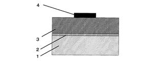
実施例1および2の蛍光体A〜Hの無機蛍光体を用いて直流駆動型無機EL素子を作製した。該直流駆動型無機EL素子の構造の概略を図1に示す。
第1電極2として厚さ200nmのITO層が形成されたガラス基板1に対して、ITO層の上に、実施例1で得られた蛍光体A〜Hをエレクトロンビーム蒸着法により蒸着成膜することで発光層3を形成した。発光層3の膜厚は2μmとし、そのときの蒸着チャンバー内の真空度は1×10⁻⁶Torr、基板1温度は200℃に設定した。さらに、結晶性を向上させるために、成膜した発光層3に対して同一チャンバー内で600℃、1時間熱処理を施した後、発光層3の上に抵抗加熱蒸着法により第2電極4としてAlを蒸着し、発光素子を得た。
得られた発光素子に、Alを正極、ITOを負極として直流電流を流したところ、発光が確認された。
Example 3
Using the inorganic phosphors of the phosphors A to H of Examples 1 and 2, a direct current drive type inorganic EL element was produced. An outline of the structure of the direct current drive type inorganic EL element is shown in FIG.
The phosphors A to H obtained in Example 1 are deposited on the ITO layer by the electron beam evaporation method on the
When a direct current was passed through the obtained light emitting device using Al as a positive electrode and ITO as a negative electrode, light emission was confirmed.
〔実施例4〕
実施例1および2の蛍光体A〜Hの無機蛍光体を用いて直流駆動型無機EL素子を作製した。該直流駆動型無機EL素子の構造の概略を図2に示す。
第1電極2として厚さ200nmのITO層が形成されたガラス基板1に対して、ITO層の上にp型半導体層5としてCu2S層を、さらにその上に、実施例1および2で得られた蛍光体A〜Hをいずれもエレクトロンビーム蒸着法により、同一チャンバー内で連続して蒸着成膜することでp型半導体層5および発光層3を形成した。Cu2S層の膜厚は100nm、発光層3の膜厚は2μmとし、そのときの蒸着チャンバー内の真空度は1×10⁻⁶Torr、基板1温度は200℃に設定した。さらに、結晶性を向上させるために、成膜した発光層3に対して同一チャンバー内で600℃、1時間熱処理を施した後、発光層3の上に抵抗加熱蒸着法により第2電極4としてAlを蒸着し、発光素子を得た。
得られた発光素子に、Alを正極、ITOを負極として直流電流を流したところ、それぞれ実施例3に対して2〜10倍の強度の発光が確認された。
Example 4
Using the inorganic phosphors of the phosphors A to H of Examples 1 and 2, a direct current drive type inorganic EL element was produced. An outline of the structure of the direct current drive type inorganic EL element is shown in FIG.
With respect to the
When a direct current was passed through the obtained light emitting device using Al as a positive electrode and ITO as a negative electrode, light emission of 2 to 10 times the intensity of Example 3 was confirmed.
1 ガラス基板
2 第1電極(ITO電極)
3 発光層
4 第2電極(Al電極)
5 p型半導体層
1
3 Light emitting layer 4 Second electrode (Al electrode)
5 p-type semiconductor layer
Claims (8)
Priority Applications (1)
| Application Number | Priority Date | Filing Date | Title |
|---|---|---|---|
| JP2008154236A JP2009298902A (en) | 2008-06-12 | 2008-06-12 | Inorganic phosphor |
Applications Claiming Priority (1)
| Application Number | Priority Date | Filing Date | Title |
|---|---|---|---|
| JP2008154236A JP2009298902A (en) | 2008-06-12 | 2008-06-12 | Inorganic phosphor |
Publications (2)
| Publication Number | Publication Date |
|---|---|
| JP2009298902A true JP2009298902A (en) | 2009-12-24 |
| JP2009298902A5 JP2009298902A5 (en) | 2011-07-14 |
Family
ID=41546131
Family Applications (1)
| Application Number | Title | Priority Date | Filing Date |
|---|---|---|---|
| JP2008154236A Withdrawn JP2009298902A (en) | 2008-06-12 | 2008-06-12 | Inorganic phosphor |
Country Status (1)
| Country | Link |
|---|---|
| JP (1) | JP2009298902A (en) |
Cited By (1)
| Publication number | Priority date | Publication date | Assignee | Title |
|---|---|---|---|---|
| US9261730B2 (en) | 2013-01-03 | 2016-02-16 | Empire Technology Development Llc | Display devices including inorganic components and methods of making and using the same |
-
2008
- 2008-06-12 JP JP2008154236A patent/JP2009298902A/en not_active Withdrawn
Cited By (1)
| Publication number | Priority date | Publication date | Assignee | Title |
|---|---|---|---|---|
| US9261730B2 (en) | 2013-01-03 | 2016-02-16 | Empire Technology Development Llc | Display devices including inorganic components and methods of making and using the same |
Similar Documents
| Publication | Publication Date | Title |
|---|---|---|
| JP5036710B2 (en) | Luminous body | |
| JP2009167351A (en) | Inorganic phosphor | |
| CN114122272A (en) | Composite material and electroluminescent device | |
| JP2009298902A (en) | Inorganic phosphor | |
| JP2010037370A (en) | Inorganic phosphor particle | |
| JPWO2009072278A1 (en) | Light emitting element | |
| JP2009170358A (en) | Inorganic EL element | |
| JP2010040217A (en) | Inorganic electroluminescent device | |
| JP2010215787A (en) | Inorganic phosphor particle and distributed electroluminescence element using the same | |
| JP2009215450A (en) | Inorganic phosphor | |
| JP2010050421A (en) | Semiconductor | |
| JP5192854B2 (en) | Phosphor and display panel using the same | |
| JP2010031154A (en) | Inorganic phosphor | |
| JP2010061855A (en) | Inorganic EL element | |
| JP5859005B2 (en) | Dispersion type EL device manufacturing method | |
| JP5130996B2 (en) | Light emitting element | |
| JP5046637B2 (en) | Inorganic electroluminescent device | |
| JP2010229178A (en) | Inorganic phosphor material and dispersive electroluminescence device | |
| JP2010218891A (en) | Distributed electroluminescent element | |
| JP5446111B2 (en) | Light emitting device and phosphor material | |
| JPH04100889A (en) | Thin film of luminescent material, preparation thereof, and thin-film electroluminescent element | |
| KR20200142390A (en) | Inorganic electroluminescent device comprising luminescent particle surrounded by a coating layer and method for producing same | |
| JP2009187770A (en) | Light emitting element | |
| JP2010163581A (en) | Inorganic phosphor | |
| JP2010171319A (en) | Light emitting element |
Legal Events
| Date | Code | Title | Description |
|---|---|---|---|
| A521 | Request for written amendment filed |
Free format text: JAPANESE INTERMEDIATE CODE: A523 Effective date: 20110531 |
|
| A621 | Written request for application examination |
Free format text: JAPANESE INTERMEDIATE CODE: A621 Effective date: 20110531 |
|
| A761 | Written withdrawal of application |
Free format text: JAPANESE INTERMEDIATE CODE: A761 Effective date: 20111219 |