JP2009503902A - Metal gate MOSFET obtained by complete conversion to semiconductor metal alloy and method of manufacturing the same - Google Patents
Metal gate MOSFET obtained by complete conversion to semiconductor metal alloy and method of manufacturing the same Download PDFInfo
- Publication number
- JP2009503902A JP2009503902A JP2008525091A JP2008525091A JP2009503902A JP 2009503902 A JP2009503902 A JP 2009503902A JP 2008525091 A JP2008525091 A JP 2008525091A JP 2008525091 A JP2008525091 A JP 2008525091A JP 2009503902 A JP2009503902 A JP 2009503902A
- Authority
- JP
- Japan
- Prior art keywords
- semiconductor
- type mosfet
- metal
- gate
- layer
- Prior art date
- Legal status (The legal status is an assumption and is not a legal conclusion. Google has not performed a legal analysis and makes no representation as to the accuracy of the status listed.)
- Pending
Links
Images


Classifications
-
- H—ELECTRICITY
- H10—SEMICONDUCTOR DEVICES; ELECTRIC SOLID-STATE DEVICES NOT OTHERWISE PROVIDED FOR
- H10P—GENERIC PROCESSES OR APPARATUS FOR THE MANUFACTURE OR TREATMENT OF DEVICES COVERED BY CLASS H10
- H10P10/00—Bonding of wafers, substrates or parts of devices
-
- H—ELECTRICITY
- H10—SEMICONDUCTOR DEVICES; ELECTRIC SOLID-STATE DEVICES NOT OTHERWISE PROVIDED FOR
- H10D—INORGANIC ELECTRIC SEMICONDUCTOR DEVICES
- H10D30/00—Field-effect transistors [FET]
- H10D30/60—Insulated-gate field-effect transistors [IGFET]
- H10D30/601—Insulated-gate field-effect transistors [IGFET] having lightly-doped drain or source extensions, e.g. LDD IGFETs or DDD IGFETs
-
- H—ELECTRICITY
- H10—SEMICONDUCTOR DEVICES; ELECTRIC SOLID-STATE DEVICES NOT OTHERWISE PROVIDED FOR
- H10D—INORGANIC ELECTRIC SEMICONDUCTOR DEVICES
- H10D64/00—Electrodes of devices having potential barriers
- H10D64/01—Manufacture or treatment
- H10D64/017—Manufacture or treatment using dummy gates in processes wherein at least parts of the final gates are self-aligned to the dummy gates, i.e. replacement gate processes
-
- H—ELECTRICITY
- H10—SEMICONDUCTOR DEVICES; ELECTRIC SOLID-STATE DEVICES NOT OTHERWISE PROVIDED FOR
- H10D—INORGANIC ELECTRIC SEMICONDUCTOR DEVICES
- H10D84/00—Integrated devices formed in or on semiconductor substrates that comprise only semiconducting layers, e.g. on Si wafers or on GaAs-on-Si wafers
- H10D84/01—Manufacture or treatment
- H10D84/0123—Integrating together multiple components covered by H10D12/00 or H10D30/00, e.g. integrating multiple IGBTs
- H10D84/0126—Integrating together multiple components covered by H10D12/00 or H10D30/00, e.g. integrating multiple IGBTs the components including insulated gates, e.g. IGFETs
- H10D84/0165—Integrating together multiple components covered by H10D12/00 or H10D30/00, e.g. integrating multiple IGBTs the components including insulated gates, e.g. IGFETs the components including complementary IGFETs, e.g. CMOS devices
-
- H—ELECTRICITY
- H10—SEMICONDUCTOR DEVICES; ELECTRIC SOLID-STATE DEVICES NOT OTHERWISE PROVIDED FOR
- H10D—INORGANIC ELECTRIC SEMICONDUCTOR DEVICES
- H10D84/00—Integrated devices formed in or on semiconductor substrates that comprise only semiconducting layers, e.g. on Si wafers or on GaAs-on-Si wafers
- H10D84/01—Manufacture or treatment
- H10D84/0123—Integrating together multiple components covered by H10D12/00 or H10D30/00, e.g. integrating multiple IGBTs
- H10D84/0126—Integrating together multiple components covered by H10D12/00 or H10D30/00, e.g. integrating multiple IGBTs the components including insulated gates, e.g. IGFETs
- H10D84/0165—Integrating together multiple components covered by H10D12/00 or H10D30/00, e.g. integrating multiple IGBTs the components including insulated gates, e.g. IGFETs the components including complementary IGFETs, e.g. CMOS devices
- H10D84/0172—Manufacturing their gate conductors
- H10D84/0174—Manufacturing their gate conductors the gate conductors being silicided
-
- H—ELECTRICITY
- H10—SEMICONDUCTOR DEVICES; ELECTRIC SOLID-STATE DEVICES NOT OTHERWISE PROVIDED FOR
- H10D—INORGANIC ELECTRIC SEMICONDUCTOR DEVICES
- H10D84/00—Integrated devices formed in or on semiconductor substrates that comprise only semiconducting layers, e.g. on Si wafers or on GaAs-on-Si wafers
- H10D84/01—Manufacture or treatment
- H10D84/0123—Integrating together multiple components covered by H10D12/00 or H10D30/00, e.g. integrating multiple IGBTs
- H10D84/0126—Integrating together multiple components covered by H10D12/00 or H10D30/00, e.g. integrating multiple IGBTs the components including insulated gates, e.g. IGFETs
- H10D84/0165—Integrating together multiple components covered by H10D12/00 or H10D30/00, e.g. integrating multiple IGBTs the components including insulated gates, e.g. IGFETs the components including complementary IGFETs, e.g. CMOS devices
- H10D84/0172—Manufacturing their gate conductors
- H10D84/0177—Manufacturing their gate conductors the gate conductors having different materials or different implants
-
- H—ELECTRICITY
- H10—SEMICONDUCTOR DEVICES; ELECTRIC SOLID-STATE DEVICES NOT OTHERWISE PROVIDED FOR
- H10D—INORGANIC ELECTRIC SEMICONDUCTOR DEVICES
- H10D84/00—Integrated devices formed in or on semiconductor substrates that comprise only semiconducting layers, e.g. on Si wafers or on GaAs-on-Si wafers
- H10D84/01—Manufacture or treatment
- H10D84/02—Manufacture or treatment characterised by using material-based technologies
- H10D84/03—Manufacture or treatment characterised by using material-based technologies using Group IV technology, e.g. silicon technology or silicon-carbide [SiC] technology
- H10D84/038—Manufacture or treatment characterised by using material-based technologies using Group IV technology, e.g. silicon technology or silicon-carbide [SiC] technology using silicon technology, e.g. SiGe
-
- H—ELECTRICITY
- H10—SEMICONDUCTOR DEVICES; ELECTRIC SOLID-STATE DEVICES NOT OTHERWISE PROVIDED FOR
- H10D—INORGANIC ELECTRIC SEMICONDUCTOR DEVICES
- H10D99/00—Subject matter not provided for in other groups of this subclass
-
- H—ELECTRICITY
- H10—SEMICONDUCTOR DEVICES; ELECTRIC SOLID-STATE DEVICES NOT OTHERWISE PROVIDED FOR
- H10D—INORGANIC ELECTRIC SEMICONDUCTOR DEVICES
- H10D30/00—Field-effect transistors [FET]
- H10D30/01—Manufacture or treatment
- H10D30/021—Manufacture or treatment of FETs having insulated gates [IGFET]
- H10D30/0223—Manufacture or treatment of FETs having insulated gates [IGFET] having source and drain regions or source and drain extensions self-aligned to sides of the gate
- H10D30/0227—Manufacture or treatment of FETs having insulated gates [IGFET] having source and drain regions or source and drain extensions self-aligned to sides of the gate having both lightly-doped source and drain extensions and source and drain regions self-aligned to the sides of the gate, e.g. lightly-doped drain [LDD] MOSFET or double-diffused drain [DDD] MOSFET
Landscapes
- Electrodes Of Semiconductors (AREA)
- Metal-Oxide And Bipolar Metal-Oxide Semiconductor Integrated Circuits (AREA)
- Insulated Gate Type Field-Effect Transistor (AREA)
- Thin Film Transistor (AREA)
Abstract
【課題】 MOSFET構造及びその製造方法を提供する。
【解決手段】 本方法は、第一MOSFET型領域(40)では半導体層(22)を完全に半導体金属合金に変換するのに十分な厚さで、第二MOSFET型領域(30)では半導体層(20)を部分的に半導体金属合金に変換するのに十分な厚さで金属含有層(56)を形成する。第一の実施態様では、第一MOSFET型領域(40)のゲートスタックは金属含有層(56)を形成する前に凹化しておくので第一MOSFET半導体スタックの高さは第二MOSFET半導体スタックの高さ未満である。もう一つの実施態様では、変換プロセスの前に第一MOSFET領域(40)よりも第二MOSFET領域(30)の金属含有層(56)を薄く形成する。
【選択図】 図15PROBLEM TO BE SOLVED: To provide a MOSFET structure and a manufacturing method thereof.
The method has a thickness sufficient to completely convert a semiconductor layer (22) into a semiconductor metal alloy in a first MOSFET type region (40), and a semiconductor layer in a second MOSFET type region (30). A metal-containing layer (56) is formed with a thickness sufficient to partially convert (20) to a semiconductor metal alloy. In the first embodiment, the gate stack of the first MOSFET type region (40) is recessed before forming the metal-containing layer (56) so that the height of the first MOSFET semiconductor stack is that of the second MOSFET semiconductor stack. It is less than the height. In another embodiment, the metal-containing layer (56) of the second MOSFET region (30) is formed thinner than the first MOSFET region (40) prior to the conversion process.
[Selection] FIG.
Description
本発明は一般的には集積回路の製造に関し、特に金属ゲートを有するMOSFET素子の構造及び製造方法に関する。 The present invention relates generally to the manufacture of integrated circuits, and more particularly to the structure and method of manufacturing a MOSFET device having a metal gate.
金属ゲート技術によりゲートの空乏層がなくなることによって、半導体MOSFET素子の性能は半導体ゲート電極を用いた従来の半導体MOSFET素子の性能より向上したので、ゲート酸化物リーク電流のさしたる増加を引き起こさずに電気的反転による酸化物の膜厚tinvを約3〜5Å減らすことが可能である。通常、半導体ゲート電極はポリシリコン(ポリ又はポリSi、非晶質Si、SiGe等)から形成される。完全シリサイド化ゲート電極(FUSIゲート)を有するMOSFET素子は電気的反転由来の酸化膜厚を薄くすることを可能にし、その結果チャネルのキャリア密度が増加して素子性能が向上し短チャネル効果の制御性が向上した。ドーパント原子を誘電体境界面へ導入するためにシリサイド化反応の前に行われるポリシリコンゲート電極のプレドーピング及び高温アニールが、それにより形成される金属電極の仕事関数を調整することが最近明らかになってきた。その結果、チャネル注入の補償による閾値電圧の削減の必要がなくなり表面チャネルMOSFETの操作が可能となった。具体的には、n型ドーパントとして周知のアンチモン(Sb)を用いて、標準のポリシリコンゲートプレドーピングステップと同様に約4×1015cm-3に達する高ドープ量でプレドーピングし、次に高温で適切にアニールを行ない、最後にNiを出発材料として完全シリサイド化することによって得られたポリシリコンゲートの仕事関数は、未ドープのNiSiゲートと比較した場合、中間ギャップから、伝導帯端から約120meVのところに移動する。一方、p型ドーパントは仕事関数を価電子帯側に著しく移動可能であることが確認されておらず、完全シリサイド化ゲートをプレドーピングする技術はpFET素子に対して効果が低い。現在用いられている方法で価電子帯端から200meV以内の仕事関数を得ようとすれば、異なった金属シリサイド材料例えばPt濃度が30%のNiPt合金が必要であろう。nFETゲート導電体及びpFETゲート導電体のシリサイド化のためにそれぞれ異なった方法を用いると、特に高密度実装メモリセルにおいてnFET素子及びpFET素子を同時に集積することが困難になる。これ以降、便宜上シリサイド化という語は、半導体金属合金を形成するいかなる方法をも含むものとし、シリサイドという語はその結果得られるあらゆる半導体金属合金を含むものとし、シリサイド化されたという語は半導体金属合金に変換されたあらゆる適切な半導体を含むものとする。これらの使用はシリコン半導体のみを含む方法又は物質に限られない。 By eliminating the gate depletion layer due to the metal gate technology, the performance of the semiconductor MOSFET device is improved from that of the conventional semiconductor MOSFET device using the semiconductor gate electrode, so that the gate oxide leakage current does not increase significantly. It is possible to reduce the oxide film thickness t inv due to mechanical reversal by about 3-5 mm. Usually, the semiconductor gate electrode is made of polysilicon (poly or poly-Si, amorphous Si, SiGe, etc.). A MOSFET device having a fully-silicided gate electrode (FUSI gate) makes it possible to reduce the thickness of the oxide film derived from electrical inversion. As a result, the carrier density of the channel is increased, the device performance is improved, and the short channel effect is controlled. Improved. It has recently become apparent that pre-doping and high temperature annealing of the polysilicon gate electrode prior to the silicidation reaction to introduce dopant atoms into the dielectric interface adjusts the work function of the metal electrode formed thereby. It has become. As a result, it is not necessary to reduce the threshold voltage by compensating for channel injection, and the surface channel MOSFET can be operated. Specifically, using a well-known antimony (Sb) as an n-type dopant, pre-doping with a high doping amount reaching about 4 × 10 15 cm −3 , similar to a standard polysilicon gate pre-doping step, and then The work function of the polysilicon gate obtained by annealing at high temperature and finally fully siliciding with Ni as the starting material is from the intermediate gap, from the conduction band edge, when compared to the undoped NiSi gate. Move to about 120 meV. On the other hand, it has not been confirmed that p-type dopants can remarkably move the work function to the valence band side, and the technique of pre-doping a fully silicided gate is less effective for pFET devices. In order to obtain a work function within 200 meV from the valence band edge by a currently used method, a different metal silicide material, for example, a NiPt alloy having a Pt concentration of 30% will be required. If different methods are used for silicidation of the nFET gate conductor and the pFET gate conductor, it becomes difficult to simultaneously integrate the nFET element and the pFET element, particularly in a high-density mounting memory cell. Hereinafter, for convenience, the term silicidation will include any method of forming a semiconductor metal alloy, the term silicide will include any resulting semiconductor metal alloy, and the term silicidized will refer to a semiconductor metal alloy. Any suitable semiconductor that has been converted shall be included. Their use is not limited to methods or materials that include only silicon semiconductors.
したがって、MOSFETの電気的特性に重大な悪影響を与えずに完全シリサイド化(FUSI)ゲートの向上した性能を利用して、FUSI−MOSFET素子を高密度レイアウトに費用効率よく集積するための構造及び方法を提供することが望ましい。 Accordingly, a structure and method for cost-effectively integrating FUSI-MOSFET devices in a high-density layout utilizing the improved performance of fully silicided (FUSI) gates without significantly adversely affecting the electrical characteristics of the MOSFET. It is desirable to provide
本発明の目的は、半導体ゲートの完全シリサイド化(FUSI)によって得られた金属ゲートの向上した性能をトランジスタの電気的特性を損なうことなく利用する構造及びその構造を製造する方法を提供することである。 It is an object of the present invention to provide a structure that utilizes the improved performance of a metal gate obtained by complete silicidation (FUSI) of a semiconductor gate without damaging the electrical characteristics of the transistor, and a method of manufacturing the structure. is there.
本発明の他の目的は、完全にシリサイド化したnFET又はpFETいずれか一方をnFET又はpFETのもう一方の電気的特性に悪影響を及ぼさずに集積するための費用効率の高い方法を提供することである。 Another object of the present invention is to provide a cost effective method for integrating either fully silicided nFETs or pFETs without adversely affecting the other electrical characteristics of the nFET or pFET. is there.
本発明の更なる目的は、第一タイプの完全シリサイド化FET(例えば、nFET又はpFET)を有する構造を製造し第二タイプの部分的シリサイド化FET構造と共に集積するための費用効率の高い方法を提供することである。例えばnFETが完全シリサイド化ゲートを有する場合、pFETは部分的シリサイド化ゲート有するように製造されてもよい。また、必要に応じてこの逆でもよい。 It is a further object of the present invention to provide a cost effective method for fabricating and integrating a structure having a first type of fully silicided FET (eg, nFET or pFET) with a second type of partially silicided FET structure. Is to provide. For example, if the nFET has a fully silicided gate, the pFET may be fabricated with a partially silicided gate. Moreover, the reverse may be used if necessary.
本発明の更なる目的は、完全シリサイド化(FUSI)nFET素子を提供し、このFUSI−nFET素子を製造し部分的シリサイド化ゲート電極を有するpFET素子と共に集積し、それによりnFET素子及びpFET素子双方とも標準ゲート電極と同程度の閾値電圧を有するようにする方法を提供することである。 It is a further object of the present invention to provide a fully silicided (FUSI) nFET device, which is fabricated and integrated with a pFET device having a partially silicided gate electrode, thereby providing both an nFET device and a pFET device. In other words, a method for providing a threshold voltage comparable to that of the standard gate electrode is provided.
本発明の更なる目的は、nFET素子及びpFET素子の離間距離が約200nm未満である高密度実装回路に集積可能であるFUSI−nFET素子及びpFET素子を提供することである。 It is a further object of the present invention to provide a FUSI-nFET device and a pFET device that can be integrated into a high-density mounting circuit in which the separation distance between the nFET device and the pFET device is less than about 200 nm.
本発明の一態様において提供される半導体構造の製造方法は次のステップを含む。nFET領域のゲートスタックとpFET領域のゲートスタックからなる構造を準備するステップであって、これらゲートスタックはそれぞれ半導体層からなり、この構造はさらにnFET及びpFET領域の前記ゲートスタック上に形成された平坦化誘電体層からなるステップと、平坦化誘電体層の一部を除去してゲートスタックの半導体層を露出するステップと、ゲートスタックの露出した半導体層に接触するように金属含有層を形成するステップであって、この金属含有層は、nFET領域及びpFET領域のうちの第一領域においてはゲートスタックの半導体層を完全にシリサイド化するのに十分な厚さを有するが、nFET領域及びpFET領域のうちの第二領域においては前記半導体層を完全にシリサイド化するのに十分な厚さを有していないステップと、及びnFET領域及びpFET領域のうちの第一領域においてゲートスタックの半導体層に接触する金属含有層から完全シリサイド化ゲート導電体を形成し、nFET領域及びpFET領域のうちの第二領域においてゲートスタックの半導体層に接触する金属含有層から部分シリサイド化ゲート導電体を形成するステップからなる。 A method of manufacturing a semiconductor structure provided in one aspect of the present invention includes the following steps. providing a structure comprising a gate stack of an nFET region and a gate stack of a pFET region, each gate stack comprising a semiconductor layer, the structure further comprising a planar layer formed on the gate stack in the nFET and pFET regions; Forming a dielectric layer, removing a portion of the planarization dielectric layer to expose the semiconductor layer of the gate stack, and forming a metal-containing layer in contact with the exposed semiconductor layer of the gate stack The metal-containing layer has a thickness sufficient to fully silicide the semiconductor layer of the gate stack in the first region of the nFET region and the pFET region, the nFET region and the pFET region The second region of which is thick enough to fully silicide the semiconductor layer Forming a fully silicided gate conductor from a metal-containing layer in contact with the semiconductor layer of the gate stack in a first region of the nFET region and the pFET region; Forming a partially silicided gate conductor from a metal-containing layer in contact with the semiconductor layer of the gate stack in the second region.
本発明の一実施態様によると、金属含有層の形成に先立って、nFET領域及びpFET領域のうちの第一領域のゲートスタックの半導体層を凹化させてその高さをnFET領域及びpFET領域のうちの第二領域のゲートスタックの半導体層の高さ未満にする。好ましくは、nFET領域及びpFET領域のうちの第一領域のゲートスタックの半導体層の凹化は、平坦化誘電体層に対して半導体層を選択的にRIE等で異方エッチングすることにより達成される。 According to an embodiment of the present invention, prior to the formation of the metal-containing layer, the semiconductor layer of the gate stack of the first region of the nFET region and the pFET region is recessed and the height thereof is increased in the nFET region and the pFET region. The height of the semiconductor layer of the gate stack in the second region is less than the height. Preferably, the recessing of the semiconductor layer of the gate stack of the first region of the nFET region and the pFET region is achieved by selectively etching the semiconductor layer with respect to the planarized dielectric layer by RIE or the like. The
本発明の他の実施態様によると、nFET領域及びpFET領域のうちの第一領域上の金属含有層の膜厚と比較して、nFET領域及びpFET領域のうちの第二領域上の金属含有層は薄く形成されている。 According to another embodiment of the present invention, the metal-containing layer on the second region of the nFET region and the pFET region is compared with the film thickness of the metal-containing layer on the first region of the nFET region and the pFET region. Is formed thin.
さらに本発明の他の実施態様により説明されている半導体構造は、半導体層からなる下部ゲート導電体部及び下部ゲート導電体部上の上部シリサイドゲート導電体部を有する部分的シリサイド化ゲート導電体からなるnFET素子及びpFET素子のうちの第一素子、及びnFET素子及びpFET素子のうちの第一素子の部分的シリサイド化ゲート導電体の高さ未満の高さを有する完全シリサイド化ゲート導電体からなるnFET素子及びpFET素子のうちの第二素子からなる。好ましい実施態様においては、本発明の半導体構造は、離間距離が200nm未満であるpFET素子とnFET素子を有する。 In addition, a semiconductor structure described in accordance with another embodiment of the invention comprises a partially silicided gate conductor having a lower gate conductor portion comprising a semiconductor layer and an upper silicide gate conductor portion on the lower gate conductor portion. The first element of the nFET element and the pFET element, and the fully silicided gate conductor having a height less than the height of the partially silicided gate conductor of the first element of the nFET element and the pFET element. It consists of a second element of an nFET element and a pFET element. In a preferred embodiment, the semiconductor structure of the present invention has a pFET element and an nFET element with a separation distance of less than 200 nm.
本発明の更なる態様によると、完全シリサイド化ゲート導電体からなるnPET素子と部分的シリサイド化ゲート導電体からなるpPET素子からなる半導体構造は次のステップを含む方法により製造される。nFET領域のゲートスタックとpFET領域のゲートスタックからなる構造を準備するステップであって、これらゲートスタックはそれぞれ半導体層からなり、上記構造はさらにnFET及びpFET領域のゲートスタック上に形成された平坦化誘電体層からなるステップと、上記平坦化誘電体層の一部を除去してゲートスタックの半導体層を露出するステップと、ゲートスタックの露出した半導体層に接触するように金属含有層を形成するステップで、この金属含有層はnFET領域のゲートスタックの半導体層を完全にシリサイド化するのに十分な厚さを有するが、pFET領域の半導体層を完全にシリサイド化するほど十分な厚さは有していないステップ、及びnFET領域のゲートスタックの半導体層に接触する金属含有層から完全シリサイド化ゲート導電体を形成し、pFET領域のゲートスタックの半導体層に接触する金属含有層から部分シリサイド化ゲート導電体を形成するステップからなる。 According to a further aspect of the present invention, a semiconductor structure comprising an nPET device comprising a fully suicided gate conductor and a pPET device comprising a partially suicided gate conductor is produced by a method comprising the following steps. preparing a structure comprising a gate stack of an nFET region and a gate stack of a pFET region, each gate stack comprising a semiconductor layer, the structure further comprising a planarization formed on the gate stack of the nFET and pFET regions Forming a dielectric layer; removing a portion of the planarizing dielectric layer to expose a semiconductor layer of the gate stack; and forming a metal-containing layer so as to contact the exposed semiconductor layer of the gate stack. In the step, the metal-containing layer has a thickness sufficient to completely silicide the semiconductor layer of the gate stack in the nFET region, but not thick enough to fully silicide the semiconductor layer in the pFET region. And a metal-containing layer in contact with the semiconductor layer of the gate stack in the nFET region. Forming a silicide gate conductor, comprising the step of forming a partially suicided gate conductor from the metal-containing layer in contact with the semiconductor layer of the gate stack of pFET region.
上記及び他の特徴、態様及び効果は、下記の図を参照し、次の本発明の詳細な記載からより容易に明らかになりよりよく理解されるであろう。図において同一の符号は同一の部材を表わし、図はかならずしも一定の縮尺ではない。 These and other features, aspects and advantages will become more readily apparent and better understood from the following detailed description of the invention with reference to the following figures. In the drawings, the same reference numerals represent the same members, and the drawings are not necessarily to scale.
次に、完全シリサイド化ゲート電極を有する第一タイプMOSFET素子(例えば、nFET)と部分的シリサイド化ゲート電極を有する第二タイプ(たとえばpFET)MOSFET素子を共に集積する構造および方法を提供する本発明を、添付された本出願の図を参照してより詳細に説明する。 Next, the present invention provides a structure and method for integrating together a first type MOSFET device (eg, nFET) having a fully silicided gate electrode and a second type (eg, pFET) MOSFET device having a partially silicided gate electrode. Will be described in more detail with reference to the accompanying figures of this application.
本発明に従い提供されたプロセスフローによると、第一タイプMOSFET素子は完全シリサイド化ゲート電極を有し、第二タイプのMOSFET素子は部分的シリサイド化電極を有するので両素子の閾値電圧は標準のポリシリコンゲート電極を用いた場合得られる閾値電圧と同等である。本開示に述べられている技術は、ゲートピッチが約200nm未満の高集積回路に適用可能である。これから述べる例示実施態様において,nFETは完全シリサイド化ゲート電極を有し、pFETは部分的シリサイド化ゲート電極を有するが、本発明はこれら実施態様に限定されることを意図したものではなく、部分的シリサイド化nFETゲート電極と共に集積された完全シリサイド化pFETゲート電極にも同様に適用可能である。ここで述べられている構造は、65nm技術ノードに見合ったおよそ200nmのゲートピッチを有する高密度回路に適用可能であり,これからの技術世代にも応用可能である。 According to the process flow provided in accordance with the present invention, the first type MOSFET device has a fully silicided gate electrode and the second type MOSFET device has a partially silicided electrode so that the threshold voltage of both devices is a standard poly-silicone. This is equivalent to the threshold voltage obtained when a silicon gate electrode is used. The technology described in this disclosure is applicable to highly integrated circuits having a gate pitch of less than about 200 nm. In the exemplary embodiments to be described, nFETs have fully-silicided gate electrodes and pFETs have partially-silicided gate electrodes, but the invention is not intended to be limited to these embodiments, but only partially The same applies to a fully silicided pFET gate electrode integrated with a silicided nFET gate electrode. The structure described here can be applied to high density circuits with a gate pitch of approximately 200 nm commensurate with the 65 nm technology node, and is also applicable to future technology generations.
図1について述べると、図1は初期半導体ウェハ基板10を示し、例えば、限定されないが、バルクシリコン含有基板、シリコン・オン・インシュレーター(SOI)ウェハ等である。シリコン基板又はシリコン含有基板は例えば、限定されないが、Si,SiGe,SiC及びSiGeC半導体などの本発明で用いることができる半導体材料を有することができる。具体的には、図1の初期ウェハ10はnドープウェル領域11とpドープウェル領域12からなる。ゲート誘電体18は基板10上に形成され、基板10には分離領域13が形成されてもよい。分離領域13は、現在周知の或いはこれから開発されるいずれの方法で形成されてもよく、例えば従来のリソグラフィとエッチング方法により溝を形成し、次にこの溝に化学気相成長(CVD)やプラズマCVDなどの方法によりTEOS(テトラエチルオルソシリケート)や酸化物などの誘電体を埋め、次に化学的機械的研磨(CMP)などの平坦化方法を用いて形成してもよい。基板上に従来の熱成長法又は蒸着法によりゲート誘電体18を形成する。ゲート誘電体18は通常、膜厚が約1nmから約10nmの薄層である。このゲート誘電体は例えばSiO2,窒化酸化物,Al2O3,ZrO2,HfO2,Ta2O3,TiO2,ペロブスカイト系酸化物、ケイ酸塩およびこれらの組み合わせに窒素を添加したもの或いは無添加のものなどの酸化物からなるが、これらに限定されるわけではない。このゲート誘電体は熱成長法又は蒸着法を用いて形成してもよい。
Referring to FIG. 1, FIG. 1 shows an initial
この構造の露出表面上にゲート誘電体を形成した後,図2に示したようにnドープウェル領域11及びpドープウェル領域12上にゲートスタック25及び35をそれぞれ形成する。p−FET素子領域30はnドープ領域上に形成されたゲートスタック25からなりn−FET素子領域40はpドープ領域12上に形成されたゲートスタック35からなる。
After forming the gate dielectric on the exposed surface of this structure, gate stacks 25 and 35 are formed on the n-doped
ゲートスタック25、35はそれぞれ1又はまたはそれ以上の半導体層20,22からなり、これらの半導体層は限定されないが、例えばポリシリコン,Ge,SiGe,SiC,SiGeC等の半導体材料を含み、pFET領域30においては例えばp+型ドーパントでドープされた半導体を含んでもよく、nFET領域40においては例えばn+型ドーパントでドープされた半導体を含んでもよい。ゲートスタック25,35はハードマスク層24,26を含んでもよく、これらは一般的にはシリコン窒化物などの窒化物からなる。ゲートスタック25,35は、半導体層及びハードマスク層を堆積し、従来のリソグラフィとエッチング法などのパターン形成方法を用いてウェハ10上に複数のパターン化したスタック領域を形成することによって得られる。
Each of the gate stacks 25, 35 comprises one or more semiconductor layers 20, 22, which include, but are not limited to, semiconductor materials such as, for example, polysilicon, Ge, SiGe, SiC, SiGeC, and
図3について述べると、領域28,29内に示したソース/ドレイン領域を従来のイオン注入を用いてドープ領域11,12内に形成する。例えばn+型ドーパントをpFET領域30のn型ウェル11内のソース/ドレイン領域28に注入し、nFET領域40のp型ウェル12内のソース/ドレイン領域29にp+型ドーパントを注入する。次に、例えば約1000から1100℃の範囲の温度でアニールしてソース/ドレイン領域28,29を活性化する。窒化物や酸窒化物などの絶縁材料を堆積し、次に絶縁材料を選択的にエッチングして、パターン化したスタック領域25,35の露出した垂直側壁面上に絶縁スペーサ27を形成する。スペーサ27は複数のスペーサ及び複数の材料からなってもよく、例えばスペーサ27は窒化物からなる内部スペーサそして酸化物からなる外部スペーサからなってもよい。図3は上記のプロセスステップが終わった後の構造を示したものである。
Referring to FIG. 3, the source / drain regions shown in
図4について述べると、ソース/ドレイン領域28,29上にシリサイド領域32を形成する。好ましい態様においては,自己整合サリサイド法を用いてシリサイド領域32を形成する。好ましい態様においては,例えばスパッタリング、PECVD,電子線蒸着等の適切な方法を用いてニッケル等の金属を蒸着する。この金属としては、シリコンと接触させアニーリングを施した時に金属シリサイドを形成できるいずれの金属を使用してもよい。その中でも、限定するわけではないがCo,Ni,Ti,W,Mo,Ta等が適しており、Ni,Co及びTiが好ましくニッケルが最も好ましい。次に、用いた金属に応じた温度で瞬時熱アニール(RTA)を行なう。例えば金属がNiの場合、好ましくは300〜600℃の温度範囲でRTAを行ないニッケルシリサイド領域32を形成する。次に未反応の金属を除去して図4に示した構造を得る。
Referring to FIG. 4,
次に図5について述べると、シリサイド領域32を含むnFET領域40及びpFET領域30にわたる構造上に薄い誘電体層52を形成する。この薄い誘電体層52は次に行われる反応性イオンエッチング(RIE)法の際にシリサイド領域32を保護するように働く。好ましくは薄い誘電体層52は膜厚約10〜30nmの窒化物である。次に、薄い誘電体層52上に第二誘電体層54を形成する。好ましい態様においては,厚い誘電体層54は酸化物である。厚い誘電体層54はゲートスタック25,35の高さよりも厚く、好ましくはゲートスタックの約1.5から3倍の厚さを有し、より好ましくはゲートスタック25,35の高さの約2から3倍の厚さを有する。ここで得られた構造が図5に示されている。
Referring now to FIG. 5, a
次に、例えば化学的機械的研磨(CMP)により図6のようにウェハを平坦化し、厚い誘電体層54を平坦化するが、平坦化してもなおこの厚い誘電体層はゲートスタック25,35を覆っている。厚い誘電体層54(通常、酸化物)、薄い誘電体層52(通常、窒化物)、ハードマスク24(通常、窒化物)、及びスペーサ27(通常、酸化物と窒化物の組み合わせ)を、例えばRIE71を用いて異方性エッチングし半導体ゲート電極20,22(通常はポリシリコン)を露出する。エッチングステップがポリシリコン上で停止する限り、酸化物と窒化物のエッチ率は一般的には異なるので何らかのトポロジーが存在しうる。その結果図7に示した構造が得られる。
Next, the wafer is planarized as shown in FIG. 6 by chemical mechanical polishing (CMP), for example, and the
図8について述べると、次にその技術における既存のリソグラフィレチクルを用いてフォトレジスト層60でpFET領域30をブロックする。なお本発明においてこのプロセスステップに新しいレチクルを導入する必要はない。次に、誘電体層54,52及びスペーサ27(通常、窒化物及び酸化物)に対して、選択的な異方性ドライドライエッチング、例えばRIEを行ない、nFET半導体ゲート22(通常は、ポリシリコン)を薄くする。nFET半導体ゲート電極22を好ましくは初期膜厚の約2分の1から約3分の1に薄くする。その結果得られたnFETゲート電極は、好ましくは、nFETゲート電極22の完全シリサイド化を可能にするほど十分に薄くなるがpFETゲート電極20についてはこの限りではない。RIEは好ましくは、得られる構造が横に沿ってダメージをうけないように行なうのが好ましく、これは高密度実装ゲートラインにとっては重要なことである(<200nmピッチ)。
Referring to FIG. 8, the
図9について述べると、次にフォトレジストを例えばウエットエッチングによって除去し、それから金属含有層56を堆積して半導体ゲート電極20,22の露出した表面に接触させ、次にゲート電極20,22と反応させる。金属含有層56の組成はnFET30領域及びpFET40領域両方にわたってほぼ一定しているのが好ましい。金属含有層56は、半導体に接触した時に半導体金属合金を形成することが出来るいかなる金属を含んでもよい。半導体材料がシリコンである場合、この半導体金属合金を形成する反応を通常シリサイド化と呼ぶ。以後、シリサイド化という語はSi,Ge,SiGe,SiC,SiGeC,GaAs等の半導体材料とCo,Ni,Ti,W,Mo,Ta等の金属の反応により半導体金属合金を形成するプロセスに言及する場合に用いられる。ただし半導体材料および金属はこれらに限定されない。好ましくは、得られる半導体金属合金(以降、便宜上“シリサイド”と称する)が高濃度ドープポリシリコン等の高濃度にドープされた半導体の仕事関数と同等の仕事関数を有するようにその金属を選択する。ポリシリコンゲート電極にはNi,Co,Tiなどの金属が好ましく、ニッケルが最も好ましい。金属含有層56は、残りのnFETゲート電極22を完全にシリサイド化するのに十分であるがpFETゲート電極20は完全にシリサイド化しない厚さで堆積する。
Referring to FIG. 9, the photoresist is then removed, for example, by wet etching, and then a metal-containing
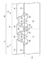
次に、得られた構造を瞬時熱アニール(RTA)に付して金属層56とゲート電極20,22を反応させる。RTAは半導体材料及び金属に応じた温度で行われる。ポリシリコンゲート電極とニッケルの反応の場合300から600℃の温度範囲が好ましく、Coの場合、好ましい温度範囲は550から750℃である。この実施態様において、pFETポリシリコン20はnFETポリシリコン22より厚いので、サリサイド法によりpFET電極20は部分的に消費され一方nFET電極22は完全に消費されて、図10に示すように完全シリサイド化nFETゲート電極62が形成される。pFETゲートスタックは部分的にシリサイド化される。つまりシリサイド部分64と未反応部分20を有する。図15に示すように、得られた構造上に、通常約400から500nmの膜厚を有する層間誘電体(ILD)層70を形成し、nFET素子及びpFET素子を通常通り完成する。
Next, the obtained structure is subjected to instantaneous thermal annealing (RTA) to react the
もう一つの実施態様においては、完全シリサイド化nFETゲートと部分的シリサイド化pFETゲートをドライエッチングではなくウエットエッチングを用いて得る。具体的に図11について述べると、上述の実施態様の図7のステップのすぐ後に、半導体(例えばポリシリコン)ゲート20、22を完全シリサイド化するのに十分な厚さの金属含有層56、好ましくはNiを含有する金属含有層をここに堆積する。次に,図12で示したように、この技術で既存のリソグラフィレチクルを用いてnFET領域40をフォトレジスト層63でブロックする。なお本発明ではプロセスステップに新しいレチクルを導入する必要がない。次に、図13に示すようにp−FET領域から金属を除去するための希薄ウエットエッチに暴露して金属含有層56の膜厚を減らし、次の熱反応において最終的に得られるゲートが完全にシリサイド化されないようにする。なおウエットエッチングは等方的に起こるので横方向にエッチングが起こる。次にウエットエッチングでフォトレジストを除去し、nFET領域40に金属含有層56を残すが、pFET領域30上の金属含有層は薄くなっている。
In another embodiment, fully silicided nFET gates and partially silicided pFET gates are obtained using wet etching rather than dry etching. Specifically referring to FIG. 11, immediately after the step of FIG. 7 of the above-described embodiment, a metal-containing
図14について述べると、得られた構造を瞬時熱アニール(RTA)に付して金属層56とゲート電極20,22を反応させる。反応によってその温度は異なり、例えばポリシリコンゲート電極とNiの場合、RTAは好ましくは300から600℃の温度範囲で行われる。金属がCoである場合、好ましいRTA温度は550から750℃の範囲である。金属含有層56の厚さがpFET領域30上よりもnFET領域40上でのほうが厚いので、得られるnFETゲート35は金属変換領域66を有して完全にシリサイド化され、一方pFETゲート25はポリシリコン20導電体上に形成された金属変換領域65を有して部分的にシリサイド化されている。
Referring to FIG. 14, the obtained structure is subjected to instantaneous thermal annealing (RTA) to react the
最後に、図15で示すように、膜厚が通常約400から500nmの範囲の層間誘電体(ILD)層70を得られた構造上に形成する。次に、nFET素子35及びpFET25素子を通常通りに完成させる。
Finally, as shown in FIG. 15, an interlayer dielectric (ILD)
本発明によると、この方法はnFETの完全シリサイド化及びpFETの部分シリサイド化に限らず、完全シリサイド化pFET及び部分的シリサイド化nFETの形成にも適用可能であり、適宜変更可能である。 According to the present invention, this method is applicable not only to complete silicidation of nFETs and partial silicidation of pFETs, but also to formation of fully silicidized pFETs and partially silicidized nFETs, and can be modified as appropriate.
本発明は、nFETとpFETの一方に金属ゲート技術を用い、nFETとpFETのもう一方に従来のポリシリコンゲート電極技術を適用して高性能CMOS構造を可能にした。完全シリサイド化nFET及び部分シリサイド化pFETの場合、さまざまな周知の技術、例えば性能の向上のために応力を用いるなどして、pFET性能をさらに向上させることが可能である。本発明の構造及び方法は特に、nFET素子とpFET素子の離間距離が約200nm未満で、65nm以上の技術にみあう高密度回路に適用可能である。 The present invention enables a high-performance CMOS structure by using metal gate technology for one of nFET and pFET and applying conventional polysilicon gate electrode technology for the other of nFET and pFET. In the case of fully silicided nFETs and partially silicided pFETs, various well known techniques can be used to further improve pFET performance, such as using stress to improve performance. The structure and method of the present invention is particularly applicable to high density circuits where the separation distance between the nFET and pFET elements is less than about 200 nm and meets technology of 65 nm or more.
本発明をいくつかの好ましい実施態様に従って述べたが、同業者は本発明の真の範囲及び精神から逸脱せずになされうる多くの変更及び改良を理解するであろう。これらは下記の特許請求の範囲によってのみ限定される。 Although the invention has been described in accordance with certain preferred embodiments, those skilled in the art will recognize many variations and modifications that may be made without departing from the true scope and spirit of the invention. These are limited only by the following claims.
本発明による構造及び方法は集積回路の製造に有用であり、nFET及びpFETのうちの一方に金属ゲート技術を用い、もう一方に従来のポリシリコンゲート電極技術を用いた高性能CMOS構造を可能にし、特に、nFETとpFETの距離が200nm未満である65nm以上の技術にみあう高密度回路に適用される。 The structure and method according to the present invention is useful in the manufacture of integrated circuits, enabling high performance CMOS structures using metal gate technology for one of nFETs and pFETs and conventional polysilicon gate electrode technology for the other. In particular, the present invention is applied to a high-density circuit that meets a technology of 65 nm or more in which the distance between nFET and pFET is less than 200 nm.
Claims (20)
前記平坦化誘電体層(54)の一部を除去して前記ゲートスタックの前記半導体層(22,20)を露出するステップと、
前記ゲートスタックの前記露出した半導体層(22,20)に接触するように金属含有層(56)を形成するステップで、前記金属含有層(56)は、前記第一タイプMOSFET領域(40)の前記ゲートスタックの前記半導体層(22)を完全に半導体金属合金に変換する十分な厚さを有しているが、前記第二タイプMOSFET領域(30)の前記半導体層(20)を完全に半導体金属合金に変換する十分な厚さは有していないステップ、及び
前記第一タイプMOSFET領域(40)の前記ゲートスタックの前記半導体層(22)に接触する前記金属含有層(56)から完全変換半導体金属合金ゲート導電体(62,66)を形成し、前記第二タイプMOSFET領域(30)の前記ゲートスタックの前記半導体層(20)に接触する前記金属含有層(56)から部分変換半導体金属合金ゲート導電体を形成するステップを含む半導体構造の製造方法。 In the step of preparing a structure comprising a gate stack of a first type MOSFET region (40) and a gate stack of a second type MOSFET region (30), each of the gate stacks comprises a semiconductor layer (22, 20), and the structure Further comprising a planarizing dielectric layer (54) formed on the gate stack in the first type MOSFET and second type MOSFET regions;
Removing a portion of the planarizing dielectric layer (54) to expose the semiconductor layers (22, 20) of the gate stack;
Forming a metal-containing layer (56) in contact with the exposed semiconductor layer (22, 20) of the gate stack, wherein the metal-containing layer (56) is formed in the first type MOSFET region (40); The semiconductor layer (22) of the gate stack has a sufficient thickness to completely convert to a semiconductor metal alloy, but the semiconductor layer (20) of the second type MOSFET region (30) is completely semiconductor. Full conversion from the metal-containing layer (56) in contact with the semiconductor layer (22) of the gate stack of the first type MOSFET region (40) and not having a sufficient thickness to convert to a metal alloy A semiconductor metal alloy gate conductor (62, 66) is formed and contacts the semiconductor layer (20) of the gate stack of the second type MOSFET region (30). The method of manufacturing a semiconductor structure comprising the steps of forming a partial conversion semiconductor metal alloy gate conductor from said metal-containing layer (56).
半導体層(20)からなる下部ゲート導電体部及び前記下部ゲート導電体部(20)上の上部半導体金属合金ゲート導電体部(64,65)を有する部分変換半導体金属合金ゲート導電体からなる第二タイプMOSFET素子(25)を含む半導体構造であって、前記第一タイプMOSFET素子(35)の前記完全変換半導体金属合金ゲート導電体(62,66)の高さは、前記第二タイプMOSFET素子(25)の前記部分変換半導体金属合金ゲート導電体の高さ未満である半導体構造。 First type MOSFET element (35) made of fully converted semiconductor metal alloy gate conductor, lower gate conductor part made of semiconductor layer (20), and upper semiconductor metal alloy gate conduction on said lower gate conductor part (20) A semiconductor structure comprising a second type MOSFET element (25) comprising a partially converted semiconductor metal alloy gate conductor having a body part (64, 65), wherein the fully converted semiconductor metal of the first type MOSFET element (35) A semiconductor structure in which the height of the alloy gate conductor (62, 66) is less than the height of the partial conversion semiconductor metal alloy gate conductor of the second type MOSFET element (25).
前記平坦化誘電体層(54)の一部を除去して前記ゲートスタックの前記半導体層(22,20)を露出するステップと、
前記ゲートスタックの前記露出した半導体層(22,20)に接触するように金属含有層(56)を形成するステップで、前記金属含有層(56)は、前記第一タイプMOSFET領域(40)の前記ゲートスタックの前記半導体層(22)を完全に半導体金属合金に変換するのに十分な厚さを有するが、前記第二タイプMOSFET領域(30)の前記ゲートスタックの前記半導体層(20)を完全に半導体金属合金に変換するのに十分な厚さは有していないステップ、及び
前記第一タイプMOSFET領域(40)の前記ゲートスタックの前記半導体層(22)に接触する前記金属含有層(56)から完全変換ゲート導電体(62,66)を形成し、前記第二タイプMOSFET領域(30)の前記ゲートスタックの前記半導体層(20)に接触する前記金属含有層(56)から部分変換ゲート導電体を形成するステップを含む方法によって製造される請求項14記載の半導体構造。 In the step of preparing a structure comprising a gate stack of a first type MOSFET region (40) and a gate stack of a second type MOSFET region (30), each of the gate stacks comprises a semiconductor layer (22, 20), Further comprising a planarized dielectric layer (54) formed on the gate stack of the first type MOSFET region and the second type MOSFET region;
Removing a portion of the planarizing dielectric layer (54) to expose the semiconductor layers (22, 20) of the gate stack;
Forming a metal-containing layer (56) in contact with the exposed semiconductor layer (22, 20) of the gate stack, wherein the metal-containing layer (56) is formed in the first type MOSFET region (40); The semiconductor layer (20) of the gate stack of the second type MOSFET region (30) has a thickness sufficient to completely convert the semiconductor layer (22) of the gate stack into a semiconductor metal alloy. A step that does not have a sufficient thickness to completely convert to a semiconductor metal alloy, and the metal-containing layer in contact with the semiconductor layer (22) of the gate stack of the first type MOSFET region (40) 56) to form a complete conversion gate conductor (62, 66) and the semiconductor layer (20) of the gate stack of the second type MOSFET region (30). The semiconductor structure of claim 14 wherein is produced by a method comprising the steps of forming a partial conversion gate conductor from said metal-containing layer in contact (56) on.
Applications Claiming Priority (2)
| Application Number | Priority Date | Filing Date | Title |
|---|---|---|---|
| US11/161,372 US7151023B1 (en) | 2005-08-01 | 2005-08-01 | Metal gate MOSFET by full semiconductor metal alloy conversion |
| PCT/US2006/029800 WO2007016514A2 (en) | 2005-08-01 | 2006-08-01 | Metal gate mosfet by full semiconductor metal alloy conversion |
Publications (2)
| Publication Number | Publication Date |
|---|---|
| JP2009503902A true JP2009503902A (en) | 2009-01-29 |
| JP2009503902A5 JP2009503902A5 (en) | 2009-03-12 |
Family
ID=37526554
Family Applications (1)
| Application Number | Title | Priority Date | Filing Date |
|---|---|---|---|
| JP2008525091A Pending JP2009503902A (en) | 2005-08-01 | 2006-08-01 | Metal gate MOSFET obtained by complete conversion to semiconductor metal alloy and method of manufacturing the same |
Country Status (7)
| Country | Link |
|---|---|
| US (2) | US7151023B1 (en) |
| EP (1) | EP1911088A4 (en) |
| JP (1) | JP2009503902A (en) |
| KR (1) | KR101027107B1 (en) |
| CN (1) | CN101233611A (en) |
| TW (1) | TW200725750A (en) |
| WO (1) | WO2007016514A2 (en) |
Cited By (1)
| Publication number | Priority date | Publication date | Assignee | Title |
|---|---|---|---|---|
| JP2008218544A (en) * | 2007-03-01 | 2008-09-18 | Nec Electronics Corp | Semiconductor device and manufacturing method thereof |
Families Citing this family (41)
| Publication number | Priority date | Publication date | Assignee | Title |
|---|---|---|---|---|
| JP2006344836A (en) * | 2005-06-09 | 2006-12-21 | Matsushita Electric Ind Co Ltd | Semiconductor device and manufacturing method thereof |
| JP2007157744A (en) * | 2005-11-30 | 2007-06-21 | Toshiba Corp | Semiconductor device and manufacturing method of semiconductor device |
| US7732878B2 (en) * | 2006-10-18 | 2010-06-08 | Taiwan Semiconductor Manufacturing Company, Ltd. | MOS devices with continuous contact etch stop layer |
| US7550808B2 (en) * | 2007-01-18 | 2009-06-23 | International Business Machines Corporation | Fully siliciding regions to improve performance |
| US20080206973A1 (en) * | 2007-02-26 | 2008-08-28 | Texas Instrument Inc. | Process method to optimize fully silicided gate (FUSI) thru PAI implant |
| US7737015B2 (en) * | 2007-02-27 | 2010-06-15 | Texas Instruments Incorporated | Formation of fully silicided gate with oxide barrier on the source/drain silicide regions |
| US7768072B2 (en) * | 2007-03-27 | 2010-08-03 | Taiwan Semiconductor Manufacturing Company, Ltd. | Silicided metal gate for multi-threshold voltage configuration |
| US7678694B2 (en) * | 2007-04-18 | 2010-03-16 | Taiwan Semicondutor Manufacturing Company, Ltd. | Method for fabricating semiconductor device with silicided gate |
| US7960243B2 (en) * | 2007-05-31 | 2011-06-14 | Freescale Semiconductor, Inc. | Method of forming a semiconductor device featuring a gate stressor and semiconductor device |
| KR100897818B1 (en) * | 2007-06-08 | 2009-05-15 | 주식회사 동부하이텍 | Pulley silicide silicon gate and method of manufacturing the same |
| US7785952B2 (en) * | 2007-10-16 | 2010-08-31 | International Business Machines Corporation | Partially and fully silicided gate stacks |
| US7749847B2 (en) * | 2008-02-14 | 2010-07-06 | International Business Machines Corporation | CMOS integration scheme employing a silicide electrode and a silicide-germanide alloy electrode |
| US7742324B2 (en) * | 2008-02-19 | 2010-06-22 | Micron Technology, Inc. | Systems and devices including local data lines and methods of using, making, and operating the same |
| US9190494B2 (en) * | 2008-02-19 | 2015-11-17 | Micron Technology, Inc. | Systems and devices including fin field-effect transistors each having U-shaped semiconductor fin |
| US8866254B2 (en) * | 2008-02-19 | 2014-10-21 | Micron Technology, Inc. | Devices including fin transistors robust to gate shorts and methods of making the same |
| US7915659B2 (en) | 2008-03-06 | 2011-03-29 | Micron Technology, Inc. | Devices with cavity-defined gates and methods of making the same |
| US7723192B2 (en) * | 2008-03-14 | 2010-05-25 | Advanced Micro Devices, Inc. | Integrated circuit long and short channel metal gate devices and method of manufacture |
| US7808042B2 (en) * | 2008-03-20 | 2010-10-05 | Micron Technology, Inc. | Systems and devices including multi-gate transistors and methods of using, making, and operating the same |
| US8546876B2 (en) * | 2008-03-20 | 2013-10-01 | Micron Technology, Inc. | Systems and devices including multi-transistor cells and methods of using, making, and operating the same |
| US7898857B2 (en) | 2008-03-20 | 2011-03-01 | Micron Technology, Inc. | Memory structure having volatile and non-volatile memory portions |
| US7969776B2 (en) | 2008-04-03 | 2011-06-28 | Micron Technology, Inc. | Data cells with drivers and methods of making and operating the same |
| US8076229B2 (en) * | 2008-05-30 | 2011-12-13 | Micron Technology, Inc. | Methods of forming data cells and connections to data cells |
| US8237233B2 (en) * | 2008-08-19 | 2012-08-07 | International Business Machines Corporation | Field effect transistor having a gate structure with a first section above a center portion of the channel region and having a first effective work function and second sections above edges of the channel region and having a second effective work function |
| US8148776B2 (en) | 2008-09-15 | 2012-04-03 | Micron Technology, Inc. | Transistor with a passive gate |
| KR20100046888A (en) * | 2008-10-28 | 2010-05-07 | 삼성전자주식회사 | Method of forming gate electrode of semiconductor device |
| US7994038B2 (en) * | 2009-02-05 | 2011-08-09 | Globalfoundries Inc. | Method to reduce MOL damage on NiSi |
| US8680629B2 (en) | 2009-06-03 | 2014-03-25 | International Business Machines Corporation | Control of flatband voltages and threshold voltages in high-k metal gate stacks and structures for CMOS devices |
| US8274116B2 (en) * | 2009-11-16 | 2012-09-25 | International Business Machines Corporation | Control of threshold voltages in high-k metal gate stack and structures for CMOS devices |
| CN102097376B (en) * | 2009-12-10 | 2013-05-01 | 中芯国际集成电路制造(上海)有限公司 | Method for manufacturing semiconductor device |
| US8664070B2 (en) | 2009-12-21 | 2014-03-04 | Taiwan Semiconductor Manufacturing Company, Ltd. | High temperature gate replacement process |
| US8294511B2 (en) | 2010-11-19 | 2012-10-23 | Micron Technology, Inc. | Vertically stacked fin transistors and methods of fabricating and operating the same |
| US8698245B2 (en) | 2010-12-14 | 2014-04-15 | International Business Machines Corporation | Partially depleted (PD) semiconductor-on-insulator (SOI) field effect transistor (FET) structure with a gate-to-body tunnel current region for threshold voltage (VT) lowering and method of forming the structure |
| US8647952B2 (en) | 2010-12-21 | 2014-02-11 | Globalfoundries Inc. | Encapsulation of closely spaced gate electrode structures |
| CN103094086B (en) * | 2011-10-31 | 2016-05-25 | 中芯国际集成电路制造(上海)有限公司 | CMOS formation method |
| US9196704B2 (en) * | 2011-12-19 | 2015-11-24 | Intel Corporation | Selective laser annealing process for buried regions in a MOS device |
| CN103515319B (en) * | 2012-06-20 | 2015-08-19 | 中芯国际集成电路制造(上海)有限公司 | Form the method for CMOS full-silicide metal gate |
| US9524965B2 (en) | 2014-02-12 | 2016-12-20 | Taiwan Semiconductor Manufacturing Co., Ltd. | Gate structures with various widths and method for forming the same |
| US9147683B2 (en) | 2014-02-18 | 2015-09-29 | International Business Machines Corporation | CMOS transistors including gate spacers of the same thickness |
| US9536877B2 (en) * | 2014-03-03 | 2017-01-03 | Globalfoundries Inc. | Methods of forming different spacer structures on integrated circuit products having differing gate pitch dimensions and the resulting products |
| US9484346B2 (en) | 2014-10-15 | 2016-11-01 | Taiwan Semiconductor Manufacturing Company Ltd | Semiconductor structure and manufacturing method thereof |
| DE102020113596A1 (en) * | 2019-07-12 | 2021-01-14 | Taiwan Semiconductor Manufacturing Co., Ltd. | SEMI-CONDUCTOR DEVICE FOR A LOW-LOSS ANTENNA SWITCH |
Citations (10)
| Publication number | Priority date | Publication date | Assignee | Title |
|---|---|---|---|---|
| JPS59125650A (en) * | 1983-01-07 | 1984-07-20 | Toshiba Corp | Semiconductor device and manufacture thereof |
| JPH1174219A (en) * | 1997-06-30 | 1999-03-16 | Toshiba Corp | Semiconductor device manufacturing method and semiconductor device |
| JP2000243853A (en) * | 1999-02-19 | 2000-09-08 | Nec Corp | MIS field-effect transistor and method of manufacturing the same |
| JP2005167251A (en) * | 2003-12-02 | 2005-06-23 | Internatl Business Mach Corp <Ibm> | Manufacturing method of CMOS transistor |
| JP2005228761A (en) * | 2004-02-10 | 2005-08-25 | Rohm Co Ltd | Semiconductor device and its manufacturing method |
| JP2005353655A (en) * | 2004-06-08 | 2005-12-22 | Sanyo Electric Co Ltd | Manufacturing method of semiconductor device |
| JP2006140319A (en) * | 2004-11-12 | 2006-06-01 | Toshiba Corp | Semiconductor device and its fabrication process |
| JP2006278369A (en) * | 2005-03-28 | 2006-10-12 | Fujitsu Ltd | Manufacturing method of semiconductor device |
| JP2006324627A (en) * | 2005-05-16 | 2006-11-30 | Interuniv Micro Electronica Centrum Vzw | Method for forming double fully silicided gates and device obtained by said method |
| JP2008510296A (en) * | 2004-08-13 | 2008-04-03 | コーニンクレッカ フィリップス エレクトロニクス エヌ ヴィ | Manufacturing of dual gate CMOS |
Family Cites Families (16)
| Publication number | Priority date | Publication date | Assignee | Title |
|---|---|---|---|---|
| US6037639A (en) * | 1997-06-09 | 2000-03-14 | Micron Technology, Inc. | Fabrication of integrated devices using nitrogen implantation |
| US6166417A (en) * | 1998-06-30 | 2000-12-26 | Intel Corporation | Complementary metal gates and a process for implementation |
| US20020008257A1 (en) * | 1998-09-30 | 2002-01-24 | John P. Barnak | Mosfet gate electrodes having performance tuned work functions and methods of making same |
| KR100328810B1 (en) * | 1999-07-08 | 2002-03-14 | 윤종용 | Contact structure for a semiconductor device and manufacturing method thereof |
| US6383879B1 (en) * | 1999-12-03 | 2002-05-07 | Agere Systems Guardian Corp. | Semiconductor device having a metal gate with a work function compatible with a semiconductor device |
| US6512269B1 (en) * | 2000-09-07 | 2003-01-28 | International Business Machines Corporation | High-voltage high-speed SOI MOSFET |
| US6562718B1 (en) | 2000-12-06 | 2003-05-13 | Advanced Micro Devices, Inc. | Process for forming fully silicided gates |
| US6846734B2 (en) | 2002-11-20 | 2005-01-25 | International Business Machines Corporation | Method and process to make multiple-threshold metal gates CMOS technology |
| US20050056881A1 (en) * | 2003-09-15 | 2005-03-17 | Yee-Chia Yeo | Dummy pattern for silicide gate electrode |
| US7029966B2 (en) | 2003-09-18 | 2006-04-18 | International Business Machines Corporation | Process options of forming silicided metal gates for advanced CMOS devices |
| US7183182B2 (en) | 2003-09-24 | 2007-02-27 | International Business Machines Corporation | Method and apparatus for fabricating CMOS field effect transistors |
| US7056782B2 (en) * | 2004-02-25 | 2006-06-06 | International Business Machines Corporation | CMOS silicide metal gate integration |
| TWI246116B (en) * | 2004-04-14 | 2005-12-21 | Witty Mate Corp | Process for growing ZnSe Epitaxy layer on Si substrate and semiconductor structure thereby |
| US7105889B2 (en) * | 2004-06-04 | 2006-09-12 | International Business Machines Corporation | Selective implementation of barrier layers to achieve threshold voltage control in CMOS device fabrication with high k dielectrics |
| US7271455B2 (en) * | 2004-07-14 | 2007-09-18 | International Business Machines Corporation | Formation of fully silicided metal gate using dual self-aligned silicide process |
| US7122472B2 (en) * | 2004-12-02 | 2006-10-17 | International Business Machines Corporation | Method for forming self-aligned dual fully silicided gates in CMOS devices |
-
2005
- 2005-08-01 US US11/161,372 patent/US7151023B1/en not_active Expired - Fee Related
-
2006
- 2006-07-28 TW TW095127665A patent/TW200725750A/en unknown
- 2006-08-01 WO PCT/US2006/029800 patent/WO2007016514A2/en not_active Ceased
- 2006-08-01 JP JP2008525091A patent/JP2009503902A/en active Pending
- 2006-08-01 EP EP06789024A patent/EP1911088A4/en not_active Withdrawn
- 2006-08-01 KR KR1020087004254A patent/KR101027107B1/en not_active Expired - Fee Related
- 2006-08-01 CN CNA2006800274429A patent/CN101233611A/en active Pending
- 2006-10-02 US US11/537,718 patent/US20070034967A1/en not_active Abandoned
Patent Citations (10)
| Publication number | Priority date | Publication date | Assignee | Title |
|---|---|---|---|---|
| JPS59125650A (en) * | 1983-01-07 | 1984-07-20 | Toshiba Corp | Semiconductor device and manufacture thereof |
| JPH1174219A (en) * | 1997-06-30 | 1999-03-16 | Toshiba Corp | Semiconductor device manufacturing method and semiconductor device |
| JP2000243853A (en) * | 1999-02-19 | 2000-09-08 | Nec Corp | MIS field-effect transistor and method of manufacturing the same |
| JP2005167251A (en) * | 2003-12-02 | 2005-06-23 | Internatl Business Mach Corp <Ibm> | Manufacturing method of CMOS transistor |
| JP2005228761A (en) * | 2004-02-10 | 2005-08-25 | Rohm Co Ltd | Semiconductor device and its manufacturing method |
| JP2005353655A (en) * | 2004-06-08 | 2005-12-22 | Sanyo Electric Co Ltd | Manufacturing method of semiconductor device |
| JP2008510296A (en) * | 2004-08-13 | 2008-04-03 | コーニンクレッカ フィリップス エレクトロニクス エヌ ヴィ | Manufacturing of dual gate CMOS |
| JP2006140319A (en) * | 2004-11-12 | 2006-06-01 | Toshiba Corp | Semiconductor device and its fabrication process |
| JP2006278369A (en) * | 2005-03-28 | 2006-10-12 | Fujitsu Ltd | Manufacturing method of semiconductor device |
| JP2006324627A (en) * | 2005-05-16 | 2006-11-30 | Interuniv Micro Electronica Centrum Vzw | Method for forming double fully silicided gates and device obtained by said method |
Cited By (1)
| Publication number | Priority date | Publication date | Assignee | Title |
|---|---|---|---|---|
| JP2008218544A (en) * | 2007-03-01 | 2008-09-18 | Nec Electronics Corp | Semiconductor device and manufacturing method thereof |
Also Published As
| Publication number | Publication date |
|---|---|
| KR20080032220A (en) | 2008-04-14 |
| US20070034967A1 (en) | 2007-02-15 |
| TW200725750A (en) | 2007-07-01 |
| EP1911088A4 (en) | 2008-11-12 |
| US7151023B1 (en) | 2006-12-19 |
| WO2007016514A2 (en) | 2007-02-08 |
| KR101027107B1 (en) | 2011-04-05 |
| EP1911088A2 (en) | 2008-04-16 |
| CN101233611A (en) | 2008-07-30 |
| WO2007016514A3 (en) | 2007-04-05 |
Similar Documents
| Publication | Publication Date | Title |
|---|---|---|
| US7151023B1 (en) | Metal gate MOSFET by full semiconductor metal alloy conversion | |
| US8178902B2 (en) | CMOS transistor with dual high-k gate dielectric and method of manufacture thereof | |
| US7964460B2 (en) | Method of manufacturing an NMOS device and a PMOS device | |
| US8012817B2 (en) | Transistor performance improving method with metal gate | |
| US8836038B2 (en) | CMOS dual metal gate semiconductor device | |
| US7229873B2 (en) | Process for manufacturing dual work function metal gates in a microelectronics device | |
| US7294890B2 (en) | Fully salicided (FUSA) MOSFET structure | |
| US20070052037A1 (en) | Semiconductor devices and methods of manufacture thereof | |
| US20100038715A1 (en) | Thin body silicon-on-insulator transistor with borderless self-aligned contacts | |
| CN101221928A (en) | Method for forming double fully silicided gates over fins of field effect transistors | |
| CN101496154A (en) | Fully silicided gate electrodes and method of making the same | |
| JP2012004455A (en) | Method of manufacturing semiconductor device, and semiconductor device | |
| JP2009152342A (en) | Manufacturing method of semiconductor device | |
| JP2012124490A (en) | Semiconductor device and method for manufacturing the same | |
| US20100155844A1 (en) | Semiconductor device and method for manufacturing the same | |
| US20060170047A1 (en) | Semiconductor device and method of manufacturing the same | |
| JP2006054423A (en) | Semiconductor device and manufacturing method thereof | |
| JP3998665B2 (en) | Semiconductor device and manufacturing method thereof | |
| JP4163164B2 (en) | Semiconductor device and manufacturing method thereof | |
| JP2006108355A (en) | Semiconductor device and manufacturing method thereof |
Legal Events
| Date | Code | Title | Description |
|---|---|---|---|
| A521 | Request for written amendment filed |
Free format text: JAPANESE INTERMEDIATE CODE: A523 Effective date: 20090116 |
|
| A621 | Written request for application examination |
Free format text: JAPANESE INTERMEDIATE CODE: A621 Effective date: 20090423 |
|
| A977 | Report on retrieval |
Free format text: JAPANESE INTERMEDIATE CODE: A971007 Effective date: 20110527 |
|
| A131 | Notification of reasons for refusal |
Free format text: JAPANESE INTERMEDIATE CODE: A131 Effective date: 20110607 |
|
| A02 | Decision of refusal |
Free format text: JAPANESE INTERMEDIATE CODE: A02 Effective date: 20111101 |