JP2009503902A - 半導体金属合金への完全変換により得られる金属ゲートmosfet及びその製造方法 - Google Patents
半導体金属合金への完全変換により得られる金属ゲートmosfet及びその製造方法 Download PDFInfo
- Publication number
- JP2009503902A JP2009503902A JP2008525091A JP2008525091A JP2009503902A JP 2009503902 A JP2009503902 A JP 2009503902A JP 2008525091 A JP2008525091 A JP 2008525091A JP 2008525091 A JP2008525091 A JP 2008525091A JP 2009503902 A JP2009503902 A JP 2009503902A
- Authority
- JP
- Japan
- Prior art keywords
- semiconductor
- type mosfet
- metal
- gate
- layer
- Prior art date
- Legal status (The legal status is an assumption and is not a legal conclusion. Google has not performed a legal analysis and makes no representation as to the accuracy of the status listed.)
- Pending
Links
Images


Classifications
-
- H—ELECTRICITY
- H10—SEMICONDUCTOR DEVICES; ELECTRIC SOLID-STATE DEVICES NOT OTHERWISE PROVIDED FOR
- H10P—GENERIC PROCESSES OR APPARATUS FOR THE MANUFACTURE OR TREATMENT OF DEVICES COVERED BY CLASS H10
- H10P10/00—Bonding of wafers, substrates or parts of devices
-
- H—ELECTRICITY
- H10—SEMICONDUCTOR DEVICES; ELECTRIC SOLID-STATE DEVICES NOT OTHERWISE PROVIDED FOR
- H10D—INORGANIC ELECTRIC SEMICONDUCTOR DEVICES
- H10D30/00—Field-effect transistors [FET]
- H10D30/60—Insulated-gate field-effect transistors [IGFET]
- H10D30/601—Insulated-gate field-effect transistors [IGFET] having lightly-doped drain or source extensions, e.g. LDD IGFETs or DDD IGFETs
-
- H—ELECTRICITY
- H10—SEMICONDUCTOR DEVICES; ELECTRIC SOLID-STATE DEVICES NOT OTHERWISE PROVIDED FOR
- H10D—INORGANIC ELECTRIC SEMICONDUCTOR DEVICES
- H10D64/00—Electrodes of devices having potential barriers
- H10D64/01—Manufacture or treatment
- H10D64/017—Manufacture or treatment using dummy gates in processes wherein at least parts of the final gates are self-aligned to the dummy gates, i.e. replacement gate processes
-
- H—ELECTRICITY
- H10—SEMICONDUCTOR DEVICES; ELECTRIC SOLID-STATE DEVICES NOT OTHERWISE PROVIDED FOR
- H10D—INORGANIC ELECTRIC SEMICONDUCTOR DEVICES
- H10D84/00—Integrated devices formed in or on semiconductor substrates that comprise only semiconducting layers, e.g. on Si wafers or on GaAs-on-Si wafers
- H10D84/01—Manufacture or treatment
- H10D84/0123—Integrating together multiple components covered by H10D12/00 or H10D30/00, e.g. integrating multiple IGBTs
- H10D84/0126—Integrating together multiple components covered by H10D12/00 or H10D30/00, e.g. integrating multiple IGBTs the components including insulated gates, e.g. IGFETs
- H10D84/0165—Integrating together multiple components covered by H10D12/00 or H10D30/00, e.g. integrating multiple IGBTs the components including insulated gates, e.g. IGFETs the components including complementary IGFETs, e.g. CMOS devices
-
- H—ELECTRICITY
- H10—SEMICONDUCTOR DEVICES; ELECTRIC SOLID-STATE DEVICES NOT OTHERWISE PROVIDED FOR
- H10D—INORGANIC ELECTRIC SEMICONDUCTOR DEVICES
- H10D84/00—Integrated devices formed in or on semiconductor substrates that comprise only semiconducting layers, e.g. on Si wafers or on GaAs-on-Si wafers
- H10D84/01—Manufacture or treatment
- H10D84/0123—Integrating together multiple components covered by H10D12/00 or H10D30/00, e.g. integrating multiple IGBTs
- H10D84/0126—Integrating together multiple components covered by H10D12/00 or H10D30/00, e.g. integrating multiple IGBTs the components including insulated gates, e.g. IGFETs
- H10D84/0165—Integrating together multiple components covered by H10D12/00 or H10D30/00, e.g. integrating multiple IGBTs the components including insulated gates, e.g. IGFETs the components including complementary IGFETs, e.g. CMOS devices
- H10D84/0172—Manufacturing their gate conductors
- H10D84/0174—Manufacturing their gate conductors the gate conductors being silicided
-
- H—ELECTRICITY
- H10—SEMICONDUCTOR DEVICES; ELECTRIC SOLID-STATE DEVICES NOT OTHERWISE PROVIDED FOR
- H10D—INORGANIC ELECTRIC SEMICONDUCTOR DEVICES
- H10D84/00—Integrated devices formed in or on semiconductor substrates that comprise only semiconducting layers, e.g. on Si wafers or on GaAs-on-Si wafers
- H10D84/01—Manufacture or treatment
- H10D84/0123—Integrating together multiple components covered by H10D12/00 or H10D30/00, e.g. integrating multiple IGBTs
- H10D84/0126—Integrating together multiple components covered by H10D12/00 or H10D30/00, e.g. integrating multiple IGBTs the components including insulated gates, e.g. IGFETs
- H10D84/0165—Integrating together multiple components covered by H10D12/00 or H10D30/00, e.g. integrating multiple IGBTs the components including insulated gates, e.g. IGFETs the components including complementary IGFETs, e.g. CMOS devices
- H10D84/0172—Manufacturing their gate conductors
- H10D84/0177—Manufacturing their gate conductors the gate conductors having different materials or different implants
-
- H—ELECTRICITY
- H10—SEMICONDUCTOR DEVICES; ELECTRIC SOLID-STATE DEVICES NOT OTHERWISE PROVIDED FOR
- H10D—INORGANIC ELECTRIC SEMICONDUCTOR DEVICES
- H10D84/00—Integrated devices formed in or on semiconductor substrates that comprise only semiconducting layers, e.g. on Si wafers or on GaAs-on-Si wafers
- H10D84/01—Manufacture or treatment
- H10D84/02—Manufacture or treatment characterised by using material-based technologies
- H10D84/03—Manufacture or treatment characterised by using material-based technologies using Group IV technology, e.g. silicon technology or silicon-carbide [SiC] technology
- H10D84/038—Manufacture or treatment characterised by using material-based technologies using Group IV technology, e.g. silicon technology or silicon-carbide [SiC] technology using silicon technology, e.g. SiGe
-
- H—ELECTRICITY
- H10—SEMICONDUCTOR DEVICES; ELECTRIC SOLID-STATE DEVICES NOT OTHERWISE PROVIDED FOR
- H10D—INORGANIC ELECTRIC SEMICONDUCTOR DEVICES
- H10D99/00—Subject matter not provided for in other groups of this subclass
-
- H—ELECTRICITY
- H10—SEMICONDUCTOR DEVICES; ELECTRIC SOLID-STATE DEVICES NOT OTHERWISE PROVIDED FOR
- H10D—INORGANIC ELECTRIC SEMICONDUCTOR DEVICES
- H10D30/00—Field-effect transistors [FET]
- H10D30/01—Manufacture or treatment
- H10D30/021—Manufacture or treatment of FETs having insulated gates [IGFET]
- H10D30/0223—Manufacture or treatment of FETs having insulated gates [IGFET] having source and drain regions or source and drain extensions self-aligned to sides of the gate
- H10D30/0227—Manufacture or treatment of FETs having insulated gates [IGFET] having source and drain regions or source and drain extensions self-aligned to sides of the gate having both lightly-doped source and drain extensions and source and drain regions self-aligned to the sides of the gate, e.g. lightly-doped drain [LDD] MOSFET or double-diffused drain [DDD] MOSFET
Landscapes
- Electrodes Of Semiconductors (AREA)
- Metal-Oxide And Bipolar Metal-Oxide Semiconductor Integrated Circuits (AREA)
- Insulated Gate Type Field-Effect Transistor (AREA)
- Thin Film Transistor (AREA)
Abstract
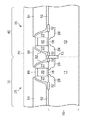
【解決手段】 本方法は、第一MOSFET型領域(40)では半導体層(22)を完全に半導体金属合金に変換するのに十分な厚さで、第二MOSFET型領域(30)では半導体層(20)を部分的に半導体金属合金に変換するのに十分な厚さで金属含有層(56)を形成する。第一の実施態様では、第一MOSFET型領域(40)のゲートスタックは金属含有層(56)を形成する前に凹化しておくので第一MOSFET半導体スタックの高さは第二MOSFET半導体スタックの高さ未満である。もう一つの実施態様では、変換プロセスの前に第一MOSFET領域(40)よりも第二MOSFET領域(30)の金属含有層(56)を薄く形成する。
【選択図】 図15
Description
Claims (20)
- 第一タイプMOSFET領域(40)のゲートスタック及び第二タイプMOSFET領域(30)のゲートスタックからなる構造を準備するステップで、前記のゲートスタックはそれぞれ半導体層(22,20)からなり、前記構造はさらに前記第一タイプMOSFET及び前記第二タイプMOSFET領域の前記ゲートスタック上に形成された平坦化誘電体層(54)からなるステップと、
前記平坦化誘電体層(54)の一部を除去して前記ゲートスタックの前記半導体層(22,20)を露出するステップと、
前記ゲートスタックの前記露出した半導体層(22,20)に接触するように金属含有層(56)を形成するステップで、前記金属含有層(56)は、前記第一タイプMOSFET領域(40)の前記ゲートスタックの前記半導体層(22)を完全に半導体金属合金に変換する十分な厚さを有しているが、前記第二タイプMOSFET領域(30)の前記半導体層(20)を完全に半導体金属合金に変換する十分な厚さは有していないステップ、及び
前記第一タイプMOSFET領域(40)の前記ゲートスタックの前記半導体層(22)に接触する前記金属含有層(56)から完全変換半導体金属合金ゲート導電体(62,66)を形成し、前記第二タイプMOSFET領域(30)の前記ゲートスタックの前記半導体層(20)に接触する前記金属含有層(56)から部分変換半導体金属合金ゲート導電体を形成するステップを含む半導体構造の製造方法。 - 前記ゲートスタックの前記半導体層(22,20)はシリコンからなり、前記金属含有層(56)はシリコンと接触した場合に半導体金属シリサイドを形成しうる金属からなり、高濃度にドープされたポリシリコンとほぼ等しい仕事関数を有する請求項1記載の方法。
- 更に、前記金属含有層(56)を形成する前に,前記第一タイプMOSFET領域(40)の前記ゲートスタックの前記半導体層(22)を凹化し、その高さを前記第二タイプMOSFET領域(30)の前記ゲートスタックの前記半導体層(20)の高さ未満にするステップを含む請求項1記載の方法。
- 前記第一タイプMOSFET領域(40)の前記ゲートスタックの前記半導体層(22)の凹化は、前記平坦化誘電体層(54)に対して前記第一タイプMOSFET領域(40)の前記ゲートスタックの前記半導体層(22)を選択的に異方性エッチングすることからなる請求項3記載の方法。
- 前記金属含有層(56)はニッケルからなり、前記ゲートスタックの前記完全変換半導体金属合金ゲート導電体および前記部分変換半導体金属合金ゲート導電体の形成は300から600℃の温度で瞬時熱アニーリングすることにより行なわれる請求項3記載の方法。
- 前記金属含有層(56)の形成ステップはさらに、前記第二タイプのMOSFET領域(30)上の前記金属含有層(56)を前記第一タイプMOSFET領域(40)上の前記金属含有層(56)の膜厚よりも薄くするステップを含む請求項1記載の方法。
- 前記第二タイプMOSFET領域(30)上の前記金属含有層(56)の薄膜化は、さらに前記第一タイプMOSFET領域(40)上にマスキング層(63)を形成するステップ及び前記第二タイプMOSFET領域(30)上の前記金属含有層(56)をウエットエッチングするステップを含む請求項6記載の方法。
- 前記ウエットエッチングするステップは希薄ウエットエッチングからなる請求項7記載の方法。
- 前記金属含有層(56)はニッケルからなり、前記完全変換半導体金属合金ゲート導電体及び部分変換半導体金属合金ゲート導電体の形成は、300から600℃の温度で瞬時熱アニールすることにより行なわれる請求項6記載の方法。
- 前記金属含有層(56)はニッケルからなり、前記完全変換半導体金属合金ゲート導電体及び部分変換半導体金属合金ゲート導電体の形成は300から600℃の温度で瞬時熱アニールすることにより行なわれる請求項1記載の方法。
- 前記ゲートスタックの前記半導体層(22,20)はSi,Ge,SiGe,SiC,SiGeC及びGaAsからなる群から選択される半導体からなる請求項1記載の方法。
- 前記ゲートスタックの前記半導体層(22,20)はSi,Ge,SiGe,SiC,SiGeC及びGaAsからなる群から選択される半導体からなる請求項3記載の方法。
- 前記ゲートスタックの前記半導体層(22,20)はSi,Ge,SiGe,SiC,SiGeC及びGaAsからなる群から選択される半導体からなる請求項6記載の方法。
- 完全変換半導体金属合金ゲート導電体からなる第一タイプMOSFET素子(35)、及び
半導体層(20)からなる下部ゲート導電体部及び前記下部ゲート導電体部(20)上の上部半導体金属合金ゲート導電体部(64,65)を有する部分変換半導体金属合金ゲート導電体からなる第二タイプMOSFET素子(25)を含む半導体構造であって、前記第一タイプMOSFET素子(35)の前記完全変換半導体金属合金ゲート導電体(62,66)の高さは、前記第二タイプMOSFET素子(25)の前記部分変換半導体金属合金ゲート導電体の高さ未満である半導体構造。 - 前記第一タイプMOSFET素子(35)及び前記第二タイプMOSFET素子(25)の離間距離は200nm未満である請求項14記載の半導体構造。
- 前記第一タイプMOSFET素子(35)の前記完全変換半導体金属合金ゲート導電体及び前記第二タイプMOSFET素子(25)の前記上部半導体金属合金ゲート導電体部(64,65)はニッケルシリサイドを含む請求項14記載の半導体構造。
- 第一タイプMOSFET領域(40)のゲートスタック及び第二タイプMOSFET領域(30)のゲートスタックからなる構造を準備するステップで,前記ゲートスタックはそれぞれ半導体層(22,20)からなり、前記構造はさらに前記第一タイプMOSFET領域及び第二タイプMOSFET領域の前記ゲートスタック上に形成された平坦化誘電体層(54)からなるステップと、
前記平坦化誘電体層(54)の一部を除去して前記ゲートスタックの前記半導体層(22,20)を露出するステップと、
前記ゲートスタックの前記露出した半導体層(22,20)に接触するように金属含有層(56)を形成するステップで、前記金属含有層(56)は、前記第一タイプMOSFET領域(40)の前記ゲートスタックの前記半導体層(22)を完全に半導体金属合金に変換するのに十分な厚さを有するが、前記第二タイプMOSFET領域(30)の前記ゲートスタックの前記半導体層(20)を完全に半導体金属合金に変換するのに十分な厚さは有していないステップ、及び
前記第一タイプMOSFET領域(40)の前記ゲートスタックの前記半導体層(22)に接触する前記金属含有層(56)から完全変換ゲート導電体(62,66)を形成し、前記第二タイプMOSFET領域(30)の前記ゲートスタックの前記半導体層(20)に接触する前記金属含有層(56)から部分変換ゲート導電体を形成するステップを含む方法によって製造される請求項14記載の半導体構造。 - 前記金属含有層(56)を形成する前に,前記第一タイプMOSFET領域(40)の前記ゲートスタックの前記半導体層(22)を凹化して、前記第二タイプMOSFET領域(30)の前記ゲートスタックの前記半導体層(20)の高さ未満にするステップを更に含む前記方法で製造される請求項17記載の半導体構造。
- 前記第一タイプMOSFET領域(40)がnFET領域であり、前記第二タイプのMOSFET領域(30)がpFET領域である請求項1記載の方法。
- 前記第一タイプMOSFET素子(35)がnFET素子で前記第二タイプのMOSFET素子(25)がpFET素子である請求項14記載の方法。
Applications Claiming Priority (2)
| Application Number | Priority Date | Filing Date | Title |
|---|---|---|---|
| US11/161,372 US7151023B1 (en) | 2005-08-01 | 2005-08-01 | Metal gate MOSFET by full semiconductor metal alloy conversion |
| PCT/US2006/029800 WO2007016514A2 (en) | 2005-08-01 | 2006-08-01 | Metal gate mosfet by full semiconductor metal alloy conversion |
Publications (2)
| Publication Number | Publication Date |
|---|---|
| JP2009503902A true JP2009503902A (ja) | 2009-01-29 |
| JP2009503902A5 JP2009503902A5 (ja) | 2009-03-12 |
Family
ID=37526554
Family Applications (1)
| Application Number | Title | Priority Date | Filing Date |
|---|---|---|---|
| JP2008525091A Pending JP2009503902A (ja) | 2005-08-01 | 2006-08-01 | 半導体金属合金への完全変換により得られる金属ゲートmosfet及びその製造方法 |
Country Status (7)
| Country | Link |
|---|---|
| US (2) | US7151023B1 (ja) |
| EP (1) | EP1911088A4 (ja) |
| JP (1) | JP2009503902A (ja) |
| KR (1) | KR101027107B1 (ja) |
| CN (1) | CN101233611A (ja) |
| TW (1) | TW200725750A (ja) |
| WO (1) | WO2007016514A2 (ja) |
Cited By (1)
| Publication number | Priority date | Publication date | Assignee | Title |
|---|---|---|---|---|
| JP2008218544A (ja) * | 2007-03-01 | 2008-09-18 | Nec Electronics Corp | 半導体装置およびその製造方法 |
Families Citing this family (41)
| Publication number | Priority date | Publication date | Assignee | Title |
|---|---|---|---|---|
| JP2006344836A (ja) * | 2005-06-09 | 2006-12-21 | Matsushita Electric Ind Co Ltd | 半導体装置及びその製造方法 |
| JP2007157744A (ja) * | 2005-11-30 | 2007-06-21 | Toshiba Corp | 半導体装置および半導体装置の製造方法 |
| US7732878B2 (en) * | 2006-10-18 | 2010-06-08 | Taiwan Semiconductor Manufacturing Company, Ltd. | MOS devices with continuous contact etch stop layer |
| US7550808B2 (en) * | 2007-01-18 | 2009-06-23 | International Business Machines Corporation | Fully siliciding regions to improve performance |
| US20080206973A1 (en) * | 2007-02-26 | 2008-08-28 | Texas Instrument Inc. | Process method to optimize fully silicided gate (FUSI) thru PAI implant |
| US7737015B2 (en) * | 2007-02-27 | 2010-06-15 | Texas Instruments Incorporated | Formation of fully silicided gate with oxide barrier on the source/drain silicide regions |
| US7768072B2 (en) * | 2007-03-27 | 2010-08-03 | Taiwan Semiconductor Manufacturing Company, Ltd. | Silicided metal gate for multi-threshold voltage configuration |
| US7678694B2 (en) * | 2007-04-18 | 2010-03-16 | Taiwan Semicondutor Manufacturing Company, Ltd. | Method for fabricating semiconductor device with silicided gate |
| US7960243B2 (en) * | 2007-05-31 | 2011-06-14 | Freescale Semiconductor, Inc. | Method of forming a semiconductor device featuring a gate stressor and semiconductor device |
| KR100897818B1 (ko) * | 2007-06-08 | 2009-05-15 | 주식회사 동부하이텍 | 풀리 실리사이드 실리콘 게이트 및 그의 제조방법 |
| US7785952B2 (en) * | 2007-10-16 | 2010-08-31 | International Business Machines Corporation | Partially and fully silicided gate stacks |
| US7749847B2 (en) * | 2008-02-14 | 2010-07-06 | International Business Machines Corporation | CMOS integration scheme employing a silicide electrode and a silicide-germanide alloy electrode |
| US7742324B2 (en) * | 2008-02-19 | 2010-06-22 | Micron Technology, Inc. | Systems and devices including local data lines and methods of using, making, and operating the same |
| US9190494B2 (en) * | 2008-02-19 | 2015-11-17 | Micron Technology, Inc. | Systems and devices including fin field-effect transistors each having U-shaped semiconductor fin |
| US8866254B2 (en) * | 2008-02-19 | 2014-10-21 | Micron Technology, Inc. | Devices including fin transistors robust to gate shorts and methods of making the same |
| US7915659B2 (en) | 2008-03-06 | 2011-03-29 | Micron Technology, Inc. | Devices with cavity-defined gates and methods of making the same |
| US7723192B2 (en) * | 2008-03-14 | 2010-05-25 | Advanced Micro Devices, Inc. | Integrated circuit long and short channel metal gate devices and method of manufacture |
| US7808042B2 (en) * | 2008-03-20 | 2010-10-05 | Micron Technology, Inc. | Systems and devices including multi-gate transistors and methods of using, making, and operating the same |
| US8546876B2 (en) * | 2008-03-20 | 2013-10-01 | Micron Technology, Inc. | Systems and devices including multi-transistor cells and methods of using, making, and operating the same |
| US7898857B2 (en) | 2008-03-20 | 2011-03-01 | Micron Technology, Inc. | Memory structure having volatile and non-volatile memory portions |
| US7969776B2 (en) | 2008-04-03 | 2011-06-28 | Micron Technology, Inc. | Data cells with drivers and methods of making and operating the same |
| US8076229B2 (en) * | 2008-05-30 | 2011-12-13 | Micron Technology, Inc. | Methods of forming data cells and connections to data cells |
| US8237233B2 (en) * | 2008-08-19 | 2012-08-07 | International Business Machines Corporation | Field effect transistor having a gate structure with a first section above a center portion of the channel region and having a first effective work function and second sections above edges of the channel region and having a second effective work function |
| US8148776B2 (en) | 2008-09-15 | 2012-04-03 | Micron Technology, Inc. | Transistor with a passive gate |
| KR20100046888A (ko) * | 2008-10-28 | 2010-05-07 | 삼성전자주식회사 | 반도체 소자의 게이트 전극 형성 방법 |
| US7994038B2 (en) * | 2009-02-05 | 2011-08-09 | Globalfoundries Inc. | Method to reduce MOL damage on NiSi |
| US8680629B2 (en) | 2009-06-03 | 2014-03-25 | International Business Machines Corporation | Control of flatband voltages and threshold voltages in high-k metal gate stacks and structures for CMOS devices |
| US8274116B2 (en) * | 2009-11-16 | 2012-09-25 | International Business Machines Corporation | Control of threshold voltages in high-k metal gate stack and structures for CMOS devices |
| CN102097376B (zh) * | 2009-12-10 | 2013-05-01 | 中芯国际集成电路制造(上海)有限公司 | 半导体器件的制作方法 |
| US8664070B2 (en) | 2009-12-21 | 2014-03-04 | Taiwan Semiconductor Manufacturing Company, Ltd. | High temperature gate replacement process |
| US8294511B2 (en) | 2010-11-19 | 2012-10-23 | Micron Technology, Inc. | Vertically stacked fin transistors and methods of fabricating and operating the same |
| US8698245B2 (en) | 2010-12-14 | 2014-04-15 | International Business Machines Corporation | Partially depleted (PD) semiconductor-on-insulator (SOI) field effect transistor (FET) structure with a gate-to-body tunnel current region for threshold voltage (VT) lowering and method of forming the structure |
| US8647952B2 (en) | 2010-12-21 | 2014-02-11 | Globalfoundries Inc. | Encapsulation of closely spaced gate electrode structures |
| CN103094086B (zh) * | 2011-10-31 | 2016-05-25 | 中芯国际集成电路制造(上海)有限公司 | Cmos形成方法 |
| US9196704B2 (en) * | 2011-12-19 | 2015-11-24 | Intel Corporation | Selective laser annealing process for buried regions in a MOS device |
| CN103515319B (zh) * | 2012-06-20 | 2015-08-19 | 中芯国际集成电路制造(上海)有限公司 | 形成cmos全硅化物金属栅的方法 |
| US9524965B2 (en) | 2014-02-12 | 2016-12-20 | Taiwan Semiconductor Manufacturing Co., Ltd. | Gate structures with various widths and method for forming the same |
| US9147683B2 (en) | 2014-02-18 | 2015-09-29 | International Business Machines Corporation | CMOS transistors including gate spacers of the same thickness |
| US9536877B2 (en) * | 2014-03-03 | 2017-01-03 | Globalfoundries Inc. | Methods of forming different spacer structures on integrated circuit products having differing gate pitch dimensions and the resulting products |
| US9484346B2 (en) | 2014-10-15 | 2016-11-01 | Taiwan Semiconductor Manufacturing Company Ltd | Semiconductor structure and manufacturing method thereof |
| DE102020113596A1 (de) * | 2019-07-12 | 2021-01-14 | Taiwan Semiconductor Manufacturing Co., Ltd. | Halbleitervorrichtung für einen verlustarmen antennenschalter |
Citations (10)
| Publication number | Priority date | Publication date | Assignee | Title |
|---|---|---|---|---|
| JPS59125650A (ja) * | 1983-01-07 | 1984-07-20 | Toshiba Corp | 半導体装置の製造方法 |
| JPH1174219A (ja) * | 1997-06-30 | 1999-03-16 | Toshiba Corp | 半導体装置の製造方法および半導体装置 |
| JP2000243853A (ja) * | 1999-02-19 | 2000-09-08 | Nec Corp | Mis型電界効果トランジスタ及びその製造方法 |
| JP2005167251A (ja) * | 2003-12-02 | 2005-06-23 | Internatl Business Mach Corp <Ibm> | Cmosトランジスタの製造方法 |
| JP2005228761A (ja) * | 2004-02-10 | 2005-08-25 | Rohm Co Ltd | 半導体装置及びその製造方法 |
| JP2005353655A (ja) * | 2004-06-08 | 2005-12-22 | Sanyo Electric Co Ltd | 半導体装置の製造方法 |
| JP2006140319A (ja) * | 2004-11-12 | 2006-06-01 | Toshiba Corp | 半導体装置およびその製造方法 |
| JP2006278369A (ja) * | 2005-03-28 | 2006-10-12 | Fujitsu Ltd | 半導体装置の製造方法 |
| JP2006324627A (ja) * | 2005-05-16 | 2006-11-30 | Interuniv Micro Electronica Centrum Vzw | 二重の完全ケイ化ゲートを形成する方法と前記方法によって得られたデバイス |
| JP2008510296A (ja) * | 2004-08-13 | 2008-04-03 | コーニンクレッカ フィリップス エレクトロニクス エヌ ヴィ | デュアル・ゲートcmosの製造 |
Family Cites Families (16)
| Publication number | Priority date | Publication date | Assignee | Title |
|---|---|---|---|---|
| US6037639A (en) * | 1997-06-09 | 2000-03-14 | Micron Technology, Inc. | Fabrication of integrated devices using nitrogen implantation |
| US6166417A (en) * | 1998-06-30 | 2000-12-26 | Intel Corporation | Complementary metal gates and a process for implementation |
| US20020008257A1 (en) * | 1998-09-30 | 2002-01-24 | John P. Barnak | Mosfet gate electrodes having performance tuned work functions and methods of making same |
| KR100328810B1 (ko) * | 1999-07-08 | 2002-03-14 | 윤종용 | 반도체 장치를 위한 콘택 구조 및 제조 방법 |
| US6383879B1 (en) * | 1999-12-03 | 2002-05-07 | Agere Systems Guardian Corp. | Semiconductor device having a metal gate with a work function compatible with a semiconductor device |
| US6512269B1 (en) * | 2000-09-07 | 2003-01-28 | International Business Machines Corporation | High-voltage high-speed SOI MOSFET |
| US6562718B1 (en) | 2000-12-06 | 2003-05-13 | Advanced Micro Devices, Inc. | Process for forming fully silicided gates |
| US6846734B2 (en) | 2002-11-20 | 2005-01-25 | International Business Machines Corporation | Method and process to make multiple-threshold metal gates CMOS technology |
| US20050056881A1 (en) * | 2003-09-15 | 2005-03-17 | Yee-Chia Yeo | Dummy pattern for silicide gate electrode |
| US7029966B2 (en) | 2003-09-18 | 2006-04-18 | International Business Machines Corporation | Process options of forming silicided metal gates for advanced CMOS devices |
| US7183182B2 (en) | 2003-09-24 | 2007-02-27 | International Business Machines Corporation | Method and apparatus for fabricating CMOS field effect transistors |
| US7056782B2 (en) * | 2004-02-25 | 2006-06-06 | International Business Machines Corporation | CMOS silicide metal gate integration |
| TWI246116B (en) * | 2004-04-14 | 2005-12-21 | Witty Mate Corp | Process for growing ZnSe Epitaxy layer on Si substrate and semiconductor structure thereby |
| US7105889B2 (en) * | 2004-06-04 | 2006-09-12 | International Business Machines Corporation | Selective implementation of barrier layers to achieve threshold voltage control in CMOS device fabrication with high k dielectrics |
| US7271455B2 (en) * | 2004-07-14 | 2007-09-18 | International Business Machines Corporation | Formation of fully silicided metal gate using dual self-aligned silicide process |
| US7122472B2 (en) * | 2004-12-02 | 2006-10-17 | International Business Machines Corporation | Method for forming self-aligned dual fully silicided gates in CMOS devices |
-
2005
- 2005-08-01 US US11/161,372 patent/US7151023B1/en not_active Expired - Fee Related
-
2006
- 2006-07-28 TW TW095127665A patent/TW200725750A/zh unknown
- 2006-08-01 WO PCT/US2006/029800 patent/WO2007016514A2/en not_active Ceased
- 2006-08-01 JP JP2008525091A patent/JP2009503902A/ja active Pending
- 2006-08-01 EP EP06789024A patent/EP1911088A4/en not_active Withdrawn
- 2006-08-01 KR KR1020087004254A patent/KR101027107B1/ko not_active Expired - Fee Related
- 2006-08-01 CN CNA2006800274429A patent/CN101233611A/zh active Pending
- 2006-10-02 US US11/537,718 patent/US20070034967A1/en not_active Abandoned
Patent Citations (10)
| Publication number | Priority date | Publication date | Assignee | Title |
|---|---|---|---|---|
| JPS59125650A (ja) * | 1983-01-07 | 1984-07-20 | Toshiba Corp | 半導体装置の製造方法 |
| JPH1174219A (ja) * | 1997-06-30 | 1999-03-16 | Toshiba Corp | 半導体装置の製造方法および半導体装置 |
| JP2000243853A (ja) * | 1999-02-19 | 2000-09-08 | Nec Corp | Mis型電界効果トランジスタ及びその製造方法 |
| JP2005167251A (ja) * | 2003-12-02 | 2005-06-23 | Internatl Business Mach Corp <Ibm> | Cmosトランジスタの製造方法 |
| JP2005228761A (ja) * | 2004-02-10 | 2005-08-25 | Rohm Co Ltd | 半導体装置及びその製造方法 |
| JP2005353655A (ja) * | 2004-06-08 | 2005-12-22 | Sanyo Electric Co Ltd | 半導体装置の製造方法 |
| JP2008510296A (ja) * | 2004-08-13 | 2008-04-03 | コーニンクレッカ フィリップス エレクトロニクス エヌ ヴィ | デュアル・ゲートcmosの製造 |
| JP2006140319A (ja) * | 2004-11-12 | 2006-06-01 | Toshiba Corp | 半導体装置およびその製造方法 |
| JP2006278369A (ja) * | 2005-03-28 | 2006-10-12 | Fujitsu Ltd | 半導体装置の製造方法 |
| JP2006324627A (ja) * | 2005-05-16 | 2006-11-30 | Interuniv Micro Electronica Centrum Vzw | 二重の完全ケイ化ゲートを形成する方法と前記方法によって得られたデバイス |
Cited By (1)
| Publication number | Priority date | Publication date | Assignee | Title |
|---|---|---|---|---|
| JP2008218544A (ja) * | 2007-03-01 | 2008-09-18 | Nec Electronics Corp | 半導体装置およびその製造方法 |
Also Published As
| Publication number | Publication date |
|---|---|
| KR20080032220A (ko) | 2008-04-14 |
| US20070034967A1 (en) | 2007-02-15 |
| TW200725750A (en) | 2007-07-01 |
| EP1911088A4 (en) | 2008-11-12 |
| US7151023B1 (en) | 2006-12-19 |
| WO2007016514A2 (en) | 2007-02-08 |
| KR101027107B1 (ko) | 2011-04-05 |
| EP1911088A2 (en) | 2008-04-16 |
| CN101233611A (zh) | 2008-07-30 |
| WO2007016514A3 (en) | 2007-04-05 |
Similar Documents
| Publication | Publication Date | Title |
|---|---|---|
| US7151023B1 (en) | Metal gate MOSFET by full semiconductor metal alloy conversion | |
| US8178902B2 (en) | CMOS transistor with dual high-k gate dielectric and method of manufacture thereof | |
| US7964460B2 (en) | Method of manufacturing an NMOS device and a PMOS device | |
| US8012817B2 (en) | Transistor performance improving method with metal gate | |
| US8836038B2 (en) | CMOS dual metal gate semiconductor device | |
| US7229873B2 (en) | Process for manufacturing dual work function metal gates in a microelectronics device | |
| US7294890B2 (en) | Fully salicided (FUSA) MOSFET structure | |
| US20070052037A1 (en) | Semiconductor devices and methods of manufacture thereof | |
| US20100038715A1 (en) | Thin body silicon-on-insulator transistor with borderless self-aligned contacts | |
| CN101221928A (zh) | 用于在场效应晶体管的鳍之上形成双重全硅化栅极的方法 | |
| CN101496154A (zh) | 全硅化栅电极及其制造方法 | |
| JP2012004455A (ja) | 半導体装置の製造方法及び半導体装置 | |
| JP2009152342A (ja) | 半導体装置の製造方法 | |
| JP2012124490A (ja) | 半導体装置及びその製造方法 | |
| US20100155844A1 (en) | Semiconductor device and method for manufacturing the same | |
| US20060170047A1 (en) | Semiconductor device and method of manufacturing the same | |
| JP2006054423A (ja) | 半導体装置及びその製造方法 | |
| JP3998665B2 (ja) | 半導体装置およびその製造方法 | |
| JP4163164B2 (ja) | 半導体装置およびその製造方法 | |
| JP2006108355A (ja) | 半導体装置およびその製造方法 |
Legal Events
| Date | Code | Title | Description |
|---|---|---|---|
| A521 | Request for written amendment filed |
Free format text: JAPANESE INTERMEDIATE CODE: A523 Effective date: 20090116 |
|
| A621 | Written request for application examination |
Free format text: JAPANESE INTERMEDIATE CODE: A621 Effective date: 20090423 |
|
| A977 | Report on retrieval |
Free format text: JAPANESE INTERMEDIATE CODE: A971007 Effective date: 20110527 |
|
| A131 | Notification of reasons for refusal |
Free format text: JAPANESE INTERMEDIATE CODE: A131 Effective date: 20110607 |
|
| A02 | Decision of refusal |
Free format text: JAPANESE INTERMEDIATE CODE: A02 Effective date: 20111101 |