JP2010141089A - Optical receiving module, and method of manufacturing the same - Google Patents
Optical receiving module, and method of manufacturing the same Download PDFInfo
- Publication number
- JP2010141089A JP2010141089A JP2008315422A JP2008315422A JP2010141089A JP 2010141089 A JP2010141089 A JP 2010141089A JP 2008315422 A JP2008315422 A JP 2008315422A JP 2008315422 A JP2008315422 A JP 2008315422A JP 2010141089 A JP2010141089 A JP 2010141089A
- Authority
- JP
- Japan
- Prior art keywords
- light receiving
- receiving element
- light
- optical
- support member
- Prior art date
- Legal status (The legal status is an assumption and is not a legal conclusion. Google has not performed a legal analysis and makes no representation as to the accuracy of the status listed.)
- Granted
Links
Images

Classifications
-
- G—PHYSICS
- G02—OPTICS
- G02B—OPTICAL ELEMENTS, SYSTEMS OR APPARATUS
- G02B6/00—Light guides; Structural details of arrangements comprising light guides and other optical elements, e.g. couplings
- G02B6/24—Coupling light guides
- G02B6/42—Coupling light guides with opto-electronic elements
- G02B6/4201—Packages, e.g. shape, construction, internal or external details
- G02B6/4202—Packages, e.g. shape, construction, internal or external details for coupling an active element with fibres without intermediate optical elements, e.g. fibres with plane ends, fibres with shaped ends, bundles
- G02B6/4203—Optical features
-
- Y—GENERAL TAGGING OF NEW TECHNOLOGICAL DEVELOPMENTS; GENERAL TAGGING OF CROSS-SECTIONAL TECHNOLOGIES SPANNING OVER SEVERAL SECTIONS OF THE IPC; TECHNICAL SUBJECTS COVERED BY FORMER USPC CROSS-REFERENCE ART COLLECTIONS [XRACs] AND DIGESTS
- Y10—TECHNICAL SUBJECTS COVERED BY FORMER USPC
- Y10T—TECHNICAL SUBJECTS COVERED BY FORMER US CLASSIFICATION
- Y10T29/00—Metal working
- Y10T29/49—Method of mechanical manufacture
- Y10T29/49826—Assembling or joining
Landscapes
- Physics & Mathematics (AREA)
- General Physics & Mathematics (AREA)
- Optics & Photonics (AREA)
- Optical Couplings Of Light Guides (AREA)
- Light Receiving Elements (AREA)
- Die Bonding (AREA)
Abstract
【課題】受光効率を確保しつつ、製造時の角度の公差に伴う光ファイバに入射する反射戻り光の量の増加を抑制することができる光受信モジュール及び光受信モジュールの製造方法を提供する。
【解決手段】光受信モジュールは、受光素子10と、受光素子10を支持するサブマウント20と、を備える。受光素子10は、光ファイバの光軸上の位置からずらして配置されている。受光素子10のサブマウント20側の面に含まれる複数の辺のうちの、辺の延伸方向が、入射する光の方向に対応する直線と、光ファイバの光軸の方向に対応する直線と、支持部材の前記受光素子を支持する支持面と、に囲まれる領域に交差する交差辺の方向が、光の入射方向に直交する方向とは異なる方向に対応するよう受光素子10が配置されている。
【選択図】図2BAn optical receiver module and an optical receiver module manufacturing method capable of suppressing an increase in the amount of reflected return light incident on an optical fiber due to angle tolerance during manufacturing while ensuring light receiving efficiency.
An optical receiver module includes a light receiving element and a submount that supports the light receiving element. The light receiving element 10 is arranged so as to be shifted from the position on the optical axis of the optical fiber. Of the plurality of sides included in the surface of the light receiving element 10 on the submount 20 side, the extending direction of the side corresponds to a straight line corresponding to the direction of incident light, and a straight line corresponding to the direction of the optical axis of the optical fiber; The light receiving element 10 is arranged so that the direction of the intersecting side intersecting the region surrounded by the support surface of the support member that supports the light receiving element corresponds to a direction different from the direction orthogonal to the light incident direction. .
[Selection] Figure 2B
Description
本発明は、光受信モジュール及び光受信モジュールの製造方法に関する。 The present invention relates to an optical receiver module and a method for manufacturing the optical receiver module.
接続される光ファイバを通って入射する光を受け付ける光受信モジュールが存在する。このような光受信モジュールは、一般的に、レンズと受光素子とを備えており、光ファイバを通って入射する光が、レンズを経由して受光素子に入射して、受光素子がこの光に対応する光信号を電気信号に変換する。 There is an optical receiver module that receives light incident through a connected optical fiber. Such a light receiving module generally includes a lens and a light receiving element, and light incident through the optical fiber enters the light receiving element via the lens, and the light receiving element receives this light. The corresponding optical signal is converted into an electrical signal.
従来の光受信モジュールでは、受光素子への入射光が受光面で反射して、この反射光が光ファイバに入射することがあった。このような光ファイバへの入射光はノイズの原因となることがある。一般的に、高速な信号の伝送(例えば、数Gbit/s以上)を行う高速・広帯域な光受信モジュールにおいては、入射端での反射減衰量を所定値以下にすることが要請されている。具体的には、例えば、ITU−T(国際標準規格)では、入射端での反射減衰量を、−27dB以下とすることが要請されている。 In the conventional optical receiver module, the incident light to the light receiving element is reflected by the light receiving surface, and this reflected light may enter the optical fiber. Such incident light on the optical fiber may cause noise. In general, in a high-speed / broadband optical receiver module that performs high-speed signal transmission (for example, several Gbit / s or more), it is required that the return loss at the incident end be a predetermined value or less. Specifically, for example, ITU-T (international standard) requires that the return loss at the incident end be −27 dB or less.
そのため、光ファイバに入射する反射戻り光の量を抑制する様々な方策が従来行われてきた。例えば、特許文献1には、サブマウントを光軸に対して傾けて配置することによって、光ファイバに入射する反射戻り光の量を抑制する技術が開示されている。また、例えば、特許文献2には、サブマウントの受光素子搭載面を光軸に対して傾けることで光ファイバに入射する反射戻り光の量を抑制する技術が開示されている。また、例えば、特許文献3には、受光素子の受光面を光軸に対して傾斜するよう加工することで光ファイバに入射する反射戻り光の量を抑制する技術が開示されている。また、光ファイバ、レンズ、及び、受光素子を、光受信モジュールの中心軸からずらして光受信モジュールを構成することで、光ファイバに入射する反射戻り光の量を抑制する技術も存在する。
上述のようにして、反射戻り光の光ファイバへの入射量を抑制するよう設計しても、製造時に発生する可能性がある、受光素子や受光素子を搭載するサブマウントを組み立てる際の角度の公差によって、設計時における想定よりも多い量の反射戻り光が光ファイバに入射する光受信モジュールが製造される可能性がある。そのため、上述のような設計では、組立て歩留りが低下する可能性がある。一方で、受光素子への光の入射方向の光ファイバの光軸方向に対する角度が大きくなるに従って、受光面からはみ出す入射光が増加するので、受光効率が低下してしまう。 Even if it is designed to suppress the amount of reflected return light incident on the optical fiber as described above, the angle at the time of assembling the light receiving element and the submount on which the light receiving element is mounted may be generated during manufacturing. Due to tolerances, an optical receiver module may be manufactured in which a larger amount of reflected return light is incident on the optical fiber than expected at the time of design. Therefore, in the design as described above, the assembly yield may be reduced. On the other hand, as the angle of the incident direction of light to the light receiving element with respect to the optical axis direction of the optical fiber increases, the incident light that protrudes from the light receiving surface increases, so that the light receiving efficiency decreases.
本発明は、上記課題に鑑みてなされたものであって、受光効率を確保しつつ、製造時の角度の公差に伴う光ファイバに入射する反射戻り光の量の増加を抑制することができる光受信モジュール及び光受信モジュールの製造方法を提供することを目的とする。 The present invention has been made in view of the above problems, and is a light that can suppress an increase in the amount of reflected return light incident on an optical fiber due to an angle tolerance during manufacturing while ensuring light receiving efficiency. It is an object of the present invention to provide a receiving module and a method for manufacturing an optical receiving module.
上記課題を解決するために、本発明に係る光受信モジュールは、接続される光ファイバを通って入射する光を受け付ける光受信モジュールであって、受光素子と、前記受光素子を支持する支持部材と、を備え、前記受光素子が、前記光ファイバの光軸上の位置からずらして配置されており、前記受光素子の前記支持部材側の面に含まれる複数の辺のうちの、辺の延伸方向が、前記入射する光の方向に対応する直線と、前記光ファイバの光軸の方向に対応する直線と、前記支持部材の前記受光素子を支持する支持面と、に囲まれる領域に交差する交差辺の方向が、前記光の入射方向に直交する方向とは異なる方向に対応するよう前記受光素子が配置されていることを特徴とする。 In order to solve the above problems, an optical receiver module according to the present invention is an optical receiver module that receives light incident through an optical fiber to be connected, and includes a light receiving element and a support member that supports the light receiving element. The light receiving element is arranged to be shifted from the position on the optical axis of the optical fiber, and the extending direction of the side among the plurality of sides included in the surface of the light receiving element on the support member side Is an intersection that intersects a region surrounded by a straight line corresponding to the direction of the incident light, a straight line corresponding to the direction of the optical axis of the optical fiber, and a support surface that supports the light receiving element of the support member. The light receiving element is arranged such that a side direction corresponds to a direction different from a direction orthogonal to the light incident direction.
また、本発明に係る光受信モジュールの製造方法は、受光素子と、前記受光素子を支持する支持部材と、を備える、接続される光ファイバを通って入射する光を受け付ける光受信モジュールの製造方法であって、前記光ファイバの光軸上の位置からずらして、前記受光素子の前記支持部材側の面に含まれる複数の辺のうちの、辺の延伸方向が、前記入射する光の方向に対応する直線と、前記光ファイバの光軸の方向に対応する直線と、前記支持部材の前記受光素子を支持する支持面と、に囲まれる領域に交差する交差辺の方向が、前記光の入射方向に直交する方向とは異なる方向に対応するよう前記受光素子を配置する工程を含むことを特徴とする。 A method for manufacturing an optical receiver module according to the present invention includes a light receiving element and a support member that supports the light receiving element, and a method for manufacturing an optical receiver module that receives light incident through an optical fiber to be connected. The direction of extension of the plurality of sides included in the surface of the light receiving element on the support member side is shifted from the position on the optical axis of the optical fiber in the direction of the incident light. The direction of the intersecting side intersecting the region surrounded by the corresponding straight line, the straight line corresponding to the direction of the optical axis of the optical fiber, and the support surface that supports the light receiving element of the support member is the incidence of the light. And a step of arranging the light receiving element so as to correspond to a direction different from a direction orthogonal to the direction.
本発明によれば、受光素子に対する入射光の光ファイバの光軸に対する角度を、受光効率を確保するために必要な値に設定した際に、支持部材に接する受光素子の辺を軸とした製造時の角度の公差が発生したとしても、光が受光素子の受光面に対して斜めに入射し、入射方向とは異なる方向に反射する可能性が高くなる。そのため、反射戻り光が光ファイバに入射する可能性が低くなる。このようにして、受光効率を確保しつつ、製造時の角度の公差に伴う光ファイバに入射する反射戻り光の量の増加を抑制することができる。 According to the present invention, when the angle of the incident light with respect to the light receiving element with respect to the optical axis of the optical fiber is set to a value necessary for ensuring the light receiving efficiency, the manufacture is performed with the side of the light receiving element in contact with the support member as an axis. Even if the tolerance of the angle of time occurs, there is a high possibility that light is incident on the light receiving surface of the light receiving element obliquely and reflected in a direction different from the incident direction. Therefore, the possibility that the reflected return light enters the optical fiber is reduced. In this way, it is possible to suppress an increase in the amount of reflected return light incident on the optical fiber due to angle tolerance during manufacturing while ensuring light receiving efficiency.
本発明の一態様では、前記受光素子の前記支持部材側の面に含まれるすべての辺の方向が、前記入射する光の方向に直交する方向とは異なる方向に対応するよう前記受光素子が配置されていることを特徴とする。この態様によれば、受光素子の支持部材側のいずれの辺を軸とした製造時の角度の公差が発生したとしても、光が受光素子の受光面に対して斜めに入射し、入射方向とは異なる方向に反射する可能性を高くすることができる。 In one aspect of the present invention, the light receiving element is disposed so that the directions of all sides included in the surface of the light receiving element on the support member side correspond to directions different from the direction orthogonal to the direction of the incident light. It is characterized by being. According to this aspect, even if there is a manufacturing angle tolerance about any side on the support member side of the light receiving element, light is incident obliquely with respect to the light receiving surface of the light receiving element, and the incident direction Can increase the possibility of reflection in different directions.
また、本発明の一態様では、前記受光素子の受光面が、前記支持部材の前記支持面に対して、前記光ファイバの光軸に向かう方向に傾斜していることを特徴とする。この態様によれば、受光効率を向上することができる。 In one embodiment of the present invention, the light receiving surface of the light receiving element is inclined with respect to the support surface of the support member in a direction toward the optical axis of the optical fiber. According to this aspect, the light receiving efficiency can be improved.
また、本発明の一態様では、前記受光素子の前記交差辺の方向が、受光効率と、前記受光素子の受光面の前記支持部材の支持面に対する傾きと、前記光の入射方向の前記光ファイバの光軸方向に対する傾きと、に基づいて特定される方向であることを特徴とする。この態様によれば、受光効率を考慮した受光素子の交差辺の方向の設定が可能となる。 In one aspect of the present invention, the direction of the intersecting side of the light receiving element is a light receiving efficiency, an inclination of a light receiving surface of the light receiving element with respect to a support surface of the support member, and the optical fiber in the light incident direction. It is a direction specified based on the inclination with respect to the optical axis direction. According to this aspect, it is possible to set the direction of the intersecting side of the light receiving element in consideration of the light receiving efficiency.
以下、本発明の実施形態について図面に基づき詳細に説明する。 Hereinafter, embodiments of the present invention will be described in detail with reference to the drawings.
図1は、本発明の一実施形態に係る光受信モジュール1の概略構成の一例を示す概略断面図である。本実施形態に係る光受信モジュール1は、例えば、図1に示すように、受光素子10と、受光素子支持部材11と、プリアンプなどの搭載素子12と、レンズ13と、光レセプタクル14と、を備えている。
FIG. 1 is a schematic cross-sectional view showing an example of a schematic configuration of an optical receiver module 1 according to an embodiment of the present invention. As shown in FIG. 1, for example, the optical receiver module 1 according to the present embodiment includes a
本実施形態では、光レセプタクル14は、レンズ収容部15と、光ファイバ収容部16とを含んで構成されている。レンズ収容部15は、一体的に形成された金属製の部材であり、円柱形状の外形を有するレンズ収容後部15aと、レンズ収容後部15aの外径より小さな外径の円柱形状の外形を有するレンズ収容前部15bと、を有している。そして、レンズ収容後部15aとレンズ収容前部15bとは略同軸となるよう形成されている。
In the present embodiment, the
レンズ収容後部15aには、その外形状と同軸に断面が円型の凹部17aが形成されており、有底円筒形をなしている。レンズ収容前部15bにも、その外形状と同軸に断面が円型の凹部17bが形成されており、有底円筒形をなしている。そして、レンズ収容前部15bの凹部17b側の端面と、レンズ収容後部15aの底面と、が連結されている。
The lens housing
レンズ収容後部15aの底面には、その中心軸からずれた位置を中心とする孔が形成されている。そして、レンズ13がこの孔にはめ込まれている。このようにして、本実施形態に係る光受信モジュール1では、レンズ収容部15がレンズ13を支持している。
A hole centered at a position deviated from the central axis is formed in the bottom surface of the lens housing
レンズ収容前部15bの底面には、その中心軸と同軸の孔が設けられている。そして、光ファイバ収容部16がこの孔に挿入されている。このようにして、本実施形態に係る光受信モジュール1では、光ファイバ収容部16とレンズ収容部15とが接合されている。
A hole coaxial with the central axis is provided on the bottom surface of the lens
光ファイバ収容部16は、金属製の円筒形状の部材である。図1に例示するように、光ファイバ収容部16には、外部から、コネクタ2を備えた光ファイバ3が挿入される。
The optical
本実施形態に係る光受信モジュール1が備える受光素子支持部材11は、金属製の四角形の板状のサブマウント20と、光レセプタクル14のレンズ収容後部15aの外形状と略同径である金属製の円盤状の部材であるCAN型のステム21と、を含んでいる。
The light receiving
そして、レンズ収容後部15aの凹部17a側の端面と、ステム21とが接合されている。そして、ステム21の内側面には、その中心軸からずれた位置にサブマウント20が搭載されており、このサブマウント20上に、レンズ13を通る光を受光して、光に対応する光信号を電気信号に変換するフォトダイオードなどの受光素子10が搭載されている。またステム21の内側面には、プリアンプなどの搭載素子12も搭載されている。
The end surface of the lens housing
本実施形態に係る光受信モジュール1の受光素子10や搭載素子12は、リードピン4を介して、光受信モジュール1の外部に存在するフレキシブル基板5と電気的に接続されている。リードピン4は、ステム21に、その外側面から接続している。そして、受光素子10や搭載素子12から出力される電気信号は、リードピン4を経由してフレキシブル基板5に伝送される。
The
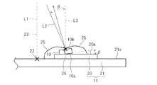
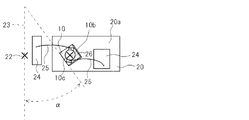
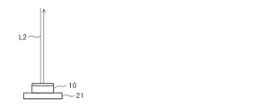
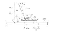
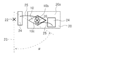
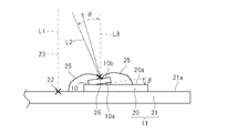
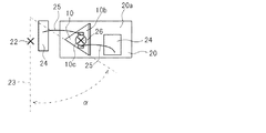
図2Aは、本実施形態に係る光受信モジュール1が備える受光素子10と受光素子支持部材11(サブマウント20及びステム21)の詳細の一例を示す正面図である。図2Bは、本実施形態に係る光受信モジュール1が備える受光素子10と受光素子支持部材11の詳細の一例を示す平面図である。図2Cは、本実施形態に係る光受信モジュール1に含まれる受光素子10と受光素子支持部材11の詳細の一例を示す左側面図である。
FIG. 2A is a front view showing an example of details of the
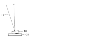
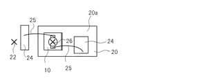
図3Aは、比較例の光受信モジュール1に含まれる受光素子10と受光素子支持部材11(サブマウント20及びステム21)の詳細を説明する正面図である。図3Bは、比較例の光受信モジュール1が備える受光素子10と受光素子支持部材11の詳細を説明する平面図である。図3Cは、比較例の光受信モジュール1が備える受光素子10と受光素子支持部材11の詳細を説明する左側面図である。
FIG. 3A is a front view illustrating details of the
本実施形態に係る光受信モジュール1では、サブマウント20の内側面(受光素子10を支持する受光素子支持面20a)とステム21の内側面(サブマウント20を支持するサブマウント支持面21a)とは、略平行である。そして、本実施形態に係る受光素子10は、四角柱形状をしている。そして、この受光素子10は光ファイバ3の光軸L1上の位置からずらして配置されている。また、本実施形態では、受光素子10の受光素子支持部材11側の面(本実施形態では、例えば、サブマウント側面10a)に含まれる複数の辺の方向はすべて、光の入射方向に直交する方向とは異なる方向に対応している。より具体的には、例えば、受光素子10のサブマウント側面10aに含まれる複数の辺それぞれについて、その辺を受光素子支持部材11の支持面(受光素子支持面20a又はサブマウント支持面21a)に投影した直線の方向が、入射光を受光素子支持部材11の支持面(受光素子支持面20a又はサブマウント支持面21a)に投影した直線に対して直交する方向とは異なる方向に対応している。
In the optical receiver module 1 according to the present embodiment, the inner surface of the submount 20 (light receiving
なお、本実施形態では、受光素子10のサブマウント側面10aは四角形状(一辺の長さが、例えば、0.4mm以下)である。また、本実施形態では、受光素子10の受光面10bとサブマウント側面10aとは略平行である。
In the present embodiment, the
また、本実施形態では、受光素子10のサブマウント側面10aに含まれる4つの辺すべてについて、その辺の、光ファイバ3の光軸L1と受光素子支持部材11(例えば、ステム21)の交点(光軸交点22)から、受光素子10が配置されている位置に向かう方向に対して垂直な平面(ずれ垂直面23)に対する角度の値は0ではない。本実施形態では、例えば、4つの辺のうちの、光ファイバ3の光軸L1から遠い側の辺の端の位置が、光ファイバ3の光軸L1に最も近い辺の、ずれ垂直面23に対する角度をα(αの値は0ではない。)とする。
In the present embodiment, for all four sides included in the
そして、この受光素子10の受光面10b及び受光素子支持部材11側の面(サブマウント側面10a)は、ステム21の内側面(又は、サブマウント20の内側面)に対して、光ファイバ3の光軸L1に向かって傾斜している。本実施形態では、例えば、受光素子10のサブマウント側面10aの、サブマウント20の支持面に対する角度をβとする。なお、サブマウント20をステム21に対して傾斜させることにより、受光素子10の受光面10bやサブマウント側面10aが、ステム21の内側面に対して傾斜するようにしてもよい。
The
受光素子10の受光面10bには受光部10cが設けられており、この受光部10cがレンズ13を通って入射する光信号を電気信号に変換する。そして、受光素子10は、ステム21上に設けられている電極24とワイヤ25により電気的に接続されており、電極24とリードピン4とは電気的に接続されている。
The
図2A、図2C、図3A及び図3Cには、光ファイバ3及びレンズ13を通って受光素子10に入射し、反射する光に対応する光線L2が示されている。そして、本実施形態に係る光受信モジュール1における、受光素子10に対する入射光の受光素子10の光ファイバ3の光軸に対する角度(受光素子10に対する入射光の受光素子支持部材11の支持面に対して垂直な方向L3からの角度)をθとする。
2A, 2C, 3A, and 3C show a light beam L2 corresponding to light that is incident on the
本実施形態に係る光受信モジュール1の製造工程は、受光素子10をサブマウント20に搭載する工程と、サブマウント20をステム21に搭載する工程とを含んでいる。そして、受光素子10とサブマウント20との接合、及び、サブマウント20とステム21との接合には、例えば、はんだや接着剤などが用いられる。
The manufacturing process of the optical receiver module 1 according to the present embodiment includes a process of mounting the
はんだや接着剤による接合では、光受信モジュール1の製造時に、はんだや接着剤の塗りむら(厚みのむら)が生じる可能性がある。そして、はんだや接着剤のむらによって、角度の組立て公差が発生する可能性がある。具体的には、例えば、はんだや接着剤層の厚みは一般的に10μm程度である。受光素子10は、サブマウント20の支持面の大きさに収まる大きさである必要がある点、及び、コストを低減することができる点、などの理由から、できるだけ小さくすることが望ましい。一方、受光素子10を小さくすると、はんだや接着剤のむらに伴う角度の公差が大きくなってしまう。例えば、受光素子10の一辺の長さが0.2mmであり、はんだや接着剤層の厚みを10μmの場合、上述の角度βは約3度(約0.05ラジアン)となる。一般的に、はんだや接着剤層の厚みが10μmを超えることも多い。また、受光素子10の一辺の長さが0.2mmよりも短いこともある。そのため、上述の角度βは10度に達する可能性がある。
In joining with solder or an adhesive, unevenness of coating of solder or adhesive (unevenness of thickness) may occur when the optical receiver module 1 is manufactured. In addition, the assembly tolerance of the angle may occur due to the unevenness of the solder or the adhesive. Specifically, for example, the thickness of the solder or adhesive layer is generally about 10 μm. It is desirable that the
そして、受光素子10をサブマウント20に押しつけることで、はんだや接着材による受光素子10とサブマウント20とを接合する。そのため、受光素子10のサブマウント側面10aに含まれる辺のうちのいずれかがサブマウント20に接する可能性が高い。そして、この押しつけの際に、サブマウント20に接する辺を軸とする角度の公差が発生することがある。
Then, by pressing the light receiving
このとき、例えば、図3A、図3B及び図3Cに示す比較例の光受信モジュール1のように、受光素子10のサブマウント側面10aに、光の入射方向に直交する方向に対応する方向の辺が含まれる場合は、上述の角度の公差により、光が受光素子10の受光面10bに対して垂直に入射して、反射戻り光が光ファイバ3に入射するよう受光素子10がサブマウント20上に搭載されてしまう可能性がある。
At this time, for example, as in the optical receiver module 1 of the comparative example shown in FIGS. 3A, 3B, and 3C, the side in the direction corresponding to the direction orthogonal to the incident direction of light on the
本実施形態に係る光受信モジュール1では、たとえ製造時に上述の角度の公差が発生しても、光が受光素子10の受光面10bに対して斜めに入射し、入射方向とは異なる方向に反射するので、反射戻り光が光ファイバ3に入射する可能性が低くなる。このようにして、反射減衰量が良好に保たれる。
In the optical receiver module 1 according to the present embodiment, even if the above-described angle tolerance occurs at the time of manufacture, light is incident on the
上述の説明のように、本実施形態に係る光受信モジュール1は、受光素子10の受光素子支持部材11側(例えば、サブマウント20側)の面に含まれる辺の方向が、光の入射方向に直交する方向とは異なる方向に対応しているので、図3A、図3B及び図3Cに示す比較例の光受信モジュール1と比較して、光受信モジュール1の製造時の角度の公差に伴う光ファイバ3に入射する反射戻り光の量の増加を抑制することができる。
As described above, in the optical receiver module 1 according to the present embodiment, the direction of the side included in the surface of the
また、本実施形態に係る光受信モジュール1では、光受信モジュール1の製造時の角度の公差の発生に伴う、光ファイバ3に入射する反射戻り光の量の増加を抑制することができるので、上述の角度θの値を小さく保って、受光効率を確保することも可能である。
Further, in the optical receiver module 1 according to the present embodiment, it is possible to suppress an increase in the amount of reflected return light incident on the
ここで、上述の角度β、及び、受光効率を確保するのに必要な角度θに基づいて、上述の角度αの値を算出する方法の一例を説明する。 Here, an example of a method for calculating the value of the angle α described above based on the angle β described above and the angle θ necessary for ensuring the light receiving efficiency will be described.
受光素子10の受光面10bに入射する光線L2と受光面10bとの交点(光線交点26)から光の入射方向に向かう光線ベクトルr(0,sinθ,cosθ)と、受光面10bの垂線ベクトルn(sinαsinβ,cosαsinβ,cosβ)と、の内積の値は、cos(sin−1(NA/2))以下となる。ここで、NAは、受光素子10に集光される光線の広がり角(1%となる値の広がり角度)を表す。NAについて1%となる値の広がり角度を採用すると、上述の関係は、受光素子10表面の反射率を一般的な値である2%とした場合に反射減衰量が−30dB程度以下となる関係となる。
A light vector r (0, sin θ, cos θ) from the intersection of the light beam L2 incident on the
上述の関係に基づいて、αの値は、cos−1((cos(sin−1(NA/2))−cosθcosβ)/sinθsinβ)以下であるという関係が導出される。αの値は、物理的にせいぜい1.05ラジアン(約60度)程度なので、このαの上限値に基づくと、θの値に関する以下の条件が導出される。
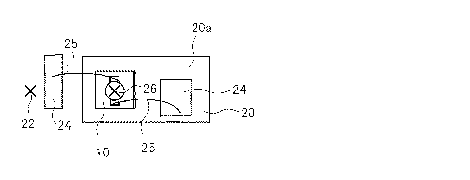
上述の説明のように、受光素子10のサブマウント20側の辺の方向が、受光効率(例えば、受光素子10に集光される光線の広がり角NA)と、受光素子10の受光面10bの受光素子支持部材11の支持面に対する傾きと、光の入射方向の光ファイバ3の光軸方向に対する傾きと、に基づいて特定される方向であってもよい。
As described above, the direction of the side of the
また、本実施形態に係る光受信モジュール1では、光軸交点22から、受光素子10が配置されている位置に向かう方向(ずれ方向)が、サブマウント20の長手方向に対応している。こうすれば、はんだや接着剤により、サブマウント20とステム21とを接合する際に、サブマウント20のステム21に対する角度の公差が、上述のずれ方向に略垂直な方向に発生しやすくなる。このとき、光軸交点22からサブマウント20をずらす長さを0.7mm以上に設定すれば、はんだや接着剤の厚みのむらが10μmとしてもサブマウント20のステム21に対する角度の公差は1度以内に収まる。
Further, in the optical receiver module 1 according to the present embodiment, the direction (shift direction) from the optical
また、サブマウント20については、絶縁部材による基板上に電気的なパタンを形成したものでも、集積回路素子でも構わない。
The
なお、本発明は上記実施形態に限定されるものではない。 The present invention is not limited to the above embodiment.
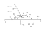
図4Aは、別の実施形態に係る光受信モジュール1が備える受光素子10と受光素子支持部材11(サブマウント20及びステム21)の詳細を説明する正面図である。図4Bは、図4Aに示す実施形態に係る光受信モジュール1が備える受光素子10と受光素子支持部材11の詳細を説明する平面図である。図4Aには光線L2が示されている。
FIG. 4A is a front view illustrating details of the
例えば、図4A及び図4Bに例示するように、受光素子10の受光素子支持部材11側の面(この実施形態ではサブマウント側面10a)が菱形形状であってもよい。具体的には、例えば、受光素子10が、菱形柱形状であっても構わない。そして、受光素子10の受光素子支持部材11側の面(この実施形態ではサブマウント側面10a)の対角線の方向が、光ファイバ3の光軸上の点を通る直線の方向に対応していてもよい。より具体的には、例えば、受光素子10の受光素子支持部材11側の面の対角線の延伸方向と、光ファイバ3の光軸の方向と、が交差するようにしてもよい。こうすれば、受光素子10が直方体形状である場合と比較して、上述の角度αの値のとれる範囲が広くなる。そのため、光受信モジュール1の製造時の角度の公差が発生に伴う、光ファイバ3に入射する反射戻り光の量の増加をより抑制することができる。
For example, as illustrated in FIG. 4A and FIG. 4B, the light receiving
図5Aは、さらに別の実施形態に係る光受信モジュール1が備える受光素子10と受光素子支持部材11(サブマウント20及びステム21)の詳細を説明する正面図である。図5Bは、図5Bに示す実施形態に係る光受信モジュール1が備える受光素子10と受光素子支持部材11の詳細を説明する平面図である。図5Aには、光線L2が示されている。
FIG. 5A is a front view illustrating details of the
図5A及び図5Bに示すように、受光素子10の受光素子支持部材11側の面(この実施形態ではサブマウント側面10a)が三角形状であってもよい。具体的には、例えば、受光素子10が三角柱状であってもよい。こうすれば、受光素子10が四角柱状である場合と比較して、上述の角度αの値のとれる範囲が広くなる。そのため、製造時の角度の公差が発生に伴う、光ファイバ3に入射する反射戻り光の量の増加をより抑制することができる。
As shown in FIGS. 5A and 5B, the surface of the
そして、図5A及び図5Bからわかるように、受光素子10の受光素子支持部材11側の面に含まれるすべての辺の方向が、入射光の方向に直交する方向とは異なる方向に対応している必要はない。具体的には、受光素子10の受光素子支持部材11側の面に含まれる辺のうちの、辺の延伸方向が光の入射方向に対応する直線と、光ファイバ3の光軸の方向に対応する直線と、受光素子支持部材11の受光素子10を支持する支持面と、に囲まれる領域に交差する辺の方向が、光の入射方向に直交する方向とは異なる方向に対応していればよい。
As can be seen from FIGS. 5A and 5B, the directions of all sides included in the surface of the
なお、本発明は上記実施形態にも限定されるものではない。 The present invention is not limited to the above embodiment.
例えば、本実施形態に係る光受信モジュール1が備える受光素子10が、受光素子支持部材11の支持面に対して傾斜していなくてもよい。また、ステム21の内側面とサブマウント20の内側面(受光素子10を支持する支持面)とが略平行でなくてもよい。また、受光素子10の受光面10bとサブマウント側面10aとが略平行でなくてもよい。また、受光素子10の受光面10bの形状とサブマウント側面10aの形状が異なっていてもよい。
For example, the
1 光受信モジュール、2 コネクタ、3 光ファイバ、4 リードピン、5 フレキシブル基板、10 受光素子、10a サブマウント側面、10b 受光面、10c 受光部、11 受光素子支持部材、12 搭載素子、13 レンズ、14 光レセプタクル、15 レンズ収容部、15a レンズ収容後部、15b レンズ収容前部、16 光ファイバ収容部、17a 凹部、17b 凹部、20 サブマウント、20a 受光素子支持面、21 ステム、21a サブマウント支持面、22 光軸交点、23 ずれ垂直面、24 電極、25 ワイヤ、26 光線交点。 DESCRIPTION OF SYMBOLS 1 Optical receiver module, 2 Connector, 3 Optical fiber, 4 Lead pin, 5 Flexible board, 10 Light receiving element, 10a Submount side surface, 10b Light receiving surface, 10c Light receiving part, 11 Light receiving element support member, 12 Mounting element, 13 Lens, 14 Optical receptacle, 15 Lens housing part, 15a Lens housing rear part, 15b Lens housing front part, 16 Optical fiber housing part, 17a Concave part, 17b Concave part, 20 Submount, 20a Light receiving element support surface, 21 Stem, 21a Submount support surface, 22 optical axis intersection, 23 deviation vertical plane, 24 electrodes, 25 wires, 26 ray intersection.
Claims (5)
受光素子と、前記受光素子を支持する支持部材と、を備え、
前記受光素子が、前記光ファイバの光軸上の位置からずらして配置されており、
前記受光素子の前記支持部材側の面に含まれる複数の辺のうちの、辺の延伸方向が、前記入射する光の方向に対応する直線と、前記光ファイバの光軸の方向に対応する直線と、前記支持部材の前記受光素子を支持する支持面と、に囲まれる領域に交差する交差辺の方向が、前記光の入射方向に直交する方向とは異なる方向に対応するよう前記受光素子が配置されている、
ことを特徴とする光受信モジュール。 An optical receiver module that receives light incident through an optical fiber to be connected,
A light receiving element, and a support member that supports the light receiving element,
The light receiving element is arranged shifted from a position on the optical axis of the optical fiber;
Of the plurality of sides included in the surface of the light receiving element on the support member side, the extending direction of the side corresponds to the straight line corresponding to the direction of the incident light and the straight line corresponding to the direction of the optical axis of the optical fiber. And the support surface of the support member that supports the light receiving element, and the direction of the intersecting side that intersects the region surrounded by the light receiving element corresponds to a direction different from the direction perpendicular to the light incident direction. Arranged,
An optical receiver module.
ことを特徴とする請求項1に記載の光受信モジュール。 The light receiving element is arranged such that the directions of all sides included in the surface of the light receiving element on the support member side correspond to a direction different from a direction orthogonal to the direction of the incident light. The optical receiver module according to claim 1.
ことを特徴とする請求項1又は2に記載の光受信モジュール。 The light receiving surface of the light receiving element is inclined in a direction toward the optical axis of the optical fiber with respect to the support surface of the support member.
The optical receiver module according to claim 1, wherein the optical receiver module is an optical receiver module.
ことを特徴とする請求項1から3のいずれか一項に記載の光受信モジュール。 The direction of the intersecting side of the light receiving element is the light receiving efficiency, the inclination of the light receiving surface of the light receiving element with respect to the support surface of the support member, and the inclination of the light incident direction with respect to the optical axis direction of the optical fiber. The direction identified based on the
The optical receiver module according to claim 1, wherein the optical receiver module is a light receiving module.
前記光ファイバの光軸上の位置からずらして、前記受光素子の前記支持部材側の面に含まれる複数の辺のうちの、辺の延伸方向が、前記入射する光の方向に対応する直線と、前記光ファイバの光軸の方向に対応する直線と、前記支持部材の前記受光素子を支持する支持面と、に囲まれる領域に交差する交差辺の方向が、前記光の入射方向に直交する方向とは異なる方向に対応するよう前記受光素子を配置する工程、
を含むことを特徴とする光受信モジュールの製造方法。 A light receiving module comprising a light receiving element and a support member that supports the light receiving element, and a method for manufacturing an optical receiving module that receives light incident through an optical fiber to be connected,
Shifting from the position on the optical axis of the optical fiber, the extending direction of the side of the plurality of sides included in the surface on the support member side of the light receiving element is a straight line corresponding to the direction of the incident light. The direction of the intersecting side that intersects the region surrounded by the straight line corresponding to the direction of the optical axis of the optical fiber and the support surface that supports the light receiving element of the support member is orthogonal to the incident direction of the light. Arranging the light receiving element to correspond to a direction different from the direction;
The manufacturing method of the optical receiver module characterized by including.
Priority Applications (2)
| Application Number | Priority Date | Filing Date | Title |
|---|---|---|---|
| JP2008315422A JP5135192B2 (en) | 2008-12-11 | 2008-12-11 | Optical receiver module and method of manufacturing optical receiver module |
| US12/622,965 US8378289B2 (en) | 2008-12-11 | 2009-11-20 | Optical receiver module and manufacturing method with a shifted and angled light receiving element |
Applications Claiming Priority (1)
| Application Number | Priority Date | Filing Date | Title |
|---|---|---|---|
| JP2008315422A JP5135192B2 (en) | 2008-12-11 | 2008-12-11 | Optical receiver module and method of manufacturing optical receiver module |
Publications (2)
| Publication Number | Publication Date |
|---|---|
| JP2010141089A true JP2010141089A (en) | 2010-06-24 |
| JP5135192B2 JP5135192B2 (en) | 2013-01-30 |
Family
ID=42239374
Family Applications (1)
| Application Number | Title | Priority Date | Filing Date |
|---|---|---|---|
| JP2008315422A Active JP5135192B2 (en) | 2008-12-11 | 2008-12-11 | Optical receiver module and method of manufacturing optical receiver module |
Country Status (2)
| Country | Link |
|---|---|
| US (1) | US8378289B2 (en) |
| JP (1) | JP5135192B2 (en) |
Cited By (3)
| Publication number | Priority date | Publication date | Assignee | Title |
|---|---|---|---|---|
| JP2012084714A (en) * | 2010-10-13 | 2012-04-26 | Opnext Japan Inc | Photodetector module |
| JP2014175605A (en) * | 2013-03-12 | 2014-09-22 | Seiko Instruments Inc | Light receiving sensor and manufacturing method of the same |
| US8987655B2 (en) | 2011-12-21 | 2015-03-24 | Oclaro Japan, Inc. | Optical module having at least one light receiving element with a wiring part covers a part of a side surface of a mesa part |
Families Citing this family (4)
| Publication number | Priority date | Publication date | Assignee | Title |
|---|---|---|---|---|
| US9754617B2 (en) | 2015-02-23 | 2017-09-05 | Seagate Technology Llc | Laser diode unit with enhanced thermal conduction to slider |
| WO2017115412A1 (en) * | 2015-12-28 | 2017-07-06 | オリンパス株式会社 | Optical transmission module and endoscope |
| JP6586656B2 (en) * | 2016-08-05 | 2019-10-09 | サンテック株式会社 | Detection device |
| CN109725391B (en) * | 2017-10-27 | 2022-03-01 | 住友电工光电子器件创新株式会社 | Receiver optical assembly and method of assembling the same |
Citations (3)
| Publication number | Priority date | Publication date | Assignee | Title |
|---|---|---|---|---|
| JPH10307236A (en) * | 1997-05-09 | 1998-11-17 | Mitsubishi Electric Corp | Optical semiconductor module |
| JP2001021775A (en) * | 1999-07-09 | 2001-01-26 | Sumitomo Electric Ind Ltd | Optical device |
| JP2006154534A (en) * | 2004-11-30 | 2006-06-15 | Oki Electric Ind Co Ltd | Manufacturing method for optical module and optical module |
Family Cites Families (6)
| Publication number | Priority date | Publication date | Assignee | Title |
|---|---|---|---|---|
| JP2765321B2 (en) | 1991-11-29 | 1998-06-11 | 日本電気株式会社 | Semiconductor light receiving element |
| JPH0894887A (en) | 1994-09-22 | 1996-04-12 | Japan Aviation Electron Ind Ltd | Optically coupled component and manufacturing method thereof |
| JPH08186321A (en) | 1994-12-28 | 1996-07-16 | Canon Inc | Semiconductor laser device |
| JP2003209268A (en) | 2002-01-11 | 2003-07-25 | Mitsubishi Electric Corp | Optical module |
| US6850674B2 (en) * | 2002-05-09 | 2005-02-01 | Sumitomo Electric Industries, Ltd. | Optical device |
| JP2005072130A (en) | 2003-08-21 | 2005-03-17 | Mitsubishi Electric Corp | Semiconductor laser device |
-
2008
- 2008-12-11 JP JP2008315422A patent/JP5135192B2/en active Active
-
2009
- 2009-11-20 US US12/622,965 patent/US8378289B2/en active Active
Patent Citations (3)
| Publication number | Priority date | Publication date | Assignee | Title |
|---|---|---|---|---|
| JPH10307236A (en) * | 1997-05-09 | 1998-11-17 | Mitsubishi Electric Corp | Optical semiconductor module |
| JP2001021775A (en) * | 1999-07-09 | 2001-01-26 | Sumitomo Electric Ind Ltd | Optical device |
| JP2006154534A (en) * | 2004-11-30 | 2006-06-15 | Oki Electric Ind Co Ltd | Manufacturing method for optical module and optical module |
Cited By (3)
| Publication number | Priority date | Publication date | Assignee | Title |
|---|---|---|---|---|
| JP2012084714A (en) * | 2010-10-13 | 2012-04-26 | Opnext Japan Inc | Photodetector module |
| US8987655B2 (en) | 2011-12-21 | 2015-03-24 | Oclaro Japan, Inc. | Optical module having at least one light receiving element with a wiring part covers a part of a side surface of a mesa part |
| JP2014175605A (en) * | 2013-03-12 | 2014-09-22 | Seiko Instruments Inc | Light receiving sensor and manufacturing method of the same |
Also Published As
| Publication number | Publication date |
|---|---|
| US20100148041A1 (en) | 2010-06-17 |
| JP5135192B2 (en) | 2013-01-30 |
| US8378289B2 (en) | 2013-02-19 |
Similar Documents
| Publication | Publication Date | Title |
|---|---|---|
| JP5135192B2 (en) | Optical receiver module and method of manufacturing optical receiver module | |
| JP3987500B2 (en) | Optical wiring board and method for manufacturing optical wiring board | |
| US9182551B2 (en) | Lens component and optical module provided with the same | |
| US20010041034A1 (en) | Substrate, optical fiber connection end member, optical element housing member, and method of fabrication of an optical module and the substrate | |
| JP5376617B2 (en) | Photoelectric conversion module | |
| EP3667378B1 (en) | Optical module | |
| US5617439A (en) | Semiconductor laser device and semiconductor laser array device | |
| US6921921B2 (en) | Light emitting modules | |
| JP7331727B2 (en) | Optical semiconductor device | |
| JP2012256692A (en) | Optical module | |
| JP2004020872A (en) | Optical semiconductor module | |
| US7866898B2 (en) | Optical communication module | |
| JP5605382B2 (en) | Optical module | |
| JP2020535488A (en) | Optical connectors, optical modules and clip members | |
| US20070201530A1 (en) | Optical active device and optical module using the same | |
| WO2018180786A1 (en) | Optical component and optical connector and optical module comprising same | |
| JP2001021769A (en) | Support for mounting an optoelectronic component and method of manufacturing the support | |
| JP2008224941A (en) | Optical module | |
| JP4360651B2 (en) | Optical module and manufacturing method thereof | |
| JP5853934B2 (en) | Optical module | |
| JP4821619B2 (en) | Optical module | |
| US20140198469A1 (en) | Electronic circuit, light source device, and method of manufacturing electronic circuit | |
| EP4485024A1 (en) | Optical waveguide substrate, optical waveguide package, and light source module | |
| JP6102652B2 (en) | Photoelectric conversion module | |
| TW202546490A (en) | Optical connector cable |
Legal Events
| Date | Code | Title | Description |
|---|---|---|---|
| A621 | Written request for application examination |
Free format text: JAPANESE INTERMEDIATE CODE: A621 Effective date: 20101214 |
|
| A977 | Report on retrieval |
Free format text: JAPANESE INTERMEDIATE CODE: A971007 Effective date: 20120112 |
|
| A131 | Notification of reasons for refusal |
Free format text: JAPANESE INTERMEDIATE CODE: A131 Effective date: 20120703 |
|
| A521 | Request for written amendment filed |
Free format text: JAPANESE INTERMEDIATE CODE: A523 Effective date: 20120806 |
|
| A131 | Notification of reasons for refusal |
Free format text: JAPANESE INTERMEDIATE CODE: A131 Effective date: 20120821 |
|
| A521 | Request for written amendment filed |
Free format text: JAPANESE INTERMEDIATE CODE: A523 Effective date: 20121004 |
|
| TRDD | Decision of grant or rejection written | ||
| A01 | Written decision to grant a patent or to grant a registration (utility model) |
Free format text: JAPANESE INTERMEDIATE CODE: A01 Effective date: 20121023 |
|
| A01 | Written decision to grant a patent or to grant a registration (utility model) |
Free format text: JAPANESE INTERMEDIATE CODE: A01 |
|
| A61 | First payment of annual fees (during grant procedure) |
Free format text: JAPANESE INTERMEDIATE CODE: A61 Effective date: 20121112 |
|
| FPAY | Renewal fee payment (event date is renewal date of database) |
Free format text: PAYMENT UNTIL: 20151116 Year of fee payment: 3 |
|
| R150 | Certificate of patent or registration of utility model |
Free format text: JAPANESE INTERMEDIATE CODE: R150 Ref document number: 5135192 Country of ref document: JP Free format text: JAPANESE INTERMEDIATE CODE: R150 |
|
| S531 | Written request for registration of change of domicile |
Free format text: JAPANESE INTERMEDIATE CODE: R313531 |
|
| R350 | Written notification of registration of transfer |
Free format text: JAPANESE INTERMEDIATE CODE: R350 |
|
| R250 | Receipt of annual fees |
Free format text: JAPANESE INTERMEDIATE CODE: R250 |
|
| R250 | Receipt of annual fees |
Free format text: JAPANESE INTERMEDIATE CODE: R250 |
|
| R250 | Receipt of annual fees |
Free format text: JAPANESE INTERMEDIATE CODE: R250 |
|
| R250 | Receipt of annual fees |
Free format text: JAPANESE INTERMEDIATE CODE: R250 |
|
| S533 | Written request for registration of change of name |
Free format text: JAPANESE INTERMEDIATE CODE: R313533 |
|
| R350 | Written notification of registration of transfer |
Free format text: JAPANESE INTERMEDIATE CODE: R350 |
|
| R250 | Receipt of annual fees |
Free format text: JAPANESE INTERMEDIATE CODE: R250 |
|
| R250 | Receipt of annual fees |
Free format text: JAPANESE INTERMEDIATE CODE: R250 |
|
| R250 | Receipt of annual fees |
Free format text: JAPANESE INTERMEDIATE CODE: R250 |
|
| R250 | Receipt of annual fees |
Free format text: JAPANESE INTERMEDIATE CODE: R250 |
|
| R250 | Receipt of annual fees |
Free format text: JAPANESE INTERMEDIATE CODE: R250 |
|
| R250 | Receipt of annual fees |
Free format text: JAPANESE INTERMEDIATE CODE: R250 |
|
| R250 | Receipt of annual fees |
Free format text: JAPANESE INTERMEDIATE CODE: R250 |