JP2010141089A - 光受信モジュール及び光受信モジュールの製造方法 - Google Patents
光受信モジュール及び光受信モジュールの製造方法 Download PDFInfo
- Publication number
- JP2010141089A JP2010141089A JP2008315422A JP2008315422A JP2010141089A JP 2010141089 A JP2010141089 A JP 2010141089A JP 2008315422 A JP2008315422 A JP 2008315422A JP 2008315422 A JP2008315422 A JP 2008315422A JP 2010141089 A JP2010141089 A JP 2010141089A
- Authority
- JP
- Japan
- Prior art keywords
- light receiving
- receiving element
- light
- optical
- support member
- Prior art date
- Legal status (The legal status is an assumption and is not a legal conclusion. Google has not performed a legal analysis and makes no representation as to the accuracy of the status listed.)
- Granted
Links
Images

Classifications
-
- G—PHYSICS
- G02—OPTICS
- G02B—OPTICAL ELEMENTS, SYSTEMS OR APPARATUS
- G02B6/00—Light guides; Structural details of arrangements comprising light guides and other optical elements, e.g. couplings
- G02B6/24—Coupling light guides
- G02B6/42—Coupling light guides with opto-electronic elements
- G02B6/4201—Packages, e.g. shape, construction, internal or external details
- G02B6/4202—Packages, e.g. shape, construction, internal or external details for coupling an active element with fibres without intermediate optical elements, e.g. fibres with plane ends, fibres with shaped ends, bundles
- G02B6/4203—Optical features
-
- Y—GENERAL TAGGING OF NEW TECHNOLOGICAL DEVELOPMENTS; GENERAL TAGGING OF CROSS-SECTIONAL TECHNOLOGIES SPANNING OVER SEVERAL SECTIONS OF THE IPC; TECHNICAL SUBJECTS COVERED BY FORMER USPC CROSS-REFERENCE ART COLLECTIONS [XRACs] AND DIGESTS
- Y10—TECHNICAL SUBJECTS COVERED BY FORMER USPC
- Y10T—TECHNICAL SUBJECTS COVERED BY FORMER US CLASSIFICATION
- Y10T29/00—Metal working
- Y10T29/49—Method of mechanical manufacture
- Y10T29/49826—Assembling or joining
Landscapes
- Physics & Mathematics (AREA)
- General Physics & Mathematics (AREA)
- Optics & Photonics (AREA)
- Optical Couplings Of Light Guides (AREA)
- Light Receiving Elements (AREA)
- Die Bonding (AREA)
Abstract
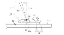
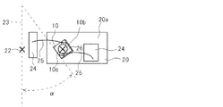
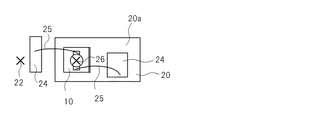
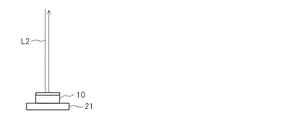
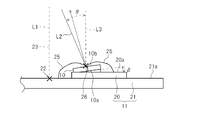
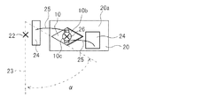
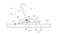
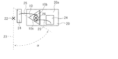
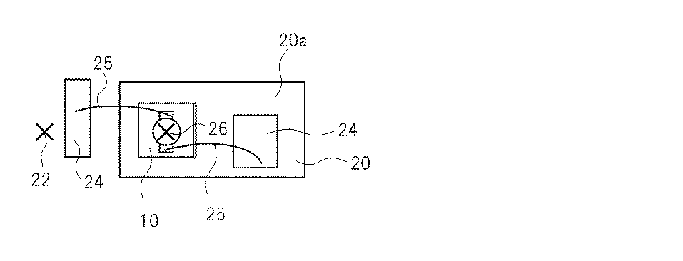
【解決手段】光受信モジュールは、受光素子10と、受光素子10を支持するサブマウント20と、を備える。受光素子10は、光ファイバの光軸上の位置からずらして配置されている。受光素子10のサブマウント20側の面に含まれる複数の辺のうちの、辺の延伸方向が、入射する光の方向に対応する直線と、光ファイバの光軸の方向に対応する直線と、支持部材の前記受光素子を支持する支持面と、に囲まれる領域に交差する交差辺の方向が、光の入射方向に直交する方向とは異なる方向に対応するよう受光素子10が配置されている。
【選択図】図2B
Description
Claims (5)
- 接続される光ファイバを通って入射する光を受け付ける光受信モジュールであって、
受光素子と、前記受光素子を支持する支持部材と、を備え、
前記受光素子が、前記光ファイバの光軸上の位置からずらして配置されており、
前記受光素子の前記支持部材側の面に含まれる複数の辺のうちの、辺の延伸方向が、前記入射する光の方向に対応する直線と、前記光ファイバの光軸の方向に対応する直線と、前記支持部材の前記受光素子を支持する支持面と、に囲まれる領域に交差する交差辺の方向が、前記光の入射方向に直交する方向とは異なる方向に対応するよう前記受光素子が配置されている、
ことを特徴とする光受信モジュール。 - 前記受光素子の前記支持部材側の面に含まれるすべての辺の方向が、前記入射する光の方向に直交する方向とは異なる方向に対応するよう前記受光素子が配置されている
ことを特徴とする請求項1に記載の光受信モジュール。 - 前記受光素子の受光面が、前記支持部材の前記支持面に対して、前記光ファイバの光軸に向かう方向に傾斜している、
ことを特徴とする請求項1又は2に記載の光受信モジュール。 - 前記受光素子の前記交差辺の方向が、受光効率と、前記受光素子の受光面の前記支持部材の支持面に対する傾きと、前記光の入射方向の前記光ファイバの光軸方向に対する傾きと、に基づいて特定される方向である、
ことを特徴とする請求項1から3のいずれか一項に記載の光受信モジュール。 - 受光素子と、前記受光素子を支持する支持部材と、を備える、接続される光ファイバを通って入射する光を受け付ける光受信モジュールの製造方法であって、
前記光ファイバの光軸上の位置からずらして、前記受光素子の前記支持部材側の面に含まれる複数の辺のうちの、辺の延伸方向が、前記入射する光の方向に対応する直線と、前記光ファイバの光軸の方向に対応する直線と、前記支持部材の前記受光素子を支持する支持面と、に囲まれる領域に交差する交差辺の方向が、前記光の入射方向に直交する方向とは異なる方向に対応するよう前記受光素子を配置する工程、
を含むことを特徴とする光受信モジュールの製造方法。
Priority Applications (2)
| Application Number | Priority Date | Filing Date | Title |
|---|---|---|---|
| JP2008315422A JP5135192B2 (ja) | 2008-12-11 | 2008-12-11 | 光受信モジュール及び光受信モジュールの製造方法 |
| US12/622,965 US8378289B2 (en) | 2008-12-11 | 2009-11-20 | Optical receiver module and manufacturing method with a shifted and angled light receiving element |
Applications Claiming Priority (1)
| Application Number | Priority Date | Filing Date | Title |
|---|---|---|---|
| JP2008315422A JP5135192B2 (ja) | 2008-12-11 | 2008-12-11 | 光受信モジュール及び光受信モジュールの製造方法 |
Publications (2)
| Publication Number | Publication Date |
|---|---|
| JP2010141089A true JP2010141089A (ja) | 2010-06-24 |
| JP5135192B2 JP5135192B2 (ja) | 2013-01-30 |
Family
ID=42239374
Family Applications (1)
| Application Number | Title | Priority Date | Filing Date |
|---|---|---|---|
| JP2008315422A Active JP5135192B2 (ja) | 2008-12-11 | 2008-12-11 | 光受信モジュール及び光受信モジュールの製造方法 |
Country Status (2)
| Country | Link |
|---|---|
| US (1) | US8378289B2 (ja) |
| JP (1) | JP5135192B2 (ja) |
Cited By (3)
| Publication number | Priority date | Publication date | Assignee | Title |
|---|---|---|---|---|
| JP2012084714A (ja) * | 2010-10-13 | 2012-04-26 | Opnext Japan Inc | 受光モジュール |
| JP2014175605A (ja) * | 2013-03-12 | 2014-09-22 | Seiko Instruments Inc | 受光センサ及び受光センサの製造方法 |
| US8987655B2 (en) | 2011-12-21 | 2015-03-24 | Oclaro Japan, Inc. | Optical module having at least one light receiving element with a wiring part covers a part of a side surface of a mesa part |
Families Citing this family (4)
| Publication number | Priority date | Publication date | Assignee | Title |
|---|---|---|---|---|
| US9754617B2 (en) * | 2015-02-23 | 2017-09-05 | Seagate Technology Llc | Laser diode unit with enhanced thermal conduction to slider |
| WO2017115412A1 (ja) * | 2015-12-28 | 2017-07-06 | オリンパス株式会社 | 光伝送モジュールおよび内視鏡 |
| JP6586656B2 (ja) * | 2016-08-05 | 2019-10-09 | サンテック株式会社 | 検出装置 |
| CN109725391B (zh) * | 2017-10-27 | 2022-03-01 | 住友电工光电子器件创新株式会社 | 接收器光学组件及其组装方法 |
Citations (3)
| Publication number | Priority date | Publication date | Assignee | Title |
|---|---|---|---|---|
| JPH10307236A (ja) * | 1997-05-09 | 1998-11-17 | Mitsubishi Electric Corp | 光半導体モジュール |
| JP2001021775A (ja) * | 1999-07-09 | 2001-01-26 | Sumitomo Electric Ind Ltd | 光学装置 |
| JP2006154534A (ja) * | 2004-11-30 | 2006-06-15 | Oki Electric Ind Co Ltd | 光モジュールの製造方法,および,光モジュール |
Family Cites Families (6)
| Publication number | Priority date | Publication date | Assignee | Title |
|---|---|---|---|---|
| JP2765321B2 (ja) | 1991-11-29 | 1998-06-11 | 日本電気株式会社 | 半導体受光素子 |
| JPH0894887A (ja) | 1994-09-22 | 1996-04-12 | Japan Aviation Electron Ind Ltd | 光結合部品およびその製造方法 |
| JPH08186321A (ja) | 1994-12-28 | 1996-07-16 | Canon Inc | 半導体レーザ装置 |
| JP2003209268A (ja) | 2002-01-11 | 2003-07-25 | Mitsubishi Electric Corp | 光モジュール |
| KR20040111587A (ko) * | 2002-05-09 | 2004-12-31 | 스미토모 덴키 고교 가부시키가이샤 | 광 디바이스 |
| JP2005072130A (ja) | 2003-08-21 | 2005-03-17 | Mitsubishi Electric Corp | 半導体レーザ装置 |
-
2008
- 2008-12-11 JP JP2008315422A patent/JP5135192B2/ja active Active
-
2009
- 2009-11-20 US US12/622,965 patent/US8378289B2/en active Active
Patent Citations (3)
| Publication number | Priority date | Publication date | Assignee | Title |
|---|---|---|---|---|
| JPH10307236A (ja) * | 1997-05-09 | 1998-11-17 | Mitsubishi Electric Corp | 光半導体モジュール |
| JP2001021775A (ja) * | 1999-07-09 | 2001-01-26 | Sumitomo Electric Ind Ltd | 光学装置 |
| JP2006154534A (ja) * | 2004-11-30 | 2006-06-15 | Oki Electric Ind Co Ltd | 光モジュールの製造方法,および,光モジュール |
Cited By (3)
| Publication number | Priority date | Publication date | Assignee | Title |
|---|---|---|---|---|
| JP2012084714A (ja) * | 2010-10-13 | 2012-04-26 | Opnext Japan Inc | 受光モジュール |
| US8987655B2 (en) | 2011-12-21 | 2015-03-24 | Oclaro Japan, Inc. | Optical module having at least one light receiving element with a wiring part covers a part of a side surface of a mesa part |
| JP2014175605A (ja) * | 2013-03-12 | 2014-09-22 | Seiko Instruments Inc | 受光センサ及び受光センサの製造方法 |
Also Published As
| Publication number | Publication date |
|---|---|
| JP5135192B2 (ja) | 2013-01-30 |
| US20100148041A1 (en) | 2010-06-17 |
| US8378289B2 (en) | 2013-02-19 |
Similar Documents
| Publication | Publication Date | Title |
|---|---|---|
| JP5135192B2 (ja) | 光受信モジュール及び光受信モジュールの製造方法 | |
| JP3987500B2 (ja) | 光配線基板および光配線基板の製造方法 | |
| US20010041034A1 (en) | Substrate, optical fiber connection end member, optical element housing member, and method of fabrication of an optical module and the substrate | |
| JP5376617B2 (ja) | 光電変換モジュール | |
| JP2013200550A (ja) | レンズ部品及びそれを備えた光モジュール | |
| US6799901B2 (en) | Optical semiconductor module | |
| EP3667378B1 (en) | Optical module | |
| US6921921B2 (en) | Light emitting modules | |
| JP7331727B2 (ja) | 光半導体デバイス | |
| CN110573920A (zh) | 光子组件及其制造方法 | |
| JP3802844B2 (ja) | 光半導体モジュール | |
| JP2012256692A (ja) | 光モジュール | |
| US7866898B2 (en) | Optical communication module | |
| JP2020535488A (ja) | 光コネクタ、光モジュール及びクリップ部材 | |
| JP2013171112A (ja) | 光モジュール | |
| WO2018180786A1 (ja) | 光学部品、ならびにこれを備えた光コネクタおよび光モジュール | |
| JP2001021769A (ja) | 光電的な構成部材を取り付けるための支持体ならびにこの支持体を製造する方法 | |
| JP2008224941A (ja) | 光モジュール | |
| JP4360651B2 (ja) | 光モジュール及びその製造方法 | |
| US9332655B2 (en) | Electronic circuit, light source device, and method of manufacturing electronic circuit | |
| EP4485024A1 (en) | Optical waveguide substrate, optical waveguide package, and light source module | |
| JP6102652B2 (ja) | 光電変換モジュール | |
| TW202546490A (zh) | 光連接器纜線 | |
| JP7210120B2 (ja) | 光結合構造、光結合法方法、カメラモジュール | |
| JP5861753B2 (ja) | 光モジュール |
Legal Events
| Date | Code | Title | Description |
|---|---|---|---|
| A621 | Written request for application examination |
Free format text: JAPANESE INTERMEDIATE CODE: A621 Effective date: 20101214 |
|
| A977 | Report on retrieval |
Free format text: JAPANESE INTERMEDIATE CODE: A971007 Effective date: 20120112 |
|
| A131 | Notification of reasons for refusal |
Free format text: JAPANESE INTERMEDIATE CODE: A131 Effective date: 20120703 |
|
| A521 | Request for written amendment filed |
Free format text: JAPANESE INTERMEDIATE CODE: A523 Effective date: 20120806 |
|
| A131 | Notification of reasons for refusal |
Free format text: JAPANESE INTERMEDIATE CODE: A131 Effective date: 20120821 |
|
| A521 | Request for written amendment filed |
Free format text: JAPANESE INTERMEDIATE CODE: A523 Effective date: 20121004 |
|
| TRDD | Decision of grant or rejection written | ||
| A01 | Written decision to grant a patent or to grant a registration (utility model) |
Free format text: JAPANESE INTERMEDIATE CODE: A01 Effective date: 20121023 |
|
| A01 | Written decision to grant a patent or to grant a registration (utility model) |
Free format text: JAPANESE INTERMEDIATE CODE: A01 |
|
| A61 | First payment of annual fees (during grant procedure) |
Free format text: JAPANESE INTERMEDIATE CODE: A61 Effective date: 20121112 |
|
| FPAY | Renewal fee payment (event date is renewal date of database) |
Free format text: PAYMENT UNTIL: 20151116 Year of fee payment: 3 |
|
| R150 | Certificate of patent or registration of utility model |
Free format text: JAPANESE INTERMEDIATE CODE: R150 Ref document number: 5135192 Country of ref document: JP Free format text: JAPANESE INTERMEDIATE CODE: R150 |
|
| S531 | Written request for registration of change of domicile |
Free format text: JAPANESE INTERMEDIATE CODE: R313531 |
|
| R350 | Written notification of registration of transfer |
Free format text: JAPANESE INTERMEDIATE CODE: R350 |
|
| R250 | Receipt of annual fees |
Free format text: JAPANESE INTERMEDIATE CODE: R250 |
|
| R250 | Receipt of annual fees |
Free format text: JAPANESE INTERMEDIATE CODE: R250 |
|
| R250 | Receipt of annual fees |
Free format text: JAPANESE INTERMEDIATE CODE: R250 |
|
| R250 | Receipt of annual fees |
Free format text: JAPANESE INTERMEDIATE CODE: R250 |
|
| S533 | Written request for registration of change of name |
Free format text: JAPANESE INTERMEDIATE CODE: R313533 |
|
| R350 | Written notification of registration of transfer |
Free format text: JAPANESE INTERMEDIATE CODE: R350 |
|
| R250 | Receipt of annual fees |
Free format text: JAPANESE INTERMEDIATE CODE: R250 |
|
| R250 | Receipt of annual fees |
Free format text: JAPANESE INTERMEDIATE CODE: R250 |
|
| R250 | Receipt of annual fees |
Free format text: JAPANESE INTERMEDIATE CODE: R250 |
|
| R250 | Receipt of annual fees |
Free format text: JAPANESE INTERMEDIATE CODE: R250 |
|
| R250 | Receipt of annual fees |
Free format text: JAPANESE INTERMEDIATE CODE: R250 |
|
| R250 | Receipt of annual fees |
Free format text: JAPANESE INTERMEDIATE CODE: R250 |
|
| R250 | Receipt of annual fees |
Free format text: JAPANESE INTERMEDIATE CODE: R250 |