JP2010141187A - 半導体集積回路装置 - Google Patents
半導体集積回路装置 Download PDFInfo
- Publication number
- JP2010141187A JP2010141187A JP2008316965A JP2008316965A JP2010141187A JP 2010141187 A JP2010141187 A JP 2010141187A JP 2008316965 A JP2008316965 A JP 2008316965A JP 2008316965 A JP2008316965 A JP 2008316965A JP 2010141187 A JP2010141187 A JP 2010141187A
- Authority
- JP
- Japan
- Prior art keywords
- tap
- wiring
- integrated circuit
- semiconductor integrated
- cell
- Prior art date
- Legal status (The legal status is an assumption and is not a legal conclusion. Google has not performed a legal analysis and makes no representation as to the accuracy of the status listed.)
- Granted
Links
Images


Classifications
-
- H—ELECTRICITY
- H10—SEMICONDUCTOR DEVICES; ELECTRIC SOLID-STATE DEVICES NOT OTHERWISE PROVIDED FOR
- H10D—INORGANIC ELECTRIC SEMICONDUCTOR DEVICES
- H10D89/00—Aspects of integrated devices not covered by groups H10D84/00 - H10D88/00
- H10D89/10—Integrated device layouts
-
- H—ELECTRICITY
- H10—SEMICONDUCTOR DEVICES; ELECTRIC SOLID-STATE DEVICES NOT OTHERWISE PROVIDED FOR
- H10D—INORGANIC ELECTRIC SEMICONDUCTOR DEVICES
- H10D84/00—Integrated devices formed in or on semiconductor substrates that comprise only semiconducting layers, e.g. on Si wafers or on GaAs-on-Si wafers
- H10D84/90—Masterslice integrated circuits
- H10D84/903—Masterslice integrated circuits comprising field effect technology
- H10D84/907—CMOS gate arrays
-
- H—ELECTRICITY
- H10—SEMICONDUCTOR DEVICES; ELECTRIC SOLID-STATE DEVICES NOT OTHERWISE PROVIDED FOR
- H10W—GENERIC PACKAGES, INTERCONNECTIONS, CONNECTORS OR OTHER CONSTRUCTIONAL DETAILS OF DEVICES COVERED BY CLASS H10
- H10W20/00—Interconnections in chips, wafers or substrates
- H10W20/40—Interconnections external to wafers or substrates, e.g. back-end-of-line [BEOL] metallisations or vias connecting to gate electrodes
- H10W20/41—Interconnections external to wafers or substrates, e.g. back-end-of-line [BEOL] metallisations or vias connecting to gate electrodes characterised by their conductive parts
- H10W20/427—Power or ground buses
Landscapes
- Design And Manufacture Of Integrated Circuits (AREA)
Abstract
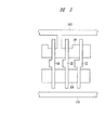
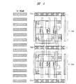
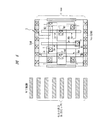
【解決手段】電源電位Vddを供給し、第1方向に沿って形成された第1タップと、電源電位Vssを供給し、第1方向と交差する第2方向に第1タップと対向して配置され、第1方向に沿って形成された第2タップと、第1タップと第2タップとの間に形成されたスタンダードセル3において、第2方向における第1タップの中心と第2方向における第2タップの中心との間のセルの高さ(距離L)を[(整数+0.5)×第2層目の配線の配線ピッチ]または[(整数+0.25)×第2層目の配線の配線ピッチ]とする。
【選択図】図2
Description
本実施の形態1に用いるスタンダードセルを構成する原始的回路とは、基本論理回路または基本機能回路であって、例えばNAND、NOR、EOR(Exclusive OR:XOR)、ENOR、フリップフロップ(Flip/Flop)、マルチプレクサ(Multiplexer)、インバータ(Inverter)、バッファ(Buffer)などである。
本実施の形態2は、前述の実施の形態1のセルの高さを(整数+0.25)×配線ピッチとした場合を示している。
2 機能装置
3 スタンダードセル
4 原始的回路
5a,5b,5c pチャネル型MISFET
6a,6b,6c nチャネル型MISFET
7 コンタクトホール
8 素子分離領域
9 シリサイド膜
10 層間絶縁膜
11 プラグ
12 層間絶縁膜
100 タップ
GE ゲート電極
GND 基準電位
L 距離(セルの高さ)
M1 第1層目の配線
M2 第2層目の配線
n+ 高濃度n型半導体領域
NiSO n型半導体領域
NW n型ウェル領域
p−sub p型半導体基板
p+ 高濃度p型半導体領域
PW p型ウェル領域
Vdd 電源電位
Vss 電源電位
Claims (12)
- 第1電位を供給し、第1方向に沿って形成された第1タップと、
前記第1電位と異なる電位である第2電位を供給し、前記第1方向と交差する第2方向に前記第1タップと対向して配置され、前記第1方向に沿って形成された第2タップと、
前記第2方向における前記第1タップの中心と、前記第2方向における前記第2タップの中心との間に形成されたスタンダードセルとを複数配列して構成されるセルアレイと、
前記第1タップ、前記第2タップおよび前記セルアレイ上に形成された複数層の配線とを含む半導体集積回路装置であって、
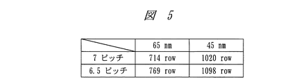
前記第1タップと前記第2タップとの間のセルの高さを[(整数+0.5)×前記複数層の配線のうち第2層目の配線の配線ピッチ]とすることを特徴とする半導体集積回路装置。 - 請求項1記載の半導体集積回路装置において、前記整数は、前記第1タップと前記第2タップとの間を通過できる前記第1方向に沿って形成された第2層目以上の配線の本数であることを特徴とする半導体集積回路装置。
- 請求項1記載の半導体集積回路装置において、前記第1電位は電源電位、前記第2電位は接地電位であることを特徴とする半導体集積回路装置。
- 請求項1記載の半導体集積回路装置において、前記配線ピッチは、最小加工寸法で形成された配線の幅と最小加工寸法で形成された配線の間隔とを足した最小配線ピッチであることを特徴とする半導体集積回路装置。
- 請求項1記載の半導体集積回路装置において、前記スタンダードセル内は前記複数層の配線のうち第1層目の配線により結線されていることを特徴とする半導体集積回路装置。
- 請求項1記載の半導体集積回路装置において、前記セルアレイは、前記スタンダードセルを複数有し、
前記複数のスタンダードセルの相互間は第2層目以上の配線により結線されていることを特徴とする半導体集積回路装置。 - 第1電位を供給し、第1方向に沿って形成された第1タップと、
前記第1電位と異なる電位である第2電位を供給し、前記第1方向と交差する第2方向に前記第1タップと対向して配置され、前記第1方向に沿って形成された第2タップと、
前記第2方向における前記第1タップの中心と、前記第2方向における前記第2タップの中心との間に形成されたスタンダードセルとを複数配列して構成されるセルアレイと、
前記第1タップ、前記第2タップおよび前記セルアレイ上に形成された複数層の配線とを含む半導体集積回路装置であって、
前記第1タップと前記第2タップとの間のセルの高さを[(整数+0.25)×前記複数層の配線のうち第2層目の配線の配線ピッチ]とすることを特徴とする半導体集積回路装置。 - 請求項7記載の半導体集積回路装置において、前記整数は、前記第1タップと前記第2タップとの間を通過できる前記第1方向に沿って形成された第2層目以上の配線の本数であることを特徴とする半導体集積回路装置。
- 請求項7記載の半導体集積回路装置において、前記第1電位は電源電位、前記第2電位は接地電位であることを特徴とする半導体集積回路装置。
- 請求項7記載の半導体集積回路装置において、前記配線ピッチは、最小加工寸法で形成された配線の幅と最小加工寸法で形成された配線の間隔とを足した最小配線ピッチであることを特徴とする半導体集積回路装置。
- 請求項7記載の半導体集積回路装置において、前記スタンダードセル内は前記複数層の配線のうち第1層目の配線により結線されていることを特徴とする半導体集積回路装置。
- 請求項7記載の半導体集積回路装置において、前記セルアレイは、前記スタンダードセルを複数有し、
前記複数のスタンダードセルの相互間は第2層目以上の配線により結線されていることを特徴とする半導体集積回路装置。
Priority Applications (3)
| Application Number | Priority Date | Filing Date | Title |
|---|---|---|---|
| JP2008316965A JP5410082B2 (ja) | 2008-12-12 | 2008-12-12 | 半導体集積回路装置 |
| US12/632,088 US8183600B2 (en) | 2008-12-12 | 2009-12-07 | Semiconductor integrated circuit device with reduced cell size |
| US13/461,612 US8410526B2 (en) | 2008-12-12 | 2012-05-01 | Semiconductor integrated circuit device with reduced cell size |
Applications Claiming Priority (1)
| Application Number | Priority Date | Filing Date | Title |
|---|---|---|---|
| JP2008316965A JP5410082B2 (ja) | 2008-12-12 | 2008-12-12 | 半導体集積回路装置 |
Publications (2)
| Publication Number | Publication Date |
|---|---|
| JP2010141187A true JP2010141187A (ja) | 2010-06-24 |
| JP5410082B2 JP5410082B2 (ja) | 2014-02-05 |
Family
ID=42239462
Family Applications (1)
| Application Number | Title | Priority Date | Filing Date |
|---|---|---|---|
| JP2008316965A Expired - Fee Related JP5410082B2 (ja) | 2008-12-12 | 2008-12-12 | 半導体集積回路装置 |
Country Status (2)
| Country | Link |
|---|---|
| US (2) | US8183600B2 (ja) |
| JP (1) | JP5410082B2 (ja) |
Cited By (5)
| Publication number | Priority date | Publication date | Assignee | Title |
|---|---|---|---|---|
| JP2014220498A (ja) * | 2013-05-02 | 2014-11-20 | 台湾積體電路製造股▲ふん▼有限公司Taiwan Semiconductor Manufacturing Company,Ltd. | 公称最小ピッチの非整数倍であるセル高さを有するスタンダードセル |
| KR20180020122A (ko) | 2015-06-24 | 2018-02-27 | 르네사스 일렉트로닉스 가부시키가이샤 | 반도체 장치 |
| WO2019003840A1 (ja) * | 2017-06-27 | 2019-01-03 | 株式会社ソシオネクスト | 半導体集積回路装置 |
| KR20190045911A (ko) * | 2016-09-15 | 2019-05-03 | 퀄컴 인코포레이티드 | 감소된 영역을 위한 최소 트랙 표준 셀 회로들 |
| JPWO2022172737A1 (ja) * | 2021-02-15 | 2022-08-18 |
Families Citing this family (33)
| Publication number | Priority date | Publication date | Assignee | Title |
|---|---|---|---|---|
| US8350340B1 (en) * | 2011-08-05 | 2013-01-08 | Himax Technologies Limited | Structure of output stage |
| TWI473420B (zh) * | 2011-09-15 | 2015-02-11 | Himax Tech Ltd | 輸出級的結構 |
| US8698205B2 (en) * | 2012-05-25 | 2014-04-15 | Taiwan Semiconductor Manufacturing Company, Ltd. | Integrated circuit layout having mixed track standard cell |
| CN104134657B (zh) * | 2013-05-02 | 2018-01-26 | 台湾积体电路制造股份有限公司 | 单元高度为标称最小间距的非整数倍的标准单元 |
| KR102083388B1 (ko) | 2013-09-24 | 2020-03-02 | 삼성전자주식회사 | 반도체 소자 및 그 제조 방법 |
| US9483600B2 (en) | 2014-03-14 | 2016-11-01 | Qualcomm Incorporated | Multi supply cell arrays for low power designs |
| US9385726B2 (en) * | 2014-04-17 | 2016-07-05 | Infineon Technologies Ag | Chip and method for manufacturing a chip |
| KR102349417B1 (ko) * | 2015-07-16 | 2022-01-10 | 삼성전자 주식회사 | 전압 강하를 개선할 수 있는 구조를 갖는 반도체 장치와 이를 포함하는 장치 |
| US10068918B2 (en) | 2015-09-21 | 2018-09-04 | Globalfoundries Inc. | Contacting SOI subsrates |
| US9793211B2 (en) * | 2015-10-20 | 2017-10-17 | Taiwan Semiconductor Manufacturing Co., Ltd. | Dual power structure with connection pins |
| WO2017145906A1 (ja) * | 2016-02-25 | 2017-08-31 | 株式会社ソシオネクスト | 半導体集積回路装置 |
| US11189569B2 (en) | 2016-09-23 | 2021-11-30 | Advanced Micro Devices, Inc. | Power grid layout designs for integrated circuits |
| US10127340B2 (en) | 2016-09-30 | 2018-11-13 | Taiwan Semiconductor Manufacturing Company, Ltd. | Standard cell layout, semiconductor device having engineering change order (ECO) cells and method |
| US10020261B2 (en) * | 2016-10-14 | 2018-07-10 | Taiwan Semiconductor Manufacturing Co., Ltd. | Split rail structures located in adjacent metal layers |
| JP6673806B2 (ja) | 2016-11-15 | 2020-03-25 | ルネサスエレクトロニクス株式会社 | 半導体装置 |
| US10418244B2 (en) * | 2017-01-18 | 2019-09-17 | Qualcomm Incorporated | Modified self-aligned quadruple patterning (SAQP) processes using cut pattern masks to fabricate integrated circuit (IC) cells with reduced area |
| US10497702B2 (en) | 2017-04-14 | 2019-12-03 | Qualcomm Incorporated | Metal-oxide semiconductor (MOS) standard cells employing electrically coupled source regions and supply rails to relax source-drain tip-to-tip spacing between adjacent MOS standard cells |
| CN107039423B (zh) * | 2017-04-19 | 2018-10-26 | 记忆科技(深圳)有限公司 | 一种关于电源控制单元的电源线布版方法 |
| US10186510B2 (en) | 2017-05-01 | 2019-01-22 | Advanced Micro Devices, Inc. | Vertical gate all around library architecture |
| US10304728B2 (en) | 2017-05-01 | 2019-05-28 | Advanced Micro Devices, Inc. | Double spacer immersion lithography triple patterning flow and method |
| US10747931B2 (en) | 2017-07-28 | 2020-08-18 | Advanced Micro Devices, Inc. | Shift of circuit periphery layout to leverage optimal use of available metal tracks in periphery logic |
| US11120190B2 (en) | 2017-11-21 | 2021-09-14 | Advanced Micro Devices, Inc. | Metal zero power ground stub route to reduce cell area and improve cell placement at the chip level |
| KR102440365B1 (ko) * | 2017-12-07 | 2022-09-05 | 삼성전자주식회사 | 표준 셀을 포함하는 집적 회로 및 이를 제조하기 위한 방법 |
| US10790273B2 (en) | 2017-12-07 | 2020-09-29 | Samsung Electronics Co., Ltd. | Integrated circuits including standard cells and method of manufacturing the integrated circuits |
| CN119789533A (zh) * | 2018-04-02 | 2025-04-08 | 台湾积体电路制造股份有限公司 | 半导体装置、其设计方法及包括其的系统 |
| US10438937B1 (en) | 2018-04-27 | 2019-10-08 | Advanced Micro Devices, Inc. | Metal zero contact via redundancy on output nodes and inset power rail architecture |
| KR102476355B1 (ko) | 2018-05-10 | 2022-12-09 | 삼성전자주식회사 | 레퍼런스 셀을 포함하는 저항성 메모리 장치 및 그것의 동작 방법 |
| US10818762B2 (en) | 2018-05-25 | 2020-10-27 | Advanced Micro Devices, Inc. | Gate contact over active region in cell |
| JP7224979B2 (ja) * | 2019-03-15 | 2023-02-20 | 株式会社東芝 | 半導体装置 |
| US10796061B1 (en) | 2019-08-29 | 2020-10-06 | Advanced Micro Devices, Inc. | Standard cell and power grid architectures with EUV lithography |
| US12205897B2 (en) | 2021-09-23 | 2025-01-21 | Advanced Micro Devices, Inc. | Standard cell design architecture for reduced voltage droop utilizing reduced contacted gate poly pitch and dual height cells |
| US11862640B2 (en) | 2021-09-29 | 2024-01-02 | Advanced Micro Devices, Inc. | Cross field effect transistor (XFET) library architecture power routing |
| US12308370B2 (en) | 2021-09-29 | 2025-05-20 | Advanced Micro Devices, Inc. | Cross field effect transistors (XFETs) in integrated circuits |
Citations (3)
| Publication number | Priority date | Publication date | Assignee | Title |
|---|---|---|---|---|
| JPS62291136A (ja) * | 1986-06-11 | 1987-12-17 | Nec Corp | 集積回路の配線方法 |
| JPH1174362A (ja) * | 1997-08-27 | 1999-03-16 | Oki Electric Ind Co Ltd | 自動配置配線装置のためのライブラリ |
| JP2005183793A (ja) * | 2003-12-22 | 2005-07-07 | Nec Electronics Corp | レイアウト設計方法およびフォトマスク |
Family Cites Families (8)
| Publication number | Priority date | Publication date | Assignee | Title |
|---|---|---|---|---|
| US6385761B1 (en) * | 1999-10-01 | 2002-05-07 | Lsi Logic Corporation | Flexible width cell layout architecture |
| TW451457B (en) * | 2000-07-17 | 2001-08-21 | Taiwan Semiconductor Mfg | Method to optimize the placement design by adjusting the reference routing |
| JP3571029B2 (ja) * | 2002-01-21 | 2004-09-29 | エルピーダメモリ株式会社 | 半導体集積回路装置および半導体集積回路装置の設計方法 |
| US7325214B2 (en) * | 2005-02-03 | 2008-01-29 | United Microelectronics Corp. | Method for realizing circuit layout using cell library |
| JP4883667B2 (ja) | 2005-02-17 | 2012-02-22 | 株式会社リコー | 半導体集積回路の製造方法 |
| JP4827422B2 (ja) | 2005-03-10 | 2011-11-30 | ルネサスエレクトロニクス株式会社 | 半導体集積回路装置の設計方法と装置並びにプログラム |
| JP2008108818A (ja) * | 2006-10-24 | 2008-05-08 | Matsushita Electric Ind Co Ltd | 半導体記憶装置 |
| JP2008171977A (ja) * | 2007-01-11 | 2008-07-24 | Matsushita Electric Ind Co Ltd | 半導体集積回路のレイアウト構造 |
-
2008
- 2008-12-12 JP JP2008316965A patent/JP5410082B2/ja not_active Expired - Fee Related
-
2009
- 2009-12-07 US US12/632,088 patent/US8183600B2/en not_active Expired - Fee Related
-
2012
- 2012-05-01 US US13/461,612 patent/US8410526B2/en active Active
Patent Citations (3)
| Publication number | Priority date | Publication date | Assignee | Title |
|---|---|---|---|---|
| JPS62291136A (ja) * | 1986-06-11 | 1987-12-17 | Nec Corp | 集積回路の配線方法 |
| JPH1174362A (ja) * | 1997-08-27 | 1999-03-16 | Oki Electric Ind Co Ltd | 自動配置配線装置のためのライブラリ |
| JP2005183793A (ja) * | 2003-12-22 | 2005-07-07 | Nec Electronics Corp | レイアウト設計方法およびフォトマスク |
Cited By (19)
| Publication number | Priority date | Publication date | Assignee | Title |
|---|---|---|---|---|
| US11544437B2 (en) | 2013-05-02 | 2023-01-03 | Taiwan Semiconductor Manufacturing Company, Ltd. | System for designing integrated circuit layout and method of making the integrated circuit layout |
| JP2016189489A (ja) * | 2013-05-02 | 2016-11-04 | 台湾積體電路製造股▲ふん▼有限公司Taiwan Semiconductor Manufacturing Company,Ltd. | 公称最小ピッチの非整数倍であるセル高さを有するスタンダードセル |
| US9659129B2 (en) | 2013-05-02 | 2017-05-23 | Taiwan Semiconductor Manufacturing Company, Ltd. | Standard cell having cell height being non-integral multiple of nominal minimum pitch |
| JP2014220498A (ja) * | 2013-05-02 | 2014-11-20 | 台湾積體電路製造股▲ふん▼有限公司Taiwan Semiconductor Manufacturing Company,Ltd. | 公称最小ピッチの非整数倍であるセル高さを有するスタンダードセル |
| US10289789B2 (en) | 2013-05-02 | 2019-05-14 | Taiwan Semiconductor Manufacturing Company, Ltd. | System for designing integrated circuit layout and method of making the integrated circuit layout |
| US12153868B2 (en) | 2013-05-02 | 2024-11-26 | Taiwan Semiconductor Manufacturing Company, Ltd. | Integrated circuit having non-integral multiple pitch |
| US10867099B2 (en) | 2013-05-02 | 2020-12-15 | Taiwan Semiconductor Manufacturing Company, Ltd. | System for designing integrated circuit layout and method of making the integrated circuit layout |
| KR20180020122A (ko) | 2015-06-24 | 2018-02-27 | 르네사스 일렉트로닉스 가부시키가이샤 | 반도체 장치 |
| US10825814B2 (en) | 2015-06-24 | 2020-11-03 | Renesas Electronics Corporation | Semiconductor device |
| EP3968365A1 (en) | 2015-06-24 | 2022-03-16 | Renesas Electronics Corporation | Semiconductor device |
| KR20190045911A (ko) * | 2016-09-15 | 2019-05-03 | 퀄컴 인코포레이티드 | 감소된 영역을 위한 최소 트랙 표준 셀 회로들 |
| KR102521029B1 (ko) * | 2016-09-15 | 2023-04-11 | 퀄컴 인코포레이티드 | 감소된 영역을 위한 최소 트랙 표준 셀 회로들 |
| WO2019003840A1 (ja) * | 2017-06-27 | 2019-01-03 | 株式会社ソシオネクスト | 半導体集積回路装置 |
| US11348925B2 (en) | 2017-06-27 | 2022-05-31 | Socionext Inc. | Matching nanowire FET periodic structuire to standard cell periodic structure in integrated circuits |
| JP7054013B2 (ja) | 2017-06-27 | 2022-04-13 | 株式会社ソシオネクスト | 半導体集積回路装置 |
| JPWO2019003840A1 (ja) * | 2017-06-27 | 2020-04-23 | 株式会社ソシオネクスト | 半導体集積回路装置 |
| JPWO2022172737A1 (ja) * | 2021-02-15 | 2022-08-18 | ||
| WO2022172737A1 (ja) * | 2021-02-15 | 2022-08-18 | 株式会社ソシオネクスト | 半導体集積回路装置 |
| JP7817572B2 (ja) | 2021-02-15 | 2026-02-19 | 株式会社ソシオネクスト | 半導体集積回路装置 |
Also Published As
| Publication number | Publication date |
|---|---|
| US8410526B2 (en) | 2013-04-02 |
| US20100148219A1 (en) | 2010-06-17 |
| US8183600B2 (en) | 2012-05-22 |
| JP5410082B2 (ja) | 2014-02-05 |
| US20120211840A1 (en) | 2012-08-23 |
Similar Documents
| Publication | Publication Date | Title |
|---|---|---|
| JP5410082B2 (ja) | 半導体集積回路装置 | |
| US11056477B2 (en) | Semiconductor device having a first cell row and a second cell row | |
| CN113224048B (zh) | 集成电路器件 | |
| US12080804B2 (en) | Semiconductor integrated circuit device | |
| TWI677986B (zh) | 半導體裝置 | |
| TWI570883B (zh) | 半導體裝置 | |
| CN101673711B (zh) | 半导体集成电路器件及其制造方法 | |
| JP2010141047A (ja) | 半導体集積回路装置および半導体集積回路装置の製造方法 | |
| CN102054834A (zh) | 半导体集成电路器件 | |
| JP2009032788A (ja) | 半導体装置 | |
| US20130087881A1 (en) | Semiconductor integrated circuit device | |
| CN111033720A (zh) | 半导体集成电路装置 | |
| CN111587484A (zh) | 半导体集成电路装置 | |
| JP2014112745A (ja) | 半導体装置 | |
| JP5357473B2 (ja) | 半導体集積回路装置 | |
| WO2025192500A1 (ja) | デカップリング容量素子 | |
| JP2021093510A (ja) | 半導体集積回路装置 |
Legal Events
| Date | Code | Title | Description |
|---|---|---|---|
| A711 | Notification of change in applicant |
Free format text: JAPANESE INTERMEDIATE CODE: A712 Effective date: 20100528 |
|
| A621 | Written request for application examination |
Free format text: JAPANESE INTERMEDIATE CODE: A621 Effective date: 20111031 |
|
| A977 | Report on retrieval |
Free format text: JAPANESE INTERMEDIATE CODE: A971007 Effective date: 20130710 |
|
| A131 | Notification of reasons for refusal |
Free format text: JAPANESE INTERMEDIATE CODE: A131 Effective date: 20130716 |
|
| A521 | Request for written amendment filed |
Free format text: JAPANESE INTERMEDIATE CODE: A523 Effective date: 20130917 |
|
| TRDD | Decision of grant or rejection written | ||
| A01 | Written decision to grant a patent or to grant a registration (utility model) |
Free format text: JAPANESE INTERMEDIATE CODE: A01 Effective date: 20131008 |
|
| A61 | First payment of annual fees (during grant procedure) |
Free format text: JAPANESE INTERMEDIATE CODE: A61 Effective date: 20131106 |
|
| R150 | Certificate of patent or registration of utility model |
Ref document number: 5410082 Country of ref document: JP Free format text: JAPANESE INTERMEDIATE CODE: R150 |
|
| S531 | Written request for registration of change of domicile |
Free format text: JAPANESE INTERMEDIATE CODE: R313531 |
|
| R350 | Written notification of registration of transfer |
Free format text: JAPANESE INTERMEDIATE CODE: R350 |
|
| LAPS | Cancellation because of no payment of annual fees |