JP2010161202A - 光結合素子及びその製造方法 - Google Patents
光結合素子及びその製造方法 Download PDFInfo
- Publication number
- JP2010161202A JP2010161202A JP2009002459A JP2009002459A JP2010161202A JP 2010161202 A JP2010161202 A JP 2010161202A JP 2009002459 A JP2009002459 A JP 2009002459A JP 2009002459 A JP2009002459 A JP 2009002459A JP 2010161202 A JP2010161202 A JP 2010161202A
- Authority
- JP
- Japan
- Prior art keywords
- light
- main body
- emitting element
- light emitting
- receiving element
- Prior art date
- Legal status (The legal status is an assumption and is not a legal conclusion. Google has not performed a legal analysis and makes no representation as to the accuracy of the status listed.)
- Pending
Links
Images



Classifications
-
- H—ELECTRICITY
- H10—SEMICONDUCTOR DEVICES; ELECTRIC SOLID-STATE DEVICES NOT OTHERWISE PROVIDED FOR
- H10W—GENERIC PACKAGES, INTERCONNECTIONS, CONNECTORS OR OTHER CONSTRUCTIONAL DETAILS OF DEVICES COVERED BY CLASS H10
- H10W90/00—Package configurations
-
- G—PHYSICS
- G02—OPTICS
- G02B—OPTICAL ELEMENTS, SYSTEMS OR APPARATUS
- G02B6/00—Light guides; Structural details of arrangements comprising light guides and other optical elements, e.g. couplings
- G02B6/24—Coupling light guides
- G02B6/42—Coupling light guides with opto-electronic elements
-
- G—PHYSICS
- G02—OPTICS
- G02B—OPTICAL ELEMENTS, SYSTEMS OR APPARATUS
- G02B6/00—Light guides; Structural details of arrangements comprising light guides and other optical elements, e.g. couplings
- G02B6/24—Coupling light guides
- G02B6/42—Coupling light guides with opto-electronic elements
- G02B6/43—Arrangements comprising a plurality of opto-electronic elements and associated optical interconnections
-
- H—ELECTRICITY
- H10—SEMICONDUCTOR DEVICES; ELECTRIC SOLID-STATE DEVICES NOT OTHERWISE PROVIDED FOR
- H10H—INORGANIC LIGHT-EMITTING SEMICONDUCTOR DEVICES HAVING POTENTIAL BARRIERS
- H10H20/00—Individual inorganic light-emitting semiconductor devices having potential barriers, e.g. light-emitting diodes [LED]
- H10H20/80—Constructional details
- H10H20/85—Packages
- H10H20/855—Optical field-shaping means, e.g. lenses
-
- H—ELECTRICITY
- H10—SEMICONDUCTOR DEVICES; ELECTRIC SOLID-STATE DEVICES NOT OTHERWISE PROVIDED FOR
- H10W—GENERIC PACKAGES, INTERCONNECTIONS, CONNECTORS OR OTHER CONSTRUCTIONAL DETAILS OF DEVICES COVERED BY CLASS H10
- H10W90/00—Package configurations
- H10W90/701—Package configurations characterised by the relative positions of pads or connectors relative to package parts
- H10W90/751—Package configurations characterised by the relative positions of pads or connectors relative to package parts of bond wires
- H10W90/756—Package configurations characterised by the relative positions of pads or connectors relative to package parts of bond wires between a chip and a stacked lead frame, conducting package substrate or heat sink
Landscapes
- Physics & Mathematics (AREA)
- General Physics & Mathematics (AREA)
- Optics & Photonics (AREA)
- Photo Coupler, Interrupter, Optical-To-Optical Conversion Devices (AREA)
- Optical Integrated Circuits (AREA)
Abstract
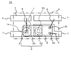
【解決手段】相互に電気的に絶縁されている発光素子1及び受光素子2と、発光素子1から受光素子2へと光を伝達する光導波路3とを備える。光導波路3は光反射性無機粒子を含有する封止樹脂4により覆われている。光反射性無機粒子は、例えば、酸化チタンからなる。発光素子1と受光素子2は、それぞれ基台(例えば、パッケージ端子7)上に設けられ、光導波路3の外面のうち、発光素子1、受光素子2及び基台の何れにも接していない部分の全体が、封止樹脂4により覆われている。
【選択図】図1
Description
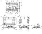
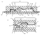
1a 電極
1b PNジャンクション
2 受光素子
2a 電極
2b 受光部
3 光導波路
4 封止樹脂(光反射性無機粒子を含有する樹脂)
5 リードフレーム
6 ボンディングワイヤ
7 パッケージ端子(基台)
10 光結合素子
30 本体部
31 第1接続部
32 第2接続部
41 光透過性樹脂
42 光透過性樹脂
S1 電気信号
S2 光信号
S3 電気信号
Claims (11)
- 相互に電気的に絶縁されている発光素子及び受光素子と、
前記発光素子から前記受光素子へと光を伝達する光導波路と、
前記光導波路の外面の少なくとも一部を覆う、光反射性無機粒子を含有する樹脂と、
を備えることを特徴とする光結合素子。 - 前記光反射性無機粒子は、酸化チタン、酸化アルミ、マイカ(雲母)、窒化アルミ、ボロンナイトライドのうちの少なくとも何れか1種の無機材料の粒子であることを特徴とする請求項1に記載の光結合素子。
- 前記発光素子と前記受光素子は、それぞれ基台上に設けられ、
前記光導波路の外面のうち、前記発光素子、前記受光素子及び前記基台の何れにも接していない部分の全体が、前記光反射性無機粒子を含有する前記樹脂により覆われていることを特徴とする請求項1又は2に記載の光結合素子。 - 前記光導波路は、
平板な板状に形成された本体部と、
前記本体部と前記発光素子とを相互に接続した第1接続部と、
前記本体部と前記受光素子の受光部とを相互に接続した第2接続部と、
からなり、
前記本体部は前記第1及び第2接続部をそれぞれ介して前記発光素子から前記受光素子に亘って架設され、
前記第1接続部は前記発光素子から前記本体部へ、前記本体部は前記第1接続部から前記第2接続部へ、前記第2接続部は前記本体部から前記受光素子へ、順次に光を伝達することを特徴とする請求項1乃至3のいずれか一項に記載の光結合素子。 - 前記発光素子における前記本体部側の面と、前記受光素子における前記本体部側の面とは、前記本体部からの距離が互いに異なり、
前記第1接続部における前記本体部側の面と、前記第2接続部における前記本体部側の面と、が相互に面一となるように、前記第1及び第2接続部の高さがそれぞれ設定されていることを特徴とする請求項4に記載の光結合素子。 - 前記第1接続部と前記第2接続部とは相互に離間し、前記第1接続部と前記第2接続部との間に前記光反射性無機粒子を含有する前記樹脂が介在していることを特徴とする請求項4又は5に記載の光結合素子。
- 前記本体部は光透過性のフィルムであることを特徴とする請求項4乃至6のいずれか一項に記載の光結合素子。
- 相互に電気的に絶縁されている発光素子及び受光素子の前記発光素子から前記受光素子へと光を伝達する光導波路を設ける第1工程と、
前記光導波路を、光反射性無機粒子を含有する樹脂により覆う第2工程と、
をこの順に行うことを特徴とする光結合素子の製造方法。 - 前記第2工程では、
前記光導波路の周囲に型枠を配置する工程と、
前記型枠内に前記光反射性無機粒子を含有する前記樹脂を充填する工程と、
前記充填した樹脂を硬化させる工程と、
をこの順に行うことを特徴とする請求項8に記載の光結合素子の製造方法。 - 前記光導波路は、平板な板状に形成された本体部と、前記本体部と前記発光素子とを相互に接続した第1接続部と、前記本体部と前記受光素子とを相互に接続した第2接続部と、からなり、前記本体部は前記第1及び第2接続部をそれぞれ介して前記発光素子から前記受光素子に亘って架設され、前記第1接続部は前記発光素子から前記本体部へ、前記本体部は前記第1接続部から前記第2接続部へ、前記第2接続部は前記本体部から前記受光素子へ、順次に光を伝達するものであり、
前記発光素子における前記本体部側の面と、前記受光素子における前記本体部側の面とは、前記本体部からの距離が互いに異なり、
前記第1工程では、
前記第1及び第2接続部をそれぞれ構成する光透過性樹脂を、前記第1接続部における前記本体部側の面と、前記第2接続部における前記本体部側の面と、が相互に面一となるように各々の滴下量及び滴下範囲を設定して、前記発光素子及び前記受光素子へそれぞれ滴下する工程と、
前記本体部を、前記第1接続部を構成する前記光透過性樹脂から前記第2接続部を構成する前記光透過性樹脂に亘って架設する工程と、
前記第1接続部を構成する前記光透過性樹脂と前記第2接続部を構成する前記光透過性樹脂とを硬化させる工程と、
をこの順に行うことを特徴とする請求項9に記載の光結合素子の製造方法。 - 光透過性樹脂をそれぞれ前記発光素子及び前記受光素子へ滴下する前記工程では、前記第1接続部と前記第2接続部とが相互に離間し、前記第1接続部と前記第2接続部との間に前記光反射性無機粒子を含有する前記樹脂が介在するように、各々滴下量及び滴下範囲を設定して前記光透過性樹脂を前記発光素子及び前記受光素子へ滴下することを特徴とする請求項10に記載の光結合素子の製造方法。
Priority Applications (3)
| Application Number | Priority Date | Filing Date | Title |
|---|---|---|---|
| JP2009002459A JP2010161202A (ja) | 2009-01-08 | 2009-01-08 | 光結合素子及びその製造方法 |
| US12/652,806 US8143637B2 (en) | 2009-01-08 | 2010-01-06 | Optically coupled device with an optical waveguide |
| US13/341,372 US8288183B2 (en) | 2009-01-08 | 2011-12-30 | Method of manufacturing an optically coupled device |
Applications Claiming Priority (1)
| Application Number | Priority Date | Filing Date | Title |
|---|---|---|---|
| JP2009002459A JP2010161202A (ja) | 2009-01-08 | 2009-01-08 | 光結合素子及びその製造方法 |
Publications (1)
| Publication Number | Publication Date |
|---|---|
| JP2010161202A true JP2010161202A (ja) | 2010-07-22 |
Family
ID=42311117
Family Applications (1)
| Application Number | Title | Priority Date | Filing Date |
|---|---|---|---|
| JP2009002459A Pending JP2010161202A (ja) | 2009-01-08 | 2009-01-08 | 光結合素子及びその製造方法 |
Country Status (2)
| Country | Link |
|---|---|
| US (2) | US8143637B2 (ja) |
| JP (1) | JP2010161202A (ja) |
Families Citing this family (13)
| Publication number | Priority date | Publication date | Assignee | Title |
|---|---|---|---|---|
| JP2010161202A (ja) * | 2009-01-08 | 2010-07-22 | Renesas Electronics Corp | 光結合素子及びその製造方法 |
| US9472536B2 (en) * | 2011-10-11 | 2016-10-18 | Kabushiki Kaisha Toshiba | Semiconductor device and method for manufacturing the same |
| JP5649547B2 (ja) * | 2011-10-11 | 2015-01-07 | 株式会社東芝 | 半導体装置の製造方法 |
| US20140119691A1 (en) * | 2012-10-29 | 2014-05-01 | Avago Technologies General Ip (Singapore) Pte. Ltd. | Opto-coupler with light guide |
| DE102013105229A1 (de) * | 2013-05-22 | 2014-11-27 | Osram Opto Semiconductors Gmbh | Optoelektronisches Bauelement und Verfahren zum Herstellen eines optoelektronischen Bauelementes |
| US10622270B2 (en) | 2017-08-31 | 2020-04-14 | Texas Instruments Incorporated | Integrated circuit package with stress directing material |
| US10553573B2 (en) | 2017-09-01 | 2020-02-04 | Texas Instruments Incorporated | Self-assembly of semiconductor die onto a leadframe using magnetic fields |
| US10833648B2 (en) | 2017-10-24 | 2020-11-10 | Texas Instruments Incorporated | Acoustic management in integrated circuit using phononic bandgap structure |
| US10886187B2 (en) | 2017-10-24 | 2021-01-05 | Texas Instruments Incorporated | Thermal management in integrated circuit using phononic bandgap structure |
| US10371891B2 (en) | 2017-10-31 | 2019-08-06 | Texas Instruments Incorporated | Integrated circuit with dielectric waveguide connector using photonic bandgap structure |
| US10444432B2 (en) * | 2017-10-31 | 2019-10-15 | Texas Instruments Incorporated | Galvanic signal path isolation in an encapsulated package using a photonic structure |
| US10557754B2 (en) | 2017-10-31 | 2020-02-11 | Texas Instruments Incorporated | Spectrometry in integrated circuit using a photonic bandgap structure |
| US10497651B2 (en) | 2017-10-31 | 2019-12-03 | Texas Instruments Incorporated | Electromagnetic interference shield within integrated circuit encapsulation using photonic bandgap structure |
Citations (5)
| Publication number | Priority date | Publication date | Assignee | Title |
|---|---|---|---|---|
| US4450461A (en) * | 1981-07-24 | 1984-05-22 | General Electric Company | Low cost high isolation voltage optocoupler with improved light transmissivity |
| JPS61110474A (ja) * | 1984-11-02 | 1986-05-28 | Nec Corp | 半導体光結合装置 |
| JPH06196747A (ja) * | 1992-12-25 | 1994-07-15 | Sharp Corp | 光結合装置 |
| JPH1154789A (ja) * | 1997-07-30 | 1999-02-26 | Sharp Corp | 光結合素子 |
| JP2002076426A (ja) * | 2000-08-28 | 2002-03-15 | Sharp Corp | 光結合半導体装置及びその製造方法 |
Family Cites Families (9)
| Publication number | Priority date | Publication date | Assignee | Title |
|---|---|---|---|---|
| JPH0637352A (ja) | 1992-07-15 | 1994-02-10 | Sharp Corp | 光結合装置および製造方法 |
| CN1077292C (zh) | 1995-05-02 | 2002-01-02 | 摩托罗拉公司 | 利用安放在封装里的光电发送器和接收器的全息光隔离器 |
| US5751009A (en) * | 1996-04-25 | 1998-05-12 | Motorola, Inc. | Optical isolator having leadframe with non-planar mounting portions |
| JP3731848B2 (ja) | 1998-07-24 | 2006-01-05 | シャープ株式会社 | 光結合装置 |
| US7748912B2 (en) * | 2002-10-29 | 2010-07-06 | Avago Technologies Ecbu Ip (Singapore) Pte. Ltd. | Double mold optocouplers |
| US7021839B2 (en) * | 2002-10-29 | 2006-04-04 | Dominique Ho | Low profile optocouplers |
| TW200414572A (en) * | 2002-11-07 | 2004-08-01 | Matsushita Electric Industrial Co Ltd | LED lamp |
| US7847301B2 (en) * | 2004-12-08 | 2010-12-07 | Agilent Technologies, Inc. | Electronic microcircuit having internal light enhancement |
| JP2010161202A (ja) * | 2009-01-08 | 2010-07-22 | Renesas Electronics Corp | 光結合素子及びその製造方法 |
-
2009
- 2009-01-08 JP JP2009002459A patent/JP2010161202A/ja active Pending
-
2010
- 2010-01-06 US US12/652,806 patent/US8143637B2/en not_active Expired - Fee Related
-
2011
- 2011-12-30 US US13/341,372 patent/US8288183B2/en not_active Expired - Fee Related
Patent Citations (5)
| Publication number | Priority date | Publication date | Assignee | Title |
|---|---|---|---|---|
| US4450461A (en) * | 1981-07-24 | 1984-05-22 | General Electric Company | Low cost high isolation voltage optocoupler with improved light transmissivity |
| JPS61110474A (ja) * | 1984-11-02 | 1986-05-28 | Nec Corp | 半導体光結合装置 |
| JPH06196747A (ja) * | 1992-12-25 | 1994-07-15 | Sharp Corp | 光結合装置 |
| JPH1154789A (ja) * | 1997-07-30 | 1999-02-26 | Sharp Corp | 光結合素子 |
| JP2002076426A (ja) * | 2000-08-28 | 2002-03-15 | Sharp Corp | 光結合半導体装置及びその製造方法 |
Also Published As
| Publication number | Publication date |
|---|---|
| US20100171127A1 (en) | 2010-07-08 |
| US8143637B2 (en) | 2012-03-27 |
| US20120104636A1 (en) | 2012-05-03 |
| US8288183B2 (en) | 2012-10-16 |
Similar Documents
| Publication | Publication Date | Title |
|---|---|---|
| JP2010161202A (ja) | 光結合素子及びその製造方法 | |
| US7943951B2 (en) | Light emitting device package | |
| US20200403107A1 (en) | Light emitting structure | |
| EP0889533B1 (en) | Optical semiconductor module and method for manufacturing same | |
| CN102640369B (zh) | 光通信模块 | |
| EP2654093B1 (en) | Package and method for manufacturing package | |
| KR20130054430A (ko) | 광전 소자 및 그 제조 방법 | |
| CN101425555B (zh) | 半导体发光器件和平面光源 | |
| KR20120032899A (ko) | Led 패키지 및 그 제조방법 | |
| US20100213484A1 (en) | Lead frame assembly, package structure and LED package structure | |
| JP2013098381A (ja) | 光結合素子 | |
| CN103843164A (zh) | 光电半导体组件 | |
| CN214254398U (zh) | 芯片封装结构、感测组件及电子装置 | |
| JP5286122B2 (ja) | 半導体発光装置および半導体発光装置の製造方法 | |
| TWI246612B (en) | Structure having embedded optical electronic components | |
| US8258698B2 (en) | Light emitting device having a molded body with a specific barycenter | |
| JP2010171116A (ja) | 発光装置及び表示装置 | |
| WO2017054696A1 (en) | Semiconductor structure | |
| JP2013251410A (ja) | 光結合素子 | |
| JP6205001B2 (ja) | 光電変換モジュール、及び、アクティブ光ケーブル | |
| CN116130476A (zh) | 一种平面光耦隔离封装结构及其封装工艺 | |
| JP2013065717A (ja) | 半導体装置およびその製造方法 | |
| JP2013179226A (ja) | 光結合装置 | |
| WO2009081980A1 (ja) | 発光装置 | |
| CN213424974U (zh) | 一种光耦合器 |
Legal Events
| Date | Code | Title | Description |
|---|---|---|---|
| A621 | Written request for application examination |
Free format text: JAPANESE INTERMEDIATE CODE: A621 Effective date: 20111024 |
|
| A977 | Report on retrieval |
Free format text: JAPANESE INTERMEDIATE CODE: A971007 Effective date: 20130227 |
|
| A131 | Notification of reasons for refusal |
Free format text: JAPANESE INTERMEDIATE CODE: A131 Effective date: 20130305 |
|
| A521 | Request for written amendment filed |
Free format text: JAPANESE INTERMEDIATE CODE: A523 Effective date: 20130430 |
|
| A131 | Notification of reasons for refusal |
Free format text: JAPANESE INTERMEDIATE CODE: A131 Effective date: 20130806 |
|
| A02 | Decision of refusal |
Free format text: JAPANESE INTERMEDIATE CODE: A02 Effective date: 20131203 |