JP2010272902A - Pulse power supply - Google Patents
Pulse power supply Download PDFInfo
- Publication number
- JP2010272902A JP2010272902A JP2009120484A JP2009120484A JP2010272902A JP 2010272902 A JP2010272902 A JP 2010272902A JP 2009120484 A JP2009120484 A JP 2009120484A JP 2009120484 A JP2009120484 A JP 2009120484A JP 2010272902 A JP2010272902 A JP 2010272902A
- Authority
- JP
- Japan
- Prior art keywords
- pulse
- current
- power supply
- circuit
- capacitor
- Prior art date
- Legal status (The legal status is an assumption and is not a legal conclusion. Google has not performed a legal analysis and makes no representation as to the accuracy of the status listed.)
- Granted
Links
- 239000003990 capacitor Substances 0.000 claims abstract description 66
- 239000004065 semiconductor Substances 0.000 claims abstract description 24
- 230000006835 compression Effects 0.000 claims abstract description 22
- 238000007906 compression Methods 0.000 claims abstract description 22
- 238000007599 discharging Methods 0.000 claims description 4
- 230000002265 prevention Effects 0.000 abstract description 10
- 230000000903 blocking effect Effects 0.000 abstract description 7
- 230000005415 magnetization Effects 0.000 description 18
- 229920006395 saturated elastomer Polymers 0.000 description 13
- 238000010586 diagram Methods 0.000 description 10
- OKTJSMMVPCPJKN-UHFFFAOYSA-N Carbon Chemical compound [C] OKTJSMMVPCPJKN-UHFFFAOYSA-N 0.000 description 5
- 101100439295 Citrus limon ClPT1 gene Proteins 0.000 description 4
- 238000004519 manufacturing process Methods 0.000 description 4
- 230000001172 regenerating effect Effects 0.000 description 4
- 238000004544 sputter deposition Methods 0.000 description 4
- 238000004804 winding Methods 0.000 description 4
- 229910052799 carbon Inorganic materials 0.000 description 3
- 230000015556 catabolic process Effects 0.000 description 3
- 238000000034 method Methods 0.000 description 3
- 238000006731 degradation reaction Methods 0.000 description 2
- 229910003460 diamond Inorganic materials 0.000 description 2
- 239000010432 diamond Substances 0.000 description 2
- 229910002804 graphite Inorganic materials 0.000 description 2
- 239000010439 graphite Substances 0.000 description 2
- 150000002500 ions Chemical class 0.000 description 2
- 238000001755 magnetron sputter deposition Methods 0.000 description 2
- VNWKTOKETHGBQD-UHFFFAOYSA-N methane Chemical compound C VNWKTOKETHGBQD-UHFFFAOYSA-N 0.000 description 2
- 238000007634 remodeling Methods 0.000 description 2
- 239000000758 substrate Substances 0.000 description 2
- -1 PT1b Proteins 0.000 description 1
- 238000009825 accumulation Methods 0.000 description 1
- 229910003481 amorphous carbon Inorganic materials 0.000 description 1
- 230000015572 biosynthetic process Effects 0.000 description 1
- 125000004432 carbon atom Chemical group C* 0.000 description 1
- 238000005520 cutting process Methods 0.000 description 1
- 230000000694 effects Effects 0.000 description 1
- 230000005684 electric field Effects 0.000 description 1
- 238000001704 evaporation Methods 0.000 description 1
- 238000009413 insulation Methods 0.000 description 1
- 230000002452 interceptive effect Effects 0.000 description 1
- 238000005468 ion implantation Methods 0.000 description 1
- 238000007733 ion plating Methods 0.000 description 1
- 238000010884 ion-beam technique Methods 0.000 description 1
- 239000002245 particle Substances 0.000 description 1
- 238000002360 preparation method Methods 0.000 description 1
- 238000005546 reactive sputtering Methods 0.000 description 1
- 230000008929 regeneration Effects 0.000 description 1
- 238000011069 regeneration method Methods 0.000 description 1
- 239000011343 solid material Substances 0.000 description 1
Images


Landscapes
- Plasma Technology (AREA)
Abstract
Description
本発明は、半導体素子をパルス発生スイッチとするパルス発生回路と、パルス電流で充電されるコンデンサを可飽和リアクトルの磁気スイッチ動作により磁気パルス圧縮したパルス電流を得る磁気パルス圧縮回路とを組み合わせたパルス電源に関し、特にプラズマ応用装置などの低インピーダンスとなる負荷放電管に双極性の高電圧パルスを印加するパルス電源に関する。 The present invention is a pulse that combines a pulse generation circuit that uses a semiconductor element as a pulse generation switch and a magnetic pulse compression circuit that obtains a pulse current obtained by compressing a capacitor charged with a pulse current by a magnetic switch operation of a saturable reactor. More particularly, the present invention relates to a pulse power source that applies a bipolar high voltage pulse to a load discharge tube having a low impedance such as a plasma application apparatus.
半導体素子をパルス発生スイッチとするパルス電源としては、図5に例を示すエキシマレーザ用パルス電源がある(特許文献1参照)。図中、パルス発生回路1は、電力用の初段コンデンサC0を充電器2により初期充電しておき、半導体スイッチIGBT1のオン制御で初段コンデンサC0から可飽和リアクトルSI0を通してパルストランスPTにパルス電流を供給する。可飽和リアクトルSI0は、半導体スイッチIGBT1のオンに遅れて磁気スイッチ動作することで半導体スイッチIGBT1のスイッチング損失を軽減するための磁気アシストである。
As a pulse power source using a semiconductor element as a pulse generating switch, there is an excimer laser pulse power source as shown in FIG. 5 (see Patent Document 1). In the figure, a
磁気パルス圧縮回路3は、パルストランスPTで昇圧したパルス電流でコンデンサC1を高圧充電し、このコンデンサC1の充電電圧で可飽和リアクトルSI1が磁気スイッチ動作することによりコンデンサC1からコンデンサC2への狭幅のパルス電流を発生させてコンデンサC2を高圧充電し、さらにコンデンサC2の充電電圧で可飽和リアクトルSI2が磁気スイッチ動作することによりコンデンサC2からエキシマレーザヘッドになる負荷装置4に狭幅・高電圧のパルス電流を供給する。
Magnetic
可飽和リアクトルSI0〜SI2は、磁気スイッチ動作に備えて磁気飽和方向を初期化するための磁化リセットがなされる。この磁化リセットには、各可飽和リアクトルSI0〜SI2にはリセット巻線を設け、直流電流を供給する。 Saturable reactors SI0-SI2 are subjected to magnetization reset for initializing the magnetic saturation direction in preparation for the magnetic switch operation. For this magnetization reset, a reset winding is provided in each of the saturable reactors SI0 to SI2, and a direct current is supplied.
ここで、負荷4は、エキシマレーザ用とする場合、その等価回路は図6の(a)に示すように、ピーキングコンデンサCpに配線インダクタンスLpと負荷放電管の放電抵抗RLが直列に接続された回路になっており、図6の(b)に示すような振動波形となる低インピーダンス負荷(数Ω)となっている。そのため、負荷4で吸収されなかったエネルギーは反転して磁気パルス圧縮回路3を経てパルス発生回路1側に戻ってくる(キックバックエネルギーと呼ばれる)。この電源に戻ってきたキックバックエネルギーは、パルストランスPTの巻線N1’を介して取り込み、ダイオードD1を通してコンデンサC0に初期充電と同じ極性で充電し、次回のパルス発生時の電気エネルギーとして回生する。また、このときIGBT1はオフしており、PTの巻線N1には電流は流れない。
Here, when the
図7は特許文献2に記載されるパルス電源の構成例を示す。同図は、パルスエネルギーの増大を図りながら回路部品責務を下げ、さらにパルス発生の繰り返し周波数を高めるために、2並列のパルス発生回路1a,1bを設け、これらパルス発生回路を時分割運転し、磁気パルス圧縮回路3a,3bは各パルス電流出力をそれぞれ入力して各パルス電流を磁気パルス圧縮する。また、磁気パルス圧縮回路3a,3bは、可飽和リアクトルSI2a,SI2bに電流回り込み防止用ダイオードD1a,D1bを直列接続して各出力を並列接続し、最終段の磁気パルス圧縮回路3にパルス電流を供給する。
FIG. 7 shows a configuration example of a pulse power supply described in
上記の図5や図7のようなパルス電源は、単極性の出力となる。これに対し、プラズマ応用装置としてのDLC(Diamond Like Carbon)成膜装置や半導体成膜装置では、以下に詳細に説明するように、双極性のパルス電源が必要となる場合がある。 The pulse power supply as shown in FIGS. 5 and 7 has a unipolar output. On the other hand, a DLC (Diamond Like Carbon) film forming apparatus or a semiconductor film forming apparatus as a plasma application apparatus may require a bipolar pulse power source as will be described in detail below.
DLC膜は、ダイヤモンドのSP3結合とグラファイトのSP2結合の両者を炭素原子の骨格構造としたアモルファス炭素膜であり、高硬度、高耐摩耗性、低摩擦係数、高絶縁性などの特徴を持ち、電気・電子機器や切削工具、金型、自動車部品などに幅広く応用されている。 The DLC film is an amorphous carbon film in which both the SP 3 bond of diamond and the SP 2 bond of graphite have a skeleton structure of carbon atoms, and has features such as high hardness, high wear resistance, low friction coefficient, and high insulation. It is widely applied to electrical and electronic equipment, cutting tools, molds, and automotive parts.
DLCの成膜には、例えば、メタンなどの含炭素気体またはグラファイトなどの固体原料に放電などでエネルギーを与えて炭素を含む正イオンを生成させ、このイオンを電界で加速して陰極基板上に供給することにより、基板上にDLC膜を生成させる。この生成手法として、イオンビーム蒸着法やアークイオンプレーティング法、スパッタリング法がある。同様に、半導体成膜装置ではスパッタリング法やCVD法、イオン注入法で半導体の成膜を得ている。 For film formation of DLC, for example, a carbon-containing gas such as methane or a solid material such as graphite is given energy by discharge or the like to generate positive ions containing carbon, and the ions are accelerated by an electric field to be formed on the cathode substrate. By supplying, a DLC film is formed on the substrate. As the generation method, there are an ion beam evaporation method, an arc ion plating method, and a sputtering method. Similarly, a semiconductor film forming apparatus obtains a semiconductor film by sputtering, CVD, or ion implantation.
図8はバイポーラ型マグネトロンスパッタ装置の概略図を示す(例えば、非特許文献1参照)。このバイポーラ型では、パルス電源から2つのターゲットにACあるいはパルス電圧を印加する方法として、電圧の半周期毎にターゲットをそれぞれカソードとアノードを入れ替える。同図ではマグネトロン電源MPSの高圧直流出力の極性をパルスユニットPUで交互に切り替えることで、2つのターゲットM1、M2に正負のパルス電圧を印加する。このようなパルス電圧印加方法によれば、ターゲットM1、M2の電位が交互に反転し、スパッタリングにおけるアーキングの発生を防ぐことができる。このアーキングは、直流スパッタリングによってカソード表面絶縁層に電荷が蓄積されることが原因とされ、これを防ぐためにターゲットM1、M2の電位を交互に反転させ、両ターゲットM1、M2の表面に形成された絶縁層上の正電荷を中和させ、次の負電圧印加期間に絶縁層を除去する。 FIG. 8 shows a schematic diagram of a bipolar magnetron sputtering apparatus (see, for example, Non-Patent Document 1). In this bipolar type, as a method of applying AC or pulse voltage to two targets from a pulse power supply, the cathode and the anode are switched for each half cycle of the voltage. In the figure, positive and negative pulse voltages are applied to the two targets M1 and M2 by alternately switching the polarity of the high-voltage DC output of the magnetron power source MPS by the pulse unit PU. According to such a pulse voltage application method, the potentials of the targets M1 and M2 are alternately reversed, and the occurrence of arcing in sputtering can be prevented. This arcing is caused by the accumulation of electric charges in the cathode surface insulating layer by direct current sputtering, and in order to prevent this, the potentials of the targets M1 and M2 are alternately reversed and formed on the surfaces of both targets M1 and M2. The positive charge on the insulating layer is neutralized, and the insulating layer is removed in the next negative voltage application period.
図9は、特許文献3に記載されるDLC成膜装置の回路構成である。この装置に使用されるパルス電源は、負の高電圧パルス発生電源PS(N)、正の高電圧パルス発生電源PS(P)及び干渉防止回路IPCで構成される。
FIG. 9 shows a circuit configuration of the DLC film forming apparatus described in
負の高電圧パルス電源PS(N)は真空管スイッチSW1のスイッチ動作により負の高電圧パルスを出力する。正の高電圧パルス電源PS(P)は真空管スイッチSW2のスイッチ動作により正の高電圧パルスを出力する。これら正負パルス出力は干渉防止回路IPCを通してチャンバCH内の成膜処理物TGに交互に印加される。干渉防止回路IPCは、サージ電流をコアCOREと抵抗R1で限流し、さらにパルスのスイッチング時の過度電流をインダクタンスLで限流し、ダイオードDと抵抗R2を介して回生し、干渉を防止している。 The negative high voltage pulse power supply PS (N) outputs a negative high voltage pulse by the switching operation of the vacuum tube switch SW1. The positive high voltage pulse power supply PS (P) outputs a positive high voltage pulse by the switching operation of the vacuum tube switch SW2. These positive and negative pulse outputs are alternately applied to the film-formed processed product TG in the chamber CH through the interference prevention circuit IPC. The interference prevention circuit IPC limits the surge current by the core CORE and the resistor R1, and further limits the excessive current at the time of pulse switching by the inductance L, and regenerates it through the diode D and the resistor R2, thereby preventing interference. .
前記のように、プラズマ応用装置(DLC成膜装置や半導体成膜装置)に使用されるパルス電源は、パルス発生のスイッチ手段としてサイラトロンや真空管などのギャップスイッチが用いられていたが、他のスイッチ手段として半導体スイッチや磁気スイッチも用いられており、これらの特徴は下記表に示すようになる。 As described above, the pulse power source used in the plasma application apparatus (DLC film forming apparatus or semiconductor film forming apparatus) uses a gap switch such as a thyratron or a vacuum tube as a pulse generating switch means. As a means, a semiconductor switch or a magnetic switch is also used, and these features are as shown in the following table.

これら特徴から、プラズマ応用装置用のパルス電源として、寿命や安定性、制御性などに優れる半導体スイッチおよび磁気スイッチを併用したパルス電源が好適となる。 From these characteristics, a pulse power source that uses a semiconductor switch and a magnetic switch that are excellent in lifetime, stability, controllability, and the like is suitable as a pulse power source for plasma application apparatuses.
しかし、前記の図5や図7に示す半導体スイッチを用いたパルス電源は、単極性のパルス出力になり、双極性のパルスを発生できるものが要求される。すなわち、プラズマ応用装置では、前記の反応性スパッタリングにおいて、絶縁層表面に蓄積した正電荷により局所的な絶縁破壊の発生(アーキングの発生)の問題があり、このアーキングにより発生したパーティクルによって膜質の劣化や電源へのダメージといった問題を引き起こす。このアーキング防止のためには双極性のパルスを発生できるパルス電源が要求される。 However, the pulse power source using the semiconductor switch shown in FIGS. 5 and 7 is required to have a unipolar pulse output and generate a bipolar pulse. That is, in the plasma application apparatus, there is a problem of local breakdown (occurrence of arcing) due to the positive charges accumulated on the surface of the insulating layer in the reactive sputtering, and the film quality is deteriorated by the particles generated by the arcing. Cause problems such as damage to the power supply. In order to prevent this arcing, a pulse power source capable of generating bipolar pulses is required.
双極性のパルスを発生できるパルス電源として、図9に示すように、それぞれが単極性のパルス発生電源になる2台の高電圧パルス発生電源PS(P)、PS(N)を併設し、これらパルス電源から交互にパルスを発生させることが考えられるが、これには正負パルス出力が互いに干渉するのを防止するための干渉防止回路IPC(図9参照)や電流阻止回路(図7のダイオードD1aやD1b)などが必要となる。これら干渉防止回路や電流阻止回路に使用するダイオードや抵抗、リアクトルとしては、耐電圧・電流容量が大きく、従い大型で高価なものになる。また、真空管スイッチを用いることで、安定性が低い、短寿命の問題もある。 As shown in FIG. 9, two high-voltage pulse generation power supplies PS (P) and PS (N) each serving as a unipolar pulse generation power supply are provided as pulse power supplies capable of generating bipolar pulses. It is conceivable to generate pulses alternately from the pulse power supply. This includes an interference prevention circuit IPC (see FIG. 9) and a current blocking circuit (diode D1a in FIG. 7) for preventing the positive and negative pulse outputs from interfering with each other. And D1b) are required. The diodes, resistors, and reactors used in these interference prevention circuits and current blocking circuits have a large withstand voltage and current capacity, and are therefore large and expensive. In addition, the use of a vacuum tube switch has a problem of low stability and short life.
本発明の目的は、半導体素子および磁気スイッチをスイッチ手段として負荷放電管に安定した双極性のパルスを印加でき、しかも干渉防止回路や電流阻止回路を不要にすると共にキックバックエネルギーの回生ができるパルス電源を提供することにある。 It is an object of the present invention to apply a stable bipolar pulse to a load discharge tube using a semiconductor element and a magnetic switch as a switching means, and eliminates the need for an interference prevention circuit and a current blocking circuit and at the same time regenerates kickback energy. To provide power.
本発明は、前記の課題を解決するため、パルス発生回路と磁気パルス圧縮回路で構成する2台のパルス電源を使用し、両パルス電源の出力電圧の極性を逆にした構成とし、両パルス発生回路の時分割運転でそれぞれパルス電流を発生し、負荷に双極性のパルス電流を出力するようにしたもので、以下の構成を特徴とする。 In order to solve the above-mentioned problems, the present invention uses two pulse power sources composed of a pulse generation circuit and a magnetic pulse compression circuit, and has a configuration in which the polarities of the output voltages of both pulse power sources are reversed to generate both pulses. Each circuit generates pulse currents in a time-sharing operation and outputs bipolar pulse currents to the load. The circuit has the following configuration.
(1)予備充電される初段コンデンサから半導体スイッチによる放電でパルス電流を発生するパルス発生回路と、前記パルス電流で充電されるコンデンサを可飽和リアクトルの磁気スイッチ動作により磁気パルス圧縮したパルス電流を得る磁気パルス圧縮回路とを組み合わせたパルス電源において、
前記パルス発生回路および前記磁気パルス圧縮回路は2台構成で、それぞれ出力電圧の極性を逆にした構成とし、各パルス発生回路の時分割運転でそれぞれパルス電流を発生し、負荷に双極性のパルス電流を出力することを特徴とするパルス電源。
(1) A pulse generation circuit that generates a pulse current by discharging with a semiconductor switch from a first-stage capacitor that is precharged, and a pulse current obtained by compressing a magnetic pulse of the capacitor charged by the pulse current by a magnetic switch operation of a saturable reactor is obtained. In a pulse power supply combined with a magnetic pulse compression circuit,
The pulse generation circuit and the magnetic pulse compression circuit are composed of two units, each having a configuration in which the polarity of the output voltage is reversed, each pulse generation circuit generates a pulse current in a time-sharing operation, and a bipolar pulse is applied to the load. A pulse power supply characterized by outputting current.
(2)予備充電される初段コンデンサから半導体スイッチによる放電でパルス電流を発生するパルス発生回路と、前記パルス電流で充電されるコンデンサを可飽和リアクトルの磁気スイッチ動作により磁気パルス圧縮したパルス電流を得る磁気パルス圧縮回路とを組み合わせたパルス電源において、
前記パルス発生回路および前記磁気パルス圧縮回路は2台構成で、片方の出力回路にパルストランスを接続してそれぞれ出力電圧の極性を逆にした構成とし、各パルス発生回路の時分割運転でそれぞれパルス電流を発生し、負荷に双極性のパルス電流を出力することを特徴とするパルス電源。
(2) A pulse generation circuit that generates a pulse current by discharging with a semiconductor switch from a first-stage capacitor that is precharged, and a pulse current obtained by compressing the capacitor charged by the pulse current by a magnetic switch operation of a saturable reactor are obtained. In a pulse power supply combined with a magnetic pulse compression circuit,
The pulse generation circuit and the magnetic pulse compression circuit are configured in two units, with a configuration in which a pulse transformer is connected to one output circuit and the polarity of each output voltage is reversed, and each pulse generation circuit performs a pulse-sharing operation in a time-sharing operation. A pulse power supply that generates current and outputs bipolar pulse current to the load.
以上のとおり、本発明によれば、パルス発生回路と磁気パルス圧縮回路で構成する2台のパルス電源を使用し、両パルス電源の出力電圧の極性を逆にした構成とし、両パルス発生回路の時分割運転でそれぞれパルス電流を発生し、負荷に双極性のパルス電流を出力するようにしたため、半導体素子および磁気スイッチをスイッチ手段として負荷放電管に安定した双極性のパルスを印加でき、しかも干渉防止回路や電流阻止回路を不要にすると共にキックバックエネルギーの回生ができる
具体的には、
・プラズマ応用装置の負荷放電電極に、双極性のパルスを印加できる。
As described above, according to the present invention, two pulse power supplies configured by a pulse generation circuit and a magnetic pulse compression circuit are used, and the polarity of the output voltage of both pulse power supplies is reversed. Since each pulse current is generated by time-sharing operation and bipolar pulse current is output to the load, a stable bipolar pulse can be applied to the load discharge tube using the semiconductor element and magnetic switch as a switching means, and interference Specifically, the prevention circuit and current blocking circuit are not required and kickback energy can be regenerated.
-Bipolar pulses can be applied to the load discharge electrode of plasma application equipment.
・プラズマ応用装置の負荷放電電極で、アーキングの発生をなくし、膜質の劣化や電源へのダメージといった問題が解決する。 ・ Eliminates arcing in the load discharge electrode of plasma application equipment, solving problems such as film quality degradation and power supply damage.
・パルス電源間の干渉防止回路や電流阻止回路が不要になる。 ・ No need for interference prevention circuit or current blocking circuit between pulse power supplies.
・負荷で吸収されない余剰エネルギーが初段コンデンサC0に回生できる。 • Surplus energy that is not absorbed by the load can be regenerated in the first stage capacitor C0.
・パルス電源が半導体スイッチと磁気圧縮回路で構成されるため、高電圧・大電流の急峻なパルスを高繰り返しで安定供給できる。 ・ Since the pulse power supply is composed of a semiconductor switch and a magnetic compression circuit, a steep pulse of high voltage and large current can be stably supplied with high repetition.
・1つのパルス電源とそのパルス電源のパルストランス以降の極性を逆にしたパルス電源の2台で構成できるため、パルス電源の製作が容易である(パルス電源内部の改造のみで対応できる)。 -Since it can be composed of two pulse power supplies, one pulse power supply and a pulse power supply with the polarity after the pulse transformer of the pulse power supply reversed, it is easy to manufacture the pulse power supply (it can be handled only by remodeling inside the pulse power supply).
・1種類のパルス電源を2台使って構成できるため、パルス電源の製作が容易である(パルス電源外部の改造のみで対応できる)。 -Since one type of pulse power supply can be used, it is easy to manufacture the pulse power supply.
・片方のパルス電源の出力部にパルストランスを入れることにより、出力電圧を容易に変化させることができる。 -The output voltage can be easily changed by inserting a pulse transformer in the output section of one pulse power supply.
(実施形態1)
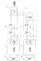
図1は、本実施形態を示すパルス電源の構成図であり、プラズマ応用装置などの低インピーダンスとなる負荷放電管に双極性の高電圧パルスを印加できるパルス電源としている。
(Embodiment 1)
FIG. 1 is a configuration diagram of a pulse power source according to the present embodiment, which is a pulse power source capable of applying a bipolar high voltage pulse to a load discharge tube having a low impedance such as a plasma application apparatus.
同図において、パルス発生回路11a,11bと充電器12a,12bおよび磁気パルス圧縮回路13a,13bは2台構成で、それぞれ出力パルス電圧の極性が逆になる回路構成とし、各パルス発生回路11a,11bの交互運転でそれぞれパルス電流を発生し、負荷14に双極性のパルス電流を出力する。
In the figure, the
パルス発生回路11a,11bおよび磁気パルス圧縮回路13a,13bの具体的な回路構成は、例えば図5に示すものと同様の構成にされ、キックバックエネルギーの回生機能も備える。ただし、パルス発生回路11a,11bのパルストランスPT1aとPT1bの出力極性は互いに逆にし、磁気パルス圧縮回路13a,13bの可飽和リアクトルSI1a、SI2aとSI1b、SI2bの初期磁化方向(→で示す)も逆にする。なお、ピーキングコンデンサCpは負荷14の構成によっては不要のものもあり、この場合は直接に負荷放電管を接続する。
Specific circuit configurations of the
図1の構成によるパルス電源で、負荷(負荷放電電極)14に双極性の高電圧パルスを印加するための動作を図2で説明する。 The operation for applying a bipolar high voltage pulse to the load (load discharge electrode) 14 with the pulse power supply having the configuration of FIG. 1 will be described with reference to FIG.
基本動作は、2台のパルス電源を交互に運転し、負荷放電電極に正負双極性のパルス電圧を印加し、放電を起こす。交互運転のタイミングは、図示していないが制御回路による充電指令とパルス発生回路の半導体スイッチのゲートトリガで任意のタイミングに出力する。なお、交互運転のタイミングは、等間隔でも良いし、正負パルスが近接していても良い。ただし、正パルス発生後、磁化リセット動作中に負パルス発生など近すぎると問題がある。また、各パルス電源の出力電圧も任意に設定できる。すなわち、正負パルスの波高値が多少違っていても良い。 In the basic operation, two pulse power sources are alternately operated, and positive and negative bipolar pulse voltages are applied to the load discharge electrodes to cause discharge. Although not shown, the alternate operation timing is output at an arbitrary timing by a charge command from the control circuit and a gate trigger of the semiconductor switch of the pulse generation circuit. Note that the timing of the alternating operation may be equal intervals, or positive and negative pulses may be close to each other. However, there is a problem if a negative pulse is too close during the magnetization reset operation after the positive pulse is generated. Also, the output voltage of each pulse power supply can be set arbitrarily. That is, the peak values of the positive and negative pulses may be slightly different.
(A)図2の上側のパルス電源の動作
(初期条件)充電器12aでパルス発生回路11a内の初段コンデンサC0(図5参照)を一定電圧まで充電しておく。各可飽和リアクトルSI1a,SI2aを初期磁化状態(図中の矢印の方向)に磁化する。同様に、パルス発生回路11a内の可飽和リアクトルSI0(図5参照)を初期磁化状態に磁化しておく。
(A) Operation of upper pulse power supply in FIG. 2 (Initial condition)
(電流i11および電流i11’)パルス発生回路11aでパルスを発生し、パルストランスPT1aが図示の方向でトランス動作し、コンデンサC1aを負に充電する。
(Current i 11 and current i 11 ′) A pulse is generated by the
(電流i12)可飽和リアクトルSI1aが飽和し、コンデンサC1aからC2aにエネルギー転送される。 (Current i 12 ) Saturable reactor SI1a is saturated and energy is transferred from capacitor C1a to C2a.
(電流i13)可飽和リアクトルSI2aが飽和し、コンデンサC2aからCpにエネルギー転送される。このとき、図2の下側のパルス電源へはほとんど電流が流れない。すなわち、コンデンサCpの電圧により可飽和リアクトルSI2bも磁化しようとするが、可飽和リアクトルSI2bが飽和する時間に達する前にコンデンサCpから負荷放電電極14に放電が起き、可飽和リアクトルSI2bが非飽和状態を維持し、可飽和リアクトルSI2b側への電流をブロックする。結果的に、可飽和リアクトルSI2bは初期磁化方向と逆の方向に少し磁化される。
(Current i 13 ) Saturable reactor SI2a is saturated and energy is transferred from capacitor C2a to Cp. At this time, almost no current flows to the lower pulse power supply in FIG. In other words, the saturable reactor SI2b tries to be magnetized by the voltage of the capacitor Cp, but before the time when the saturable reactor SI2b is saturated, a discharge occurs from the capacitor Cp to the
(電流i14)負荷放電電極14で放電が起こり、コンデンサCpの負の電圧が極性反転して正に充電される。
(Current i 14 ) Discharge occurs at the
(電流i15)コンデンサCpからC2aにエネルギー転送される。このとき、図2の下側のパルス電源へは電流が流れない。すなわち、上記電流i13の一部の微小電流で可飽和リアクトルSI2bが非飽和領域に磁化されており、電流をブロックする。 (Current i 15 ) Energy is transferred from the capacitor Cp to C2a. At this time, no current flows to the lower pulse power supply in FIG. That is, the saturable reactor SI2b is magnetized in the non-saturated region by a small current that is a part of the current i 13 and blocks the current.
(電流i16)コンデンサC2aからC1aにエネルギー転送される。 (Current i 16 ) Energy is transferred from the capacitor C2a to C1a.
(電流i17およびi17’)パルス発生回路11a内の回生回路(図5参照)によりコンデンサC0に初期充電極性で回生される。
(Currents i 17 and i 17 ′) The regenerative circuit (see FIG. 5) in the
(B)図2の下側のパルス電源の動作
(初期条件)充電器12bでパルス発生回路11bの初段コンデンサC0(図5参照)を一定電圧まで充電しておく。各可飽和リアクトルSI1b,SI2bを初期磁化状態(図中の矢印の方向)に磁化する。同様に、パルス発生回路11b内の可飽和リアクトルSI0(図5参照)を初期磁化状態に磁化しておく。
(B) Operation of pulse power source in lower side of FIG. 2 (Initial condition)
(電流i21およびi21’)パルス発生回路11bでパルスを発生し、パルストランスPT1bが図示の方向でトランス動作し、コンデンサC1bを正に充電する。
(Currents i 21 and i 21 ′) A pulse is generated by the
(電流i22)可飽和リアクトルSI1bが飽和し、コンデンサC1bからC2bにエネルギー転送される。 (Current i 22 ) Saturable reactor SI1b is saturated and energy is transferred from capacitor C1b to C2b.
(電流i23)可飽和リアクトルSI2bが飽和し、コンデンサC2bからCpにエネルギー転送される。このとき、図2の上側のパルス電源へはほとんど電流が流れない。すなわち、コンデンサCpの電圧により可飽和リアクトルSI2aも磁化しようとするが、可飽和リアクトルSI2aが飽和する時間に達する前にコンデンサCpから負荷放電電極14に放電が起き、可飽和リアクトルSI2aが非飽和状態を維持し、可飽和リアクトルSI2a側への電流をブロックする。結果的に、可飽和リアクトルSI2aは初期磁化方向と逆の方向に少し磁化される。
(Current i 23 ) Saturable reactor SI2b is saturated and energy is transferred from capacitor C2b to Cp. At this time, almost no current flows to the upper pulse power supply in FIG. In other words, the saturable reactor SI2a tries to be magnetized by the voltage of the capacitor Cp, but before the saturation time of the saturable reactor SI2a is reached, a discharge occurs from the capacitor Cp to the
(電流i24)負荷放電電極14で放電が起こり、コンデンサCpの正の電圧が極性反転して負に充電される。
(Current i 24 ) Discharge occurs at the
(電流i25)コンデンサCpからC2bにエネルギー転送される。このとき、図2の上側のパルス電源へは電流が流れない。すなわち、上記電流i23の一部の微小電流で可飽和リアクトルSI2aが非飽和領域に磁化されており、電流をブロックする。 (Current i 25 ) Energy is transferred from the capacitor Cp to C2b. At this time, no current flows to the upper pulse power supply in FIG. In other words, the saturable reactor SI2a in some small current of the current i 23 are magnetized in the non-saturation region, blocks the current.
(電流i26)コンデンサC2bからC1bにエネルギー転送される。 (Current i 26 ) Energy is transferred from the capacitor C2b to C1b.
(電流i27およびi27’)パルス発生回路11b内の回生回路(図5参照)によりコンデンサC0に初期充電極性で回生される。
(Currents i 27 and i 27 ′) The regenerative circuit (see FIG. 5) in the
したがって、本実施形態によれば、
・プラズマ応用装置の負荷放電電極に、双極性のパルスを印加できる。
Therefore, according to this embodiment,
-Bipolar pulses can be applied to the load discharge electrode of plasma application equipment.
・プラズマ応用装置の負荷放電電極で、アーキングの発生をなくし、膜質の劣化や電源へのダメージといった問題が解決する。 ・ Eliminates arcing in the load discharge electrode of plasma application equipment, solving problems such as film quality degradation and power supply damage.
・パルス電源間の干渉防止回路や電流阻止回路が不要になる。 ・ No need for interference prevention circuit or current blocking circuit between pulse power supplies.
・負荷で吸収されない余剰エネルギーが初段コンデンサC0に回生できる。 • Surplus energy that is not absorbed by the load can be regenerated in the first stage capacitor C0.
・パルス電源が半導体スイッチと磁気圧縮回路で構成されるため、高電圧・大電流の急峻なパルスを高繰り返しで安定供給できる。 ・ Since the pulse power supply is composed of a semiconductor switch and a magnetic compression circuit, a steep pulse of high voltage and large current can be stably supplied with high repetition.
・1つのパルス電源とそのパルス電源のパルストランス以降の極性を逆にしたパルス電源の2台で構成できるため、パルス電源の製作が容易である(パルス電源内部の改造のみで対応できる)。 -Since it can be composed of two pulse power supplies, one pulse power supply and a pulse power supply with the polarity after the pulse transformer of the pulse power supply reversed, it is easy to manufacture the pulse power supply (it can be handled only by remodeling inside the pulse power supply).
(実施形態2)
図3は、本実施形態を示すパルス電源の構成図であり、図1と異なる部分は2台のパルス電源のうち、片方のパルス電源は出力をそのままコンデンサCpに接続し、もう片方のパルス電源は出力にパルストランス回路16を介してコンデンサCpに接続した構成とする。
(Embodiment 2)
FIG. 3 is a block diagram of the pulse power supply according to the present embodiment. The difference from FIG. 1 is that one of the two pulse power supplies has the output connected to the capacitor Cp as it is, and the other pulse power supply. Is configured such that the output is connected to the capacitor Cp via the
2台のパルス電源の極性はどちらでも良い。ここでは2台とも負極性出力とする(同じ電源回路構成)。パルストランス回路16のPT2は、パルストランスがない電源の極性と逆の極性で出力する巻線構成とする。コンデンサCpは負荷14の構成によっては不要のものもあり、この場合は直接に負荷放電管を接続する。
The polarity of the two pulse power supplies may be either. Here, both units have negative output (same power supply circuit configuration). The PT2 of the
図3の構成によるパルス電源で、負荷(負荷放電電極)14に双極性の高電圧パルスを印加するための動作を図4で説明する。 The operation for applying a bipolar high voltage pulse to the load (load discharge electrode) 14 with the pulse power supply having the configuration of FIG. 3 will be described with reference to FIG.
基本動作は、2台のパルス電源を交互に運転し、負荷放電電極に正負双極性のパルス電圧を印加し、放電を起こす。交互運転のタイミングは、図示していないが制御回路による充電指令とパルス発生回路の半導体スイッチのゲートトリガで任意のタイミングに出力する。なお、交互運転のタイミングは等間隔でも良いし、正負パルスが近接していても良い。ただし、正パルス発生後、磁化リセット動作中に負パルス発生など近すぎると問題がある。また、各パルス電源の出力電圧も任意に設定できる。すなわち、正負パルスの波高値が多少違っていても良い。 In the basic operation, two pulse power sources are alternately operated, and positive and negative bipolar pulse voltages are applied to the load discharge electrodes to cause discharge. Although not shown, the alternate operation timing is output at an arbitrary timing by a charge command from the control circuit and a gate trigger of the semiconductor switch of the pulse generation circuit. Note that the timing of the alternating operation may be equal, or the positive and negative pulses may be close. However, there is a problem if a negative pulse is too close during the magnetization reset operation after the positive pulse is generated. Also, the output voltage of each pulse power supply can be set arbitrarily. That is, the peak values of the positive and negative pulses may be slightly different.
(A)図4の上側のパルス電源の動作
(初期条件)充電器12aでパルス発生回路11a内の初段コンデンサC0(図5参照)を一定電圧まで充電しておく。各可飽和リアクトルSI1a,SI2aを初期磁化状態(図中の矢印の方向)に磁化する。同様に、パルス発生回路11a内の可飽和リアクトルSI0(図5参照)を初期磁化状態に磁化しておく。
(A) Operation of upper pulse power supply in FIG. 4 (Initial condition)
(電流i11およびi11’)パルス発生回路11aでパルスを発生し、パルストランスPT1aが図示の方向でトランス動作し、コンデンサC1aを負に充電する。
(Currents i 11 and i 11 ′) A pulse is generated by the
(電流i12)可飽和リアクトルSI1aが飽和し、コンデンサC1aからC2aにエネルギー転送される。 (Current i 12 ) Saturable reactor SI1a is saturated and energy is transferred from capacitor C1a to C2a.
(電流i13)可飽和リアクトルSI2aが飽和し、コンデンサC2aからCpにエネルギー転送される。このとき、図4の下側のパルス電源へはほとんど電流が流れない。すなわち、可飽和リアクトルSI2bが非飽和で電流をブロックする。このとき、可飽和リアクトルSI2bは初期磁化方向と逆の方向に少し磁化される。 (Current i 13 ) Saturable reactor SI2a is saturated and energy is transferred from capacitor C2a to Cp. At this time, almost no current flows to the lower pulse power supply in FIG. That is, the saturable reactor SI2b is not saturated and blocks current. At this time, the saturable reactor SI2b is slightly magnetized in the direction opposite to the initial magnetization direction.
(電流i14)負荷放電電極14で放電が起こり、コンデンサCpの負の電圧が極性反転して正に充電される。
(Current i 14 ) Discharge occurs at the
(電流i15)コンデンサCpからC2aにエネルギー転送される。このとき、図4の下側のパルス電源へは電流が流れない。すなわち、上記電流i13の一部の微小電流で可飽和リアクトルSI2bが非飽和領域に磁化されており、電流をブロックする。 (Current i 15 ) Energy is transferred from the capacitor Cp to C2a. At this time, no current flows to the lower pulse power supply in FIG. That is, the saturable reactor SI2b is magnetized in the non-saturated region by a small current that is a part of the current i 13 and blocks the current.
(電流i16)コンデンサC2aからC1aにエネルギー転送される。 (Current i 16 ) Energy is transferred from the capacitor C2a to C1a.
(電流i17およびi17’)パルス発生回路11a内の回生回路(図5参照)によりコンデンサC0に初期充電極性で回生される。
(Currents i 17 and i 17 ′) The regenerative circuit (see FIG. 5) in the
(B)図4の下側のパルス電源の動作
(初期条件)充電器12bでパルス発生回路11bの初段コンデンサC0(図5参照)を一定電圧まで充電しておく。各可飽和リアクトルSI1b,SI2bを初期磁化状態(図中の矢印の方向)に磁化する。同様に、パルス発生回路11b内の可飽和リアクトルSI0(図5参照)を初期磁化状態に磁化しておく。
(B) Operation of lower pulse power supply in FIG. 4 (Initial condition)
(電流i21およびi21’)パルス発生回路11bでパルス発生し、パルストランスPT1bが図示の方向でトランス動作し、コンデンサC1bを負に充電する。
(Currents i 21 and i 21 ′) The pulse is generated by the
(電流i22)可飽和リアクトルSI1bが飽和し、コンデンサC1bからC2bにエネルギー転送される。 (Current i 22 ) Saturable reactor SI1b is saturated and energy is transferred from capacitor C1b to C2b.
(電流i23)可飽和リアクトルSI2bが飽和し、コンデンサC2bからCpにエネルギー転送される。このとき、パルストランスPT2がトランス動作する。このとき、図4の上側のパルス電源へはほとんど電流が流れない。すなわち、可飽和リアクトルSI2aが非飽和で電流をブロックする。このとき、可飽和リアクトルSI2aは初期磁化方向と逆の方向に少し磁化される。 (Current i 23 ) Saturable reactor SI2b is saturated and energy is transferred from capacitor C2b to Cp. At this time, the pulse transformer PT2 performs a transformer operation. At this time, almost no current flows to the upper pulse power supply in FIG. That is, the saturable reactor SI2a is not saturated and blocks current. At this time, the saturable reactor SI2a is slightly magnetized in the direction opposite to the initial magnetization direction.
(電流i24)負荷放電電極14で放電が起こり、コンデンサCpの正の電圧が極性反転して負に充電される。
(Current i 24 ) Discharge occurs at the
(電流i25)コンデンサCpからC2bにエネルギー転送される。このとき、パルストランスPT2がトランス動作する。このとき、図4の上側のパルス電源へは電流が流れない。すなわち、上記電流i23の一部の微小電流で可飽和リアクトルSI2aが非飽和領域に磁化されており、電流をブロックする。 (Current i 25 ) Energy is transferred from the capacitor Cp to C2b. At this time, the pulse transformer PT2 performs a transformer operation. At this time, no current flows to the upper pulse power supply in FIG. In other words, the saturable reactor SI2a in some small current of the current i 23 are magnetized in the non-saturation region, blocks the current.
(電流i26)コンデンサC2bからC1bにエネルギー転送される。 (Current i 26 ) Energy is transferred from the capacitor C2b to C1b.
(電流i27およびi27’)パルス発生回路11b内の回生回路(図5参照)によりコンデンサC0に初期充電極性で回生される。
(Currents i 27 and i 27 ′) The regenerative circuit (see FIG. 5) in the
したがって、本実施形態によれば、実施形態1の効果に加えて、
・1種類のパルス電源を2台使って構成できるため、パルス電源の製作が容易である(パルス電源外部の改造のみで対応できる)。
Therefore, according to the present embodiment, in addition to the effects of the first embodiment,
-Since one type of pulse power supply can be used, it is easy to manufacture the pulse power supply.
・片方のパルス電源の出力部にパルストランスを入れることにより、出力電圧を容易に変化させることができる。 -The output voltage can be easily changed by inserting a pulse transformer in the output section of one pulse power supply.
1、11a、11b パルス発生回路
2、12a、12b 充電器
3、13a、13b 磁気パルス圧縮回路
4、14 負荷
5 磁化リセット回路
16 パルストランス回路
PT、PT1a、PT1b、PT2 パルストランス
C0,C1,C2,C1a、C1b、C2a、C2b コンデンサ
Cp ピーキングコンデンサ
SI0,SI1,SI2,SI1a、SI1b、SI2a,SI2b 可飽和リアクトル
DESCRIPTION OF
Claims (2)
前記パルス発生回路および前記磁気パルス圧縮回路は2台構成で、それぞれ出力電圧の極性を逆にした構成とし、各パルス発生回路の時分割運転でそれぞれパルス電流を発生し、負荷に双極性のパルス電流を出力することを特徴とするパルス電源。 A pulse generation circuit that generates a pulse current by discharging a semiconductor switch from a first stage capacitor that is precharged, and a magnetic pulse compression that obtains a pulse current by compressing the capacitor charged by the pulse current by a magnetic switch operation of a saturable reactor In the pulse power supply combined with the circuit,
The pulse generation circuit and the magnetic pulse compression circuit are composed of two units, each having a configuration in which the polarity of the output voltage is reversed, each pulse generation circuit generates a pulse current in a time-sharing operation, and a bipolar pulse is applied to the load. A pulse power supply characterized by outputting current.
前記パルス発生回路および前記磁気パルス圧縮回路は2台構成で、片方の出力回路にパルストランスを接続してそれぞれ出力電圧の極性を逆にした構成とし、各パルス発生回路の時分割運転でそれぞれパルス電流を発生し、負荷に双極性のパルス電流を出力することを特徴とするパルス電源。 A pulse generation circuit that generates a pulse current by discharging a semiconductor switch from a first stage capacitor that is precharged, and a magnetic pulse compression that obtains a pulse current by compressing the capacitor charged by the pulse current by a magnetic switch operation of a saturable reactor In the pulse power supply combined with the circuit,
The pulse generation circuit and the magnetic pulse compression circuit are configured in two units, with a configuration in which a pulse transformer is connected to one output circuit and the polarity of each output voltage is reversed, and each pulse generation circuit performs a pulse-sharing operation in a time-sharing operation. A pulse power supply that generates current and outputs bipolar pulse current to the load.
Priority Applications (1)
| Application Number | Priority Date | Filing Date | Title |
|---|---|---|---|
| JP2009120484A JP5321238B2 (en) | 2009-05-19 | 2009-05-19 | Pulse power supply |
Applications Claiming Priority (1)
| Application Number | Priority Date | Filing Date | Title |
|---|---|---|---|
| JP2009120484A JP5321238B2 (en) | 2009-05-19 | 2009-05-19 | Pulse power supply |
Publications (2)
| Publication Number | Publication Date |
|---|---|
| JP2010272902A true JP2010272902A (en) | 2010-12-02 |
| JP5321238B2 JP5321238B2 (en) | 2013-10-23 |
Family
ID=43420618
Family Applications (1)
| Application Number | Title | Priority Date | Filing Date |
|---|---|---|---|
| JP2009120484A Active JP5321238B2 (en) | 2009-05-19 | 2009-05-19 | Pulse power supply |
Country Status (1)
| Country | Link |
|---|---|
| JP (1) | JP5321238B2 (en) |
Cited By (6)
| Publication number | Priority date | Publication date | Assignee | Title |
|---|---|---|---|---|
| CN103441697A (en) * | 2013-08-20 | 2013-12-11 | 东莞市力与源电器设备有限公司 | Method for controlling positive and negative commutating pulse power supply |
| JPWO2016063678A1 (en) * | 2014-10-20 | 2017-04-27 | 三菱電機株式会社 | Power converter |
| CN113179005A (en) * | 2021-05-25 | 2021-07-27 | 长安大学 | Double-pulse power supply and working method thereof |
| CN113904662A (en) * | 2021-10-20 | 2022-01-07 | 重庆大学 | Pulse generating circuit for outputting bipolar pulse, and method and apparatus thereof |
| CN115021729A (en) * | 2021-03-04 | 2022-09-06 | 北京科益虹源光电技术有限公司 | Magnetic pulse compression method |
| JP2022548206A (en) * | 2019-08-30 | 2022-11-17 | 株式会社ミツトヨ | High-speed, high-power pulsed light source system for high-speed imaging |
Citations (5)
| Publication number | Priority date | Publication date | Assignee | Title |
|---|---|---|---|---|
| JPH02148781A (en) * | 1988-11-29 | 1990-06-07 | Toshiba Corp | Pulse laser power source |
| JP2000124530A (en) * | 1998-10-19 | 2000-04-28 | Meidensha Corp | Pulse power supply device |
| JP2001036173A (en) * | 1999-07-21 | 2001-02-09 | Meidensha Corp | Pulse power source unit |
| JP2007123138A (en) * | 2005-10-31 | 2007-05-17 | Ushio Inc | Extreme ultraviolet light source device |
| JP2007288973A (en) * | 2006-04-19 | 2007-11-01 | Murata Mfg Co Ltd | Positive-negative switching power supply apparatus |
-
2009
- 2009-05-19 JP JP2009120484A patent/JP5321238B2/en active Active
Patent Citations (5)
| Publication number | Priority date | Publication date | Assignee | Title |
|---|---|---|---|---|
| JPH02148781A (en) * | 1988-11-29 | 1990-06-07 | Toshiba Corp | Pulse laser power source |
| JP2000124530A (en) * | 1998-10-19 | 2000-04-28 | Meidensha Corp | Pulse power supply device |
| JP2001036173A (en) * | 1999-07-21 | 2001-02-09 | Meidensha Corp | Pulse power source unit |
| JP2007123138A (en) * | 2005-10-31 | 2007-05-17 | Ushio Inc | Extreme ultraviolet light source device |
| JP2007288973A (en) * | 2006-04-19 | 2007-11-01 | Murata Mfg Co Ltd | Positive-negative switching power supply apparatus |
Non-Patent Citations (1)
| Title |
|---|
| JPN6013013458; 笹本栄二: 'パルス電源応用技術' 明電時報 Vol.323 2009 No.2, 200904, p56-61 * |
Cited By (9)
| Publication number | Priority date | Publication date | Assignee | Title |
|---|---|---|---|---|
| CN103441697A (en) * | 2013-08-20 | 2013-12-11 | 东莞市力与源电器设备有限公司 | Method for controlling positive and negative commutating pulse power supply |
| JPWO2016063678A1 (en) * | 2014-10-20 | 2017-04-27 | 三菱電機株式会社 | Power converter |
| JP2022548206A (en) * | 2019-08-30 | 2022-11-17 | 株式会社ミツトヨ | High-speed, high-power pulsed light source system for high-speed imaging |
| JP7623360B2 (en) | 2019-08-30 | 2025-01-28 | 株式会社ミツトヨ | High-speed, high-power pulsed light source system for high-speed measurement and imaging |
| CN115021729A (en) * | 2021-03-04 | 2022-09-06 | 北京科益虹源光电技术有限公司 | Magnetic pulse compression method |
| CN115021729B (en) * | 2021-03-04 | 2026-04-17 | 北京科益虹源光电技术有限公司 | Magnetic pulse compression method |
| CN113179005A (en) * | 2021-05-25 | 2021-07-27 | 长安大学 | Double-pulse power supply and working method thereof |
| CN113179005B (en) * | 2021-05-25 | 2023-08-01 | 长安大学 | Double-pulse power supply and working method thereof |
| CN113904662A (en) * | 2021-10-20 | 2022-01-07 | 重庆大学 | Pulse generating circuit for outputting bipolar pulse, and method and apparatus thereof |
Also Published As
| Publication number | Publication date |
|---|---|
| JP5321238B2 (en) | 2013-10-23 |
Similar Documents
| Publication | Publication Date | Title |
|---|---|---|
| JP5321238B2 (en) | Pulse power supply | |
| JP5043824B2 (en) | Vacuum plasma generator | |
| JP2013132109A (en) | Impulse voltage generation apparatus | |
| Yan et al. | A triggered spark-gap switch for high-repetition rate high-voltage pulse generation | |
| Scholtz et al. | Asymmetric bipolar plasma power supply to increase the secondary electrons emission in capacitive coupling plasmas | |
| JP6368928B2 (en) | Power supply for DC sputtering equipment | |
| Anders et al. | Efficient, compact power supply for repetitively pulsed,“triggerless” cathodic arcs | |
| Liu et al. | An efficient, repetitive nanosecond pulsed power generator with ten synchronized spark gap switches | |
| Liu et al. | An all solid-state pulsed power generator based on Marx generator | |
| RU2453022C2 (en) | Device for simultaneous power supply to electrophysical instruments with high constant and pulse-frequency voltage of sub-microsecond range (versions) | |
| CN101841253A (en) | Pulsed-liquid phase discharge system based on multiplex IGCT parallel connection | |
| Schneider et al. | The Effect of high-frequency arc conditioning of the electrodes on electric strength of vacuum insulation | |
| US7514819B2 (en) | Semiconductor switch assembly for pulse power apparatus | |
| Tsygankov et al. | Oxide-coated al cathode for decreasing electron leakage and increasing electrical strength of vacuum insulation in the nanosecond pulse range | |
| Kim et al. | Optimal design of− 40-kV long-pulse power supply | |
| US7482786B2 (en) | Electric discharger using semiconductor switch | |
| Balcerak et al. | Topology of a high voltage pulse generator using parasitic parameters of autotransformers for non-thermal plasma generation | |
| Takaki et al. | Ion extraction from magnetically driven carbon shunting arc plasma | |
| Kuzmichev et al. | Integrated Tasitronic Switch for Generating High Voltage | |
| CN102480100A (en) | Pulse discharge device for pulse oxygen-iodine chemical laser | |
| JP2011238575A (en) | Power supply device of surface creepage discharge type ion generating device | |
| RU41951U1 (en) | PULSE ELECTRON ACCELERATOR | |
| Kohno et al. | High-current pulsed power generator ASO-X using inductive voltage adder and inductive energy storage system | |
| JP2005158573A (en) | Plasma generator | |
| Knyaz'Kov et al. | Pulsed welding plasma source |
Legal Events
| Date | Code | Title | Description |
|---|---|---|---|
| A621 | Written request for application examination |
Free format text: JAPANESE INTERMEDIATE CODE: A621 Effective date: 20111209 |
|
| A977 | Report on retrieval |
Free format text: JAPANESE INTERMEDIATE CODE: A971007 Effective date: 20121228 |
|
| A131 | Notification of reasons for refusal |
Free format text: JAPANESE INTERMEDIATE CODE: A131 Effective date: 20130326 |
|
| A521 | Written amendment |
Free format text: JAPANESE INTERMEDIATE CODE: A523 Effective date: 20130522 |
|
| RD02 | Notification of acceptance of power of attorney |
Free format text: JAPANESE INTERMEDIATE CODE: A7422 Effective date: 20130522 |
|
| TRDD | Decision of grant or rejection written | ||
| A01 | Written decision to grant a patent or to grant a registration (utility model) |
Free format text: JAPANESE INTERMEDIATE CODE: A01 Effective date: 20130618 |
|
| A61 | First payment of annual fees (during grant procedure) |
Free format text: JAPANESE INTERMEDIATE CODE: A61 Effective date: 20130701 |
|
| R150 | Certificate of patent or registration of utility model |
Ref document number: 5321238 Country of ref document: JP Free format text: JAPANESE INTERMEDIATE CODE: R150 Free format text: JAPANESE INTERMEDIATE CODE: R150 |