JP2010272902A - パルス電源 - Google Patents
パルス電源 Download PDFInfo
- Publication number
- JP2010272902A JP2010272902A JP2009120484A JP2009120484A JP2010272902A JP 2010272902 A JP2010272902 A JP 2010272902A JP 2009120484 A JP2009120484 A JP 2009120484A JP 2009120484 A JP2009120484 A JP 2009120484A JP 2010272902 A JP2010272902 A JP 2010272902A
- Authority
- JP
- Japan
- Prior art keywords
- pulse
- current
- power supply
- circuit
- capacitor
- Prior art date
- Legal status (The legal status is an assumption and is not a legal conclusion. Google has not performed a legal analysis and makes no representation as to the accuracy of the status listed.)
- Granted
Links
- 239000003990 capacitor Substances 0.000 claims abstract description 66
- 239000004065 semiconductor Substances 0.000 claims abstract description 24
- 230000006835 compression Effects 0.000 claims abstract description 22
- 238000007906 compression Methods 0.000 claims abstract description 22
- 238000007599 discharging Methods 0.000 claims description 4
- 230000002265 prevention Effects 0.000 abstract description 10
- 230000000903 blocking effect Effects 0.000 abstract description 7
- 230000005415 magnetization Effects 0.000 description 18
- 229920006395 saturated elastomer Polymers 0.000 description 13
- 238000010586 diagram Methods 0.000 description 10
- OKTJSMMVPCPJKN-UHFFFAOYSA-N Carbon Chemical compound [C] OKTJSMMVPCPJKN-UHFFFAOYSA-N 0.000 description 5
- 101100439295 Citrus limon ClPT1 gene Proteins 0.000 description 4
- 238000004519 manufacturing process Methods 0.000 description 4
- 230000001172 regenerating effect Effects 0.000 description 4
- 238000004544 sputter deposition Methods 0.000 description 4
- 238000004804 winding Methods 0.000 description 4
- 229910052799 carbon Inorganic materials 0.000 description 3
- 230000015556 catabolic process Effects 0.000 description 3
- 238000000034 method Methods 0.000 description 3
- 238000006731 degradation reaction Methods 0.000 description 2
- 229910003460 diamond Inorganic materials 0.000 description 2
- 239000010432 diamond Substances 0.000 description 2
- 229910002804 graphite Inorganic materials 0.000 description 2
- 239000010439 graphite Substances 0.000 description 2
- 150000002500 ions Chemical class 0.000 description 2
- 238000001755 magnetron sputter deposition Methods 0.000 description 2
- VNWKTOKETHGBQD-UHFFFAOYSA-N methane Chemical compound C VNWKTOKETHGBQD-UHFFFAOYSA-N 0.000 description 2
- 238000007634 remodeling Methods 0.000 description 2
- 239000000758 substrate Substances 0.000 description 2
- -1 PT1b Proteins 0.000 description 1
- 238000009825 accumulation Methods 0.000 description 1
- 229910003481 amorphous carbon Inorganic materials 0.000 description 1
- 230000015572 biosynthetic process Effects 0.000 description 1
- 125000004432 carbon atom Chemical group C* 0.000 description 1
- 238000005520 cutting process Methods 0.000 description 1
- 230000000694 effects Effects 0.000 description 1
- 230000005684 electric field Effects 0.000 description 1
- 238000001704 evaporation Methods 0.000 description 1
- 238000009413 insulation Methods 0.000 description 1
- 230000002452 interceptive effect Effects 0.000 description 1
- 238000005468 ion implantation Methods 0.000 description 1
- 238000007733 ion plating Methods 0.000 description 1
- 238000010884 ion-beam technique Methods 0.000 description 1
- 239000002245 particle Substances 0.000 description 1
- 238000002360 preparation method Methods 0.000 description 1
- 238000005546 reactive sputtering Methods 0.000 description 1
- 230000008929 regeneration Effects 0.000 description 1
- 238000011069 regeneration method Methods 0.000 description 1
- 239000011343 solid material Substances 0.000 description 1
Images


Landscapes
- Plasma Technology (AREA)
Abstract
【解決手段】予備充電される初段コンデンサから半導体スイッチによる放電でパルス電流を発生するパルス発生回路11a、11bと、パルス電流で充電されるコンデンサを可飽和リアクトルの磁気スイッチ動作により磁気パルス圧縮したパルス電流を得る磁気パルス圧縮回路13a、13bとを組み合わせたパルス電源を2台構成とし、それぞれ出力電圧の極性を逆にした構成とし、各パルス発生回路の時分割運転でそれぞれパルス電流を発生し、負荷14に双極性のパルス電流を出力する。
【選択図】図1
Description

前記パルス発生回路および前記磁気パルス圧縮回路は2台構成で、それぞれ出力電圧の極性を逆にした構成とし、各パルス発生回路の時分割運転でそれぞれパルス電流を発生し、負荷に双極性のパルス電流を出力することを特徴とするパルス電源。
前記パルス発生回路および前記磁気パルス圧縮回路は2台構成で、片方の出力回路にパルストランスを接続してそれぞれ出力電圧の極性を逆にした構成とし、各パルス発生回路の時分割運転でそれぞれパルス電流を発生し、負荷に双極性のパルス電流を出力することを特徴とするパルス電源。
具体的には、
・プラズマ応用装置の負荷放電電極に、双極性のパルスを印加できる。
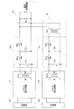
図1は、本実施形態を示すパルス電源の構成図であり、プラズマ応用装置などの低インピーダンスとなる負荷放電管に双極性の高電圧パルスを印加できるパルス電源としている。
(初期条件)充電器12aでパルス発生回路11a内の初段コンデンサC0(図5参照)を一定電圧まで充電しておく。各可飽和リアクトルSI1a,SI2aを初期磁化状態(図中の矢印の方向)に磁化する。同様に、パルス発生回路11a内の可飽和リアクトルSI0(図5参照)を初期磁化状態に磁化しておく。
(初期条件)充電器12bでパルス発生回路11bの初段コンデンサC0(図5参照)を一定電圧まで充電しておく。各可飽和リアクトルSI1b,SI2bを初期磁化状態(図中の矢印の方向)に磁化する。同様に、パルス発生回路11b内の可飽和リアクトルSI0(図5参照)を初期磁化状態に磁化しておく。
・プラズマ応用装置の負荷放電電極に、双極性のパルスを印加できる。
図3は、本実施形態を示すパルス電源の構成図であり、図1と異なる部分は2台のパルス電源のうち、片方のパルス電源は出力をそのままコンデンサCpに接続し、もう片方のパルス電源は出力にパルストランス回路16を介してコンデンサCpに接続した構成とする。
(初期条件)充電器12aでパルス発生回路11a内の初段コンデンサC0(図5参照)を一定電圧まで充電しておく。各可飽和リアクトルSI1a,SI2aを初期磁化状態(図中の矢印の方向)に磁化する。同様に、パルス発生回路11a内の可飽和リアクトルSI0(図5参照)を初期磁化状態に磁化しておく。
(初期条件)充電器12bでパルス発生回路11bの初段コンデンサC0(図5参照)を一定電圧まで充電しておく。各可飽和リアクトルSI1b,SI2bを初期磁化状態(図中の矢印の方向)に磁化する。同様に、パルス発生回路11b内の可飽和リアクトルSI0(図5参照)を初期磁化状態に磁化しておく。
・1種類のパルス電源を2台使って構成できるため、パルス電源の製作が容易である(パルス電源外部の改造のみで対応できる)。
2、12a、12b 充電器
3、13a、13b 磁気パルス圧縮回路
4、14 負荷
5 磁化リセット回路
16 パルストランス回路
PT、PT1a、PT1b、PT2 パルストランス
C0,C1,C2,C1a、C1b、C2a、C2b コンデンサ
Cp ピーキングコンデンサ
SI0,SI1,SI2,SI1a、SI1b、SI2a,SI2b 可飽和リアクトル
Claims (2)
- 予備充電される初段コンデンサから半導体スイッチによる放電でパルス電流を発生するパルス発生回路と、前記パルス電流で充電されるコンデンサを可飽和リアクトルの磁気スイッチ動作により磁気パルス圧縮したパルス電流を得る磁気パルス圧縮回路とを組み合わせたパルス電源において、
前記パルス発生回路および前記磁気パルス圧縮回路は2台構成で、それぞれ出力電圧の極性を逆にした構成とし、各パルス発生回路の時分割運転でそれぞれパルス電流を発生し、負荷に双極性のパルス電流を出力することを特徴とするパルス電源。 - 予備充電される初段コンデンサから半導体スイッチによる放電でパルス電流を発生するパルス発生回路と、前記パルス電流で充電されるコンデンサを可飽和リアクトルの磁気スイッチ動作により磁気パルス圧縮したパルス電流を得る磁気パルス圧縮回路とを組み合わせたパルス電源において、
前記パルス発生回路および前記磁気パルス圧縮回路は2台構成で、片方の出力回路にパルストランスを接続してそれぞれ出力電圧の極性を逆にした構成とし、各パルス発生回路の時分割運転でそれぞれパルス電流を発生し、負荷に双極性のパルス電流を出力することを特徴とするパルス電源。
Priority Applications (1)
| Application Number | Priority Date | Filing Date | Title |
|---|---|---|---|
| JP2009120484A JP5321238B2 (ja) | 2009-05-19 | 2009-05-19 | パルス電源 |
Applications Claiming Priority (1)
| Application Number | Priority Date | Filing Date | Title |
|---|---|---|---|
| JP2009120484A JP5321238B2 (ja) | 2009-05-19 | 2009-05-19 | パルス電源 |
Publications (2)
| Publication Number | Publication Date |
|---|---|
| JP2010272902A true JP2010272902A (ja) | 2010-12-02 |
| JP5321238B2 JP5321238B2 (ja) | 2013-10-23 |
Family
ID=43420618
Family Applications (1)
| Application Number | Title | Priority Date | Filing Date |
|---|---|---|---|
| JP2009120484A Active JP5321238B2 (ja) | 2009-05-19 | 2009-05-19 | パルス電源 |
Country Status (1)
| Country | Link |
|---|---|
| JP (1) | JP5321238B2 (ja) |
Cited By (6)
| Publication number | Priority date | Publication date | Assignee | Title |
|---|---|---|---|---|
| CN103441697A (zh) * | 2013-08-20 | 2013-12-11 | 东莞市力与源电器设备有限公司 | 一种正反换向脉冲电源的控制方法 |
| JPWO2016063678A1 (ja) * | 2014-10-20 | 2017-04-27 | 三菱電機株式会社 | 電力変換装置 |
| CN113179005A (zh) * | 2021-05-25 | 2021-07-27 | 长安大学 | 一种双脉冲电源及其工作方法 |
| CN113904662A (zh) * | 2021-10-20 | 2022-01-07 | 重庆大学 | 用于输出双极性脉冲的脉冲发生电路及其方法、设备 |
| CN115021729A (zh) * | 2021-03-04 | 2022-09-06 | 北京科益虹源光电技术有限公司 | 磁脉冲压缩方法 |
| JP2022548206A (ja) * | 2019-08-30 | 2022-11-17 | 株式会社ミツトヨ | 高速計測撮像のための高速高パワーパルス光源システム |
Citations (5)
| Publication number | Priority date | Publication date | Assignee | Title |
|---|---|---|---|---|
| JPH02148781A (ja) * | 1988-11-29 | 1990-06-07 | Toshiba Corp | パルスレーザ電源装置 |
| JP2000124530A (ja) * | 1998-10-19 | 2000-04-28 | Meidensha Corp | パルス電源装置 |
| JP2001036173A (ja) * | 1999-07-21 | 2001-02-09 | Meidensha Corp | パルス電源装置 |
| JP2007123138A (ja) * | 2005-10-31 | 2007-05-17 | Ushio Inc | 極端紫外光光源装置 |
| JP2007288973A (ja) * | 2006-04-19 | 2007-11-01 | Murata Mfg Co Ltd | 正負切り換え電源装置 |
-
2009
- 2009-05-19 JP JP2009120484A patent/JP5321238B2/ja active Active
Patent Citations (5)
| Publication number | Priority date | Publication date | Assignee | Title |
|---|---|---|---|---|
| JPH02148781A (ja) * | 1988-11-29 | 1990-06-07 | Toshiba Corp | パルスレーザ電源装置 |
| JP2000124530A (ja) * | 1998-10-19 | 2000-04-28 | Meidensha Corp | パルス電源装置 |
| JP2001036173A (ja) * | 1999-07-21 | 2001-02-09 | Meidensha Corp | パルス電源装置 |
| JP2007123138A (ja) * | 2005-10-31 | 2007-05-17 | Ushio Inc | 極端紫外光光源装置 |
| JP2007288973A (ja) * | 2006-04-19 | 2007-11-01 | Murata Mfg Co Ltd | 正負切り換え電源装置 |
Non-Patent Citations (1)
| Title |
|---|
| JPN6013013458; 笹本栄二: 'パルス電源応用技術' 明電時報 Vol.323 2009 No.2, 200904, p56-61 * |
Cited By (9)
| Publication number | Priority date | Publication date | Assignee | Title |
|---|---|---|---|---|
| CN103441697A (zh) * | 2013-08-20 | 2013-12-11 | 东莞市力与源电器设备有限公司 | 一种正反换向脉冲电源的控制方法 |
| JPWO2016063678A1 (ja) * | 2014-10-20 | 2017-04-27 | 三菱電機株式会社 | 電力変換装置 |
| JP2022548206A (ja) * | 2019-08-30 | 2022-11-17 | 株式会社ミツトヨ | 高速計測撮像のための高速高パワーパルス光源システム |
| JP7623360B2 (ja) | 2019-08-30 | 2025-01-28 | 株式会社ミツトヨ | 高速計測撮像のための高速高パワーパルス光源システム |
| CN115021729A (zh) * | 2021-03-04 | 2022-09-06 | 北京科益虹源光电技术有限公司 | 磁脉冲压缩方法 |
| CN115021729B (zh) * | 2021-03-04 | 2026-04-17 | 北京科益虹源光电技术有限公司 | 磁脉冲压缩方法 |
| CN113179005A (zh) * | 2021-05-25 | 2021-07-27 | 长安大学 | 一种双脉冲电源及其工作方法 |
| CN113179005B (zh) * | 2021-05-25 | 2023-08-01 | 长安大学 | 一种双脉冲电源及其工作方法 |
| CN113904662A (zh) * | 2021-10-20 | 2022-01-07 | 重庆大学 | 用于输出双极性脉冲的脉冲发生电路及其方法、设备 |
Also Published As
| Publication number | Publication date |
|---|---|
| JP5321238B2 (ja) | 2013-10-23 |
Similar Documents
| Publication | Publication Date | Title |
|---|---|---|
| JP5321238B2 (ja) | パルス電源 | |
| JP5043824B2 (ja) | 真空プラズマ発生器 | |
| JP2013132109A (ja) | インパルス電圧発生装置 | |
| Yan et al. | A triggered spark-gap switch for high-repetition rate high-voltage pulse generation | |
| Scholtz et al. | Asymmetric bipolar plasma power supply to increase the secondary electrons emission in capacitive coupling plasmas | |
| JP6368928B2 (ja) | 直流スパッタ装置用電源装置 | |
| Anders et al. | Efficient, compact power supply for repetitively pulsed,“triggerless” cathodic arcs | |
| Liu et al. | An efficient, repetitive nanosecond pulsed power generator with ten synchronized spark gap switches | |
| Liu et al. | An all solid-state pulsed power generator based on Marx generator | |
| RU2453022C2 (ru) | Устройство для одновременного питания электрофизических аппаратов высоким постоянным и частотно-импульсным напряжением субмикросекундного диапазона (варианты) | |
| CN101841253A (zh) | 基于多路igct并联的液相脉冲放电系统 | |
| Schneider et al. | The Effect of high-frequency arc conditioning of the electrodes on electric strength of vacuum insulation | |
| US7514819B2 (en) | Semiconductor switch assembly for pulse power apparatus | |
| Tsygankov et al. | Oxide-coated al cathode for decreasing electron leakage and increasing electrical strength of vacuum insulation in the nanosecond pulse range | |
| Kim et al. | Optimal design of− 40-kV long-pulse power supply | |
| US7482786B2 (en) | Electric discharger using semiconductor switch | |
| Balcerak et al. | Topology of a high voltage pulse generator using parasitic parameters of autotransformers for non-thermal plasma generation | |
| Takaki et al. | Ion extraction from magnetically driven carbon shunting arc plasma | |
| Kuzmichev et al. | Integrated Tasitronic Switch for Generating High Voltage | |
| CN102480100A (zh) | 一种用于脉冲氧碘化学激光器的脉冲放电装置 | |
| JP2011238575A (ja) | 沿面放電式イオン発生装置の電源装置 | |
| RU41951U1 (ru) | Импульсный электронный ускоритель | |
| Kohno et al. | High-current pulsed power generator ASO-X using inductive voltage adder and inductive energy storage system | |
| JP2005158573A (ja) | プラズマ生成装置 | |
| Knyaz'Kov et al. | Pulsed welding plasma source |
Legal Events
| Date | Code | Title | Description |
|---|---|---|---|
| A621 | Written request for application examination |
Free format text: JAPANESE INTERMEDIATE CODE: A621 Effective date: 20111209 |
|
| A977 | Report on retrieval |
Free format text: JAPANESE INTERMEDIATE CODE: A971007 Effective date: 20121228 |
|
| A131 | Notification of reasons for refusal |
Free format text: JAPANESE INTERMEDIATE CODE: A131 Effective date: 20130326 |
|
| A521 | Written amendment |
Free format text: JAPANESE INTERMEDIATE CODE: A523 Effective date: 20130522 |
|
| RD02 | Notification of acceptance of power of attorney |
Free format text: JAPANESE INTERMEDIATE CODE: A7422 Effective date: 20130522 |
|
| TRDD | Decision of grant or rejection written | ||
| A01 | Written decision to grant a patent or to grant a registration (utility model) |
Free format text: JAPANESE INTERMEDIATE CODE: A01 Effective date: 20130618 |
|
| A61 | First payment of annual fees (during grant procedure) |
Free format text: JAPANESE INTERMEDIATE CODE: A61 Effective date: 20130701 |
|
| R150 | Certificate of patent or registration of utility model |
Ref document number: 5321238 Country of ref document: JP Free format text: JAPANESE INTERMEDIATE CODE: R150 Free format text: JAPANESE INTERMEDIATE CODE: R150 |