JP2011199103A - Wiring board and method of manufacturing the same - Google Patents
Wiring board and method of manufacturing the same Download PDFInfo
- Publication number
- JP2011199103A JP2011199103A JP2010065809A JP2010065809A JP2011199103A JP 2011199103 A JP2011199103 A JP 2011199103A JP 2010065809 A JP2010065809 A JP 2010065809A JP 2010065809 A JP2010065809 A JP 2010065809A JP 2011199103 A JP2011199103 A JP 2011199103A
- Authority
- JP
- Japan
- Prior art keywords
- wiring
- hole
- forming step
- insulating substrate
- conductive layer
- Prior art date
- Legal status (The legal status is an assumption and is not a legal conclusion. Google has not performed a legal analysis and makes no representation as to the accuracy of the status listed.)
- Pending
Links
Images





Landscapes
- Non-Metallic Protective Coatings For Printed Circuits (AREA)
- Printing Elements For Providing Electric Connections Between Printed Circuits (AREA)
Abstract
【課題】端子部と配線を電気的に接続する導電層の腐食や配線自体の腐食が抑制される配線基板を提供する。
【解決手段】配線基板1は、絶縁性基板10と、絶縁性基板10の第1の主面10aに形成された配線20と、平面視において配線20と重複するように、絶縁性基板10の第2の主面10bに形成された端子部30と、配線20と絶縁性基板10とを貫通し、端子部30の裏面30bを底とする非貫通のバイアホール40と、バイアホール40の内面に形成され、配線20と端子部30とを電気的に接続する導電層50と、バイアホール40を塞ぐように、導電層50上に形成された絶縁層60と、を備えたことを特徴とする。
【選択図】 図2Provided is a wiring board in which corrosion of a conductive layer that electrically connects a terminal portion and wiring and corrosion of the wiring itself are suppressed.
A wiring board includes an insulating substrate, a wiring formed on a first main surface of the insulating substrate, and an overlapping of the wiring in a plan view. A non-penetrating via hole 40 penetrating the terminal portion 30, the wiring 20 and the insulating substrate 10 formed on the second main surface 10b and having the back surface 30b of the terminal portion 30 as a bottom; And a conductive layer 50 electrically connecting the wiring 20 and the terminal portion 30 and an insulating layer 60 formed on the conductive layer 50 so as to close the via hole 40. To do.
[Selection] Figure 2
Description
本発明は、端子部を有する配線基板及びその製造方法に関するものである。 The present invention relates to a wiring board having a terminal portion and a manufacturing method thereof.
配線パターンと端子部とをスルーホールで電気的に接続し、配線パターンをカバー絶縁層で覆った配線回路基板が知られている(例えば特許文献1参照)。 There is known a printed circuit board in which a wiring pattern and a terminal portion are electrically connected through a through hole, and the wiring pattern is covered with a cover insulating layer (for example, see Patent Document 1).
上記の配線回路基板では、スルーホールの開口が塞がれていないので、スルーホール内にめっき用の電解液等が残留する等して、配線パターンやスルーホールの保護めっき層等が腐食する恐れがあった。 In the above printed circuit board, the opening of the through hole is not blocked, so that the electrolytic solution for plating remains in the through hole, and the wiring pattern and the protective plating layer of the through hole may be corroded. was there.
本発明が解決しようとする課題は、配線と端子部を電気的に接続する導電層の腐食や配線自体の腐食が抑制される配線基板及びその製造方法を提供することである。 The problem to be solved by the present invention is to provide a wiring board and a method for manufacturing the same, in which corrosion of a conductive layer that electrically connects the wiring and the terminal portion and corrosion of the wiring itself are suppressed.
本発明に係る配線基板は、絶縁性基板と、前記絶縁性基板の第1の主面に形成された配線と、平面視において前記配線と重複するように、前記絶縁性基板の第2の主面に形成された端子部と、前記配線と前記絶縁性基板とを貫通し、前記端子部の裏面を底とする非貫通のバイアホールと、前記バイアホールの内面に形成され、前記配線と前記端子部とを電気的に接続する導電層と、前記バイアホールを塞ぐように、前記導電層上に形成された絶縁層と、を備えたことを特徴とする。 The wiring substrate according to the present invention includes an insulating substrate, a wiring formed on the first main surface of the insulating substrate, and a second main of the insulating substrate so as to overlap the wiring in a plan view. A terminal portion formed on a surface, the wiring and the insulating substrate, and a non-penetrating via hole having a bottom surface on the back surface of the terminal portion; and an inner surface of the via hole; A conductive layer electrically connecting the terminal portion and an insulating layer formed on the conductive layer so as to close the via hole are provided.
上記発明において、前記導電層は、金属めっきからなるものであってもよい。 In the above invention, the conductive layer may be made of metal plating.
上記発明において、前記導電層は、硬化した導電性ペーストからなるものであってもよい。 In the above invention, the conductive layer may be made of a cured conductive paste.
上記発明において、前記バイアホールは、前記絶縁性基板をレーザ加工することで形成されていてもよい。 In the above invention, the via hole may be formed by laser processing the insulating substrate.
本発明に係る配線基板の製造方法は、絶縁性基板と、前記絶縁性基板の第1の主面に形成された配線と、前記絶縁性基板の第2の主面に形成され、前記配線と電気的に接続される端子部と、を有する配線基板の製造方法であって、前記配線が形成される導体層に第1の貫通孔を形成する第1の貫通孔形成工程と、前記第1の貫通孔と連通して前記端子部の裏面に至る第2の貫通孔を、前記絶縁性基板にレーザ加工によって形成する第2の貫通孔形成工程と、前記第1の貫通孔及び前記第2の貫通孔の内面を金属めっきして、前記導体層と前記端子部とを電気的に接続する導電層を形成する導電層形成工程と、前記1の貫通孔及び前記第2の貫通孔を塞ぐように、前記導電層上に絶縁層を形成する絶縁層形成工程と、を備えたことを特徴とする。 The method for manufacturing a wiring board according to the present invention includes an insulating substrate, a wiring formed on a first main surface of the insulating substrate, a second main surface of the insulating substrate, and the wiring. And a first through hole forming step of forming a first through hole in a conductor layer on which the wiring is formed; and A second through hole forming step of forming a second through hole communicating with the through hole and reaching the back surface of the terminal portion in the insulating substrate by laser processing; the first through hole and the second through hole; A metal layer is formed on the inner surface of the through hole to form a conductive layer that electrically connects the conductor layer and the terminal portion, and the first through hole and the second through hole are blocked. And an insulating layer forming step of forming an insulating layer on the conductive layer.
本発明に係る配線基板の製造方法は、絶縁性基板と、前記絶縁性基板の第1の主面に形成された配線と、前記絶縁性基板の第2の主面に形成され、前記配線と電気的に接続される端子部と、を有する配線基板の製造方法であって、前記配線に第1の貫通孔を形成する第1の貫通孔形成工程と、前記第1の貫通孔と連通して前記端子部の裏面に至る第2の貫通孔を、前記絶縁性基板にレーザ加工によって形成する第2の貫通孔形成工程と、前記第1の貫通孔及び前記第2の貫通孔の内面に導電性ペーストを印刷して硬化させることで、前記配線と前記端子部とを電気的に接続する導電層を形成する導電層形成工程と、前記1の貫通孔及び前記第2の貫通孔を塞ぐように、前記導電層上に絶縁層を形成する絶縁層形成工程と、を備えたことを特徴とする。 The method for manufacturing a wiring board according to the present invention includes an insulating substrate, a wiring formed on a first main surface of the insulating substrate, a second main surface of the insulating substrate, and the wiring. A wiring board having a terminal portion electrically connected, the first through-hole forming step of forming a first through-hole in the wiring, and the first through-hole communicating with the first through-hole forming step. A second through hole forming step of forming a second through hole reaching the back surface of the terminal portion in the insulating substrate by laser processing, and an inner surface of the first through hole and the second through hole. A conductive layer forming step for forming a conductive layer that electrically connects the wiring and the terminal portion, and the first through hole and the second through hole are blocked by printing and curing a conductive paste. And an insulating layer forming step of forming an insulating layer on the conductive layer. To.
本発明に係る配線基板の製造方法は、絶縁性基板と、前記絶縁性基板の第1の主面に形成された配線と、前記絶縁性基板の第2の主面に形成され、前記配線と電気的に接続される端子部と、を有する配線基板の製造方法であって、前記絶縁性基板の前記第1の主面から前記端子部の裏面に至る貫通孔を、前記絶縁性基板にレーザ加工によって形成する貫通孔形成工程と、前記絶縁性基板の前記第1の主面に導電性ペーストを印刷して硬化させることで、前記配線を形成する配線形成工程と、前記貫通孔の内面に前記導電性ペーストを印刷して硬化させることで、前記配線と前記端子部とを電気的に接続する導電層を形成する導電層形成工程と、前記貫通孔を塞ぐように、前記導電層上に絶縁層を形成する絶縁層形成工程と、を備えており、前記配線形成工程と、前記導電層形成工程と、を同時に行うことを特徴とする。 The method for manufacturing a wiring board according to the present invention includes an insulating substrate, a wiring formed on a first main surface of the insulating substrate, a second main surface of the insulating substrate, and the wiring. A wiring board having a terminal portion electrically connected to the insulating board, wherein a through-hole extending from the first main surface of the insulating substrate to the back surface of the terminal portion is formed in the insulating substrate by laser. A through hole forming step formed by processing, a wiring forming step of forming the wiring by printing and curing a conductive paste on the first main surface of the insulating substrate, and an inner surface of the through hole A conductive layer forming step of forming a conductive layer that electrically connects the wiring and the terminal portion by printing and curing the conductive paste; and on the conductive layer so as to close the through hole And an insulating layer forming step for forming an insulating layer. A wiring forming step, said conductive layer forming step, and carrying out at the same time.
本発明によれば、前記配線と前記絶縁性基板とを貫通し、前記端子部の裏面を底とする非貫通のバイアホールと、バイアホールを塞ぐ絶縁層と、を備えているので、導電層や配線自体の腐食が抑制される。 According to the present invention, the conductive layer includes the non-penetrating via hole penetrating the wiring and the insulating substrate and having the bottom surface of the terminal portion as a bottom, and the insulating layer closing the via hole. And corrosion of the wiring itself is suppressed.
以下、本発明の実施形態を図面に基づいて説明する。 Hereinafter, embodiments of the present invention will be described with reference to the drawings.
<<第1実施形態>>
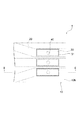
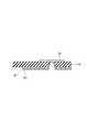
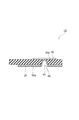
図1は本実施形態における配線基板の平面図、図2は図1のII-II線に沿った断面図、図3及び図4は本実施形態における配線基板の変形例を示す断面図である。
<< first embodiment >>
1 is a plan view of a wiring board according to the present embodiment, FIG. 2 is a cross-sectional view taken along line II-II in FIG. 1, and FIGS. 3 and 4 are cross-sectional views illustrating modifications of the wiring board according to the present embodiment. .
本実施形態における配線基板1は、例えば、コネクタ等と嵌合された状態や、異方性導電フィルム(ACF:Anisotropic Conductive Film)を介してITO(Indium Tin Oxide)からなる液晶パネルの透明電極等と圧着された状態で、携帯電話等の電子機器に組み込まれている。この配線基板1としては、フレキシブルプリント配線板(FPC:Flexible Printed Circuit)やリジッドプリント配線板(Rigid Printed Wiring Board)等を挙げることができる。 The wiring board 1 in the present embodiment is, for example, a state in which it is fitted with a connector or the like, a transparent electrode of a liquid crystal panel made of ITO (Indium Tin Oxide) through an anisotropic conductive film (ACF), etc. In a state of being crimped, it is incorporated in an electronic device such as a mobile phone. Examples of the wiring board 1 include a flexible printed circuit (FPC) and a rigid printed wiring board.
配線基板1は、図1及び図2に示すように、絶縁性基板10と、配線20と、端子部30と、バイアホール40と、導電層50と、絶縁層60と、を備えている。
As shown in FIGS. 1 and 2, the wiring board 1 includes an
絶縁性基板10は、例えば、ポリイミド(Polyimide)等の電気絶縁性を有する材料で構成されている。なお、配線基板1がリジッドプリント配線板である場合には、絶縁性基板10を、ガラスエポキシ樹脂等で構成する。この絶縁性基板10の第1の主面10aには、配線20が形成されている。一方で、絶縁性基板10において第1の主面10aとは反対側に位置する第2の主面10bには、端子部30が形成されている。
The
配線20は、例えば銅で構成されている。なお、配線20の材料は、特に限定されず、この配線20を金や銀等で構成してもよい。また、本実施形態では、図1に示すように、3本の配線20が絶縁性基板10上に形成されているが、配線20の数も特に限定されない。
The
端子部30は、配線基板10において他の電子部品(例えば、上述のコネクタや液晶パネル等)との電気的な接点となる部分であり、例えば銅で構成されている。なお、端子部30の材料は、特に限定されず、金や銀等の金属材料で構成してもよい。
The
この端子部30は、図1に示す平面視において、配線20と部分的に重複するように、絶縁性基板10の第1の主面10a上に配置されている。なお、本実施形態では、端子部30が矩形状となっているが、特に限定されない。また、本実施形態では、同図に示すように、3個の端子部30が絶縁性基板10に形成されているが、端子部30の数も特に限定されない。端子部30の数は、他の電子部品の端子数や配線20の数に応じて適宜設定することができる。
The
この端子部30の表面30aは、図2に示すように、導電性を有する端子保護層31で被覆されている。この端子保護層31は、ニッケル(Ni)めっきからなる第1の端子保護層と、金(Au)めっきからなる第2の端子保護層と、から構成されている。なお、特に図示しないが、第1の端子保護層が端子部30を直接的に被覆しており、第2の端子保護層は、第1の端子保護層を介して端子部30を被覆している。
As shown in FIG. 2, the
本実施形態では、端子保護層31を、第1の端子保護層と第2の端子保護層の2層で構成しているが、特に限定されず、端子保護層31を1層で構成してもよい。例えば、端子保護層31を第1の端子保護層のみで構成してもよい。また、端子保護層31を、ニッケルめっきや金めっきに代えて、はんだめっき、銀(Ag)めっき、錫(Sn)めっき等の金属めっきで構成してもよい。或いは、端子保護層31を、カーボンペーストや銀ペーストを印刷して硬化させることで形成してもよい。
In the present embodiment, the terminal
端子部30の裏面30bは、同図に示すように、絶縁性基板10の第2の主面10bと接している。なお、バイアホール40内では、裏面30bが絶縁性基板10から露出して、導電層50と接している。
The
バイアホール40は、配線20と端子部30とを電気的に接続するために、絶縁性基板10を貫通するが、端子部30までは貫通しない非貫通のバイアホール(Via Hole)である。このバイアホール40は、図1に示す平面視のように、配線基板1において、配線20と端子部30とが重複する位置に配置されている。
The via
バイアホール40は、図2に示すように、第1の貫通孔41と、第2の貫通孔42と、底面43と、で構成されている。
As shown in FIG. 2, the via
第1の貫通孔41は、配線20に形成されており、第2の貫通孔42と連通している。この第1の貫通孔41は、エッチングにより形成されている。
The first through
第2の貫通孔42は、絶縁性基板10に形成され、端子部30の裏面30bに至っている。この第2の貫通孔42は、例えば、レーザ加工によって形成されている。なお、第2の貫通孔42を、ウェットエッチングによって形成してもよい。
The second through
底面43は、端子部30の裏面30bで構成されており、絶縁性基板10の第2の主面10b側で第2の貫通孔42を塞いでいる。
The
このように、本実施形態におけるバイアホール40は、絶縁性基板10と配線20を貫通し、端子部30の裏面30bを底とする非貫通の穴(有底穴)となっている。
Thus, the via
導電層50は、図2に示すように、配線20からバイアホール40の内面(底面43を含む。)全体に亘って積層されており、配線20と端子部30とを電気的に接続している。この導電層50は、例えば銅めっきで構成されている。なお、導電層50の材料は、特に限定されない。例えば、導電層50を、はんだめっき、銀めっき、錫めっき等の金属めっきで構成してもよいが、配線20の材料と実質的に同一の材料であることが好ましい。
As shown in FIG. 2, the
絶縁層60は、図2に示すように、バイアホール40を塞ぐように、導電層50に積層されている。この絶縁層60としては、例えばカバーレイフィルムを挙げることができる。
As shown in FIG. 2, the insulating
この絶縁層60は、絶縁性フィルム61と、接着層62と、を有している。
The insulating
絶縁性フィルム61は、配線20及び導電層50を保護している。この絶縁性フィルム61は、例えばポリイミドで構成されている。
The insulating
接着層62は、絶縁性フィルム61と導電層50とを接着している。また、この接着層62は、バイアホール40内に進入して、バイアホール40を塞いでいる。このような接着層62は、例えばエポキシ系樹脂からなる接着剤で構成されている。
The
ここで、本実施形態における配線基板1は、1枚の絶縁性基板10に、配線20と端子部30とを形成した構成となっているが、特に限定されない。例えば、図3に示すように、配線基板1Bを、端子部30を表面に配置させた多層プリント基板で構成してもよい。この場合には、絶縁層60の絶縁性フィルムを設けず、接着層62のみで絶縁層60を構成し、この接着層62に他の絶縁性基板12を接着させてもよい。
Here, the wiring board 1 in the present embodiment has a configuration in which the
以上のように本実施形態における配線基板1は、配線20及び絶縁性基板10を貫通して、端子部30の裏面30bを底とする非貫通のバイアホール40と、バイアホール40を塞ぐ絶縁層60と、を備えている。このため、めっきの際に用いられる電解液や電子機器を取り扱う際の汗等がバイアホール40内に侵入し難くなっており、配線20や導電層50の腐食が抑制されている。これにより、配線20と端子部30との間の電気的接続の信頼性を向上させることができる。
As described above, the wiring board 1 according to the present embodiment penetrates the
また、本実施形態では、配線20と導電層50が何れも同一の材料(本例では銅)で構成されているので、配線20と導電層50とを同時にエッチングすることができる。
In the present embodiment, since both the
また、本実施形態では、端子部30の表面30aが端子保護層31で被覆されているので、端子部30の腐食が抑制されている。
Moreover, in this embodiment, since the
また、本実施形態では、絶縁性基板10をレーザ加工することで、非貫通のバイアホール40が形成されている。このため、バイアホール40を、比較的小さい径で形成することができ、端子部30の小型化及び狭ピッチ化を図ることができる。
In this embodiment, the non-penetrating via
また、配線基板1Cにおいて、図4に示すように、第1の主面10a上の配線20を、非貫通のバイアホール40とは異なるバイアホール80を介して第2の主面10b上に形成された配線90と導通させてもよい。なお、このバイアホール80は、配線20,90を導通させることができればよく、貫通していても非貫通であってもよい。或いは、バイアホール80に代えて、スルーホールで配線20,90を導通させてもよい。
In the
この配線基板1Cにおいては、絶縁性基板10の第2の主面10bにおいて、配線90のみに絶縁層60aが積層され、端子部30が露出している。このため、端子部30の表面30aを全て端子保護層31で被覆することができるので、端子部30におけるマイグレーションを抑制することができる。
In the
次に本実施形態における配線基板1の製造方法について説明する。 Next, the manufacturing method of the wiring board 1 in this embodiment is demonstrated.
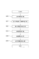
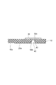
図5は本実施形態における配線基板の製造方法を示すフローチャート、図6Aは図5の端子部形成工程及び第1の貫通孔形成工程を示す断面図、図6Bは図6Aに示す配線基板を裏側から見た平面図、図6Cは図5の第2の貫通孔形成工程を示す断面図、図6Dは図5の導電層形成工程を示す断面図、図6Eは図5の配線形成工程を示す断面図、図6Fは図5の絶縁層形成工程を示す断面図である。 FIG. 5 is a flowchart showing a method of manufacturing a wiring board in the present embodiment, FIG. 6A is a cross-sectional view showing the terminal portion forming step and the first through-hole forming step of FIG. 5, and FIG. 6B is the back side of the wiring board shown in FIG. FIG. 6C is a sectional view showing the second through hole forming step of FIG. 5, FIG. 6D is a sectional view showing the conductive layer forming step of FIG. 5, and FIG. 6E shows the wiring forming step of FIG. FIG. 6F is a cross-sectional view showing the insulating layer forming step of FIG. 5.
本実施形態における配線基板1の製造方法は、図5に示すように、端子部形成工程S10と、第1の貫通孔形成工程S11と、第2の貫通孔形成工程S12と、導電層形成工程S13と、配線形成工程S14と、絶縁層形成工程S15と、端子保護層形成工程S16と、を備えている。なお、配線基板1の製造の際には、まず、絶縁性基板10の両面に導体層(銅箔)が積層された両面銅張積層板を用意する。
As shown in FIG. 5, the manufacturing method of the wiring board 1 in the present embodiment includes a terminal portion forming step S10, a first through hole forming step S11, a second through hole forming step S12, and a conductive layer forming step. S13, wiring formation process S14, insulating layer formation process S15, and terminal protective layer formation process S16 are provided. When manufacturing the wiring substrate 1, first, a double-sided copper-clad laminate in which a conductor layer (copper foil) is laminated on both sides of the insulating
端子部形成工程S10では、図6Aに示すように、絶縁性基板10の第2の主面10bに積層された導体層をエッチングすることで、端子部30を形成する。なお、この導体層は、例えば銅で構成されている。
In the terminal part forming step S10, as shown in FIG. 6A, the
このエッチングの詳細について説明すると、まず、絶縁性基板10の第2の主面10bに積層された導体層に紫外線硬化型のレジストを積層する。次いで、端子部30のパターン(開口)が形成されたマスクを通してレジストを露光する。次いで、現像して、端子部30となる部分以外に積層されたレジストを除去する。次いで、当該導体層において端子部30となる部分以外を、金属腐食性のある薬品でエッチングすることで、端子部30を形成する。最後に、端子部30上に残っているレジストを除去する。
The details of this etching will be described. First, an ultraviolet curable resist is laminated on the conductor layer laminated on the second
第1の貫通孔形成工程S11では、図6Aに示すように、端子部形成工程S10と同様の要領で、絶縁性基板10の第1の主面10aに積層された導体層11(銅箔)をエッチングすることで、第1の貫通孔41を形成する。なお、この第1の貫通孔形成工程S11では、図6Bに示す平面視において、第1の貫通孔41が端子部30と重複するように、第1の貫通孔41を導体層11に形成する。
In 1st through-hole formation process S11, as shown to FIG. 6A, the conductor layer 11 (copper foil) laminated | stacked on the 1st
第2の貫通孔形成工程S12では、図6Cに示すように、レーザ照射装置70によって絶縁性基板10に、第1の貫通孔41と連通して端子部30の裏面30bに至る第2の貫通孔42を形成する。これにより、配線基板1に非貫通のバイアホール40が形成される。
In the second through-hole forming step S12, as shown in FIG. 6C, the second through-hole reaching the
このレーザ加工の詳細について説明すると、同図に示すように、第1の貫通孔41によって露出した絶縁性基板10に、レーザ照射装置70によってレーザ光を照射する。なお、この際のレーザ光の出力は、絶縁性基板10の材料(例えばポリイミド)を加工可能ではあるが、配線20や端子部30の材料(例えば銅)を加工不可能な強さとする。これにより、導体層11がマスクとして機能し、絶縁性基板10において第1の貫通孔41によって露出した部分のみが加工される。また、第2の貫通孔42が形成されて、レーザ光が端子部30の裏面30bに至ると、端子部30がストッパとして機能し、それ以上の加工を抑制する。
The details of this laser processing will be described. As shown in the figure, the
このように、第2の貫通孔形成工程S12において、絶縁性基板10をレーザ加工することで、配線20や端子部30を加工することなく第2の貫通孔42を形成することができ、比較的小さな径のバイアホール40を形成することができる。なお、このようなレーザ加工に用いることができるレーザとしては、例えばCO2レーザ、YAGレーザ(YAG:Yttrium Aluminum Garnet)、エキシマレーザ(Excimer Laser)等を挙げることができる。
As described above, in the second through-hole forming step S12, the insulating
導電層形成工程S13では、図6Dに示すように、導体層11から第2の貫通孔42(バイアホール40)内の端子部30の裏面30bに亘って、銅からなる導電層50を積層する。これにより、端子部30と導体層11とが電気的に接続される。なお、本実施形態では、めっき法によりバイアホール40の内面に導電層50を形成する。
In the conductive layer forming step S13, as shown in FIG. 6D, a
配線形成工程S14では、図6Eに示すように、端子部形成工程S10と同様の要領で、導電層50が積層された導体層11をエッチングして、配線20を形成する。なお、導電層50を、配線20を構成する材料と実質的に同一の材料(本例では銅)で構成することで、この配線形成工程S14において、導体層50と導電層11を同時にエッチングすることができ、生産性が向上する。
In the wiring formation step S14, as shown in FIG. 6E, the
絶縁層形成工程S15では、図6Fに示すように、絶縁性フィルム61と接着層62からなるカバーレイフィルムを、バイアホール40を塞ぐように導電層50に積層して、絶縁層60を形成する。これにより、配線20及び導電層50が保護されると共に、バイアホール40が、端子部30と絶縁層60によって完全に塞がれた状態となる。なお、上述した図3に示すように、配線基板1Bを多層化する場合には、接着層62のみを導電層50に積層して、絶縁層60を形成する。
In the insulating layer forming step S15, as shown in FIG. 6F, the insulating
端子保護層形成工程S16では、端子部30の表面30aに端子保護層31を形成する。具体的には、端子部30の表面30aを、ニッケルめっきからなる第1の端子保護層で被覆して、さらに第1の端子保護層を、金めっきからなる第2の端子保護層で被覆して、端子保護層31を形成する。本実施形態では、端子部30の表面30a全体が端子保護層31で被覆されているので、端子部30における腐食やマイグレーションが抑制されている。
In the terminal protective layer forming step S <b> 16, the terminal
この端子保護層形成工程S16は、絶縁層形成工程S15前に実施してもよいが、端子保護層形成工程S16を、絶縁層形成工程S15においてバイアホール40が完全に塞がれた後に行った方が、めっき工程の際に用いられる電解液等がバイアホール40内へ侵入し難くなり、配線20や導電層50の腐食が抑制されるので好ましい。
The terminal protective layer forming step S16 may be performed before the insulating layer forming step S15, but the terminal protective layer forming step S16 is performed after the via
次に、第2実施形態について説明する。 Next, a second embodiment will be described.
<<第2実施形態>>
本実施形態における配線基板1Dでは、導電層50aの構成が第1実施形態と相違しているが、それ以外の構成については第1実施形態と同様である。以下に、第1実施形態と相違する点についてのみ説明し、第1実施形態と同様の構成である部分については同一の符号を付して説明を省略する。
<< Second Embodiment >>
In the
本実施形態における配線基板1Dの導電層50a(図8B参照)は、硬化した導電性ペーストで構成されている。この導電性ペーストとしては、銅ペースト、銀ペースト、カーボンペースト等を挙げることができる。なお、特に図示しないが、導電性ペーストをバイアホール40内に充填させて、導電層50aを形成してもよい。
The
次に、本実施形態における配線基板1Dの製造方法について説明する。
Next, a method for manufacturing the
図7は本実施形態における配線基板の製造方法を示すフローチャート、図8Aは図7の端子部形成工程及び第1の貫通孔/配線形成工程を示す断面図、図8Bは図7の導電層形成工程を示す断面図である。 7 is a flowchart showing a method of manufacturing a wiring board according to the present embodiment, FIG. 8A is a cross-sectional view showing the terminal portion forming step and the first through hole / wiring forming step of FIG. 7, and FIG. 8B is a conductive layer forming step of FIG. It is sectional drawing which shows a process.
本実施形態における配線基板1Dの製造方法は、端子部形成工程S20と、第1の貫通孔/配線形成工程S21と、第2の貫通孔形成工程S22と、導電層形成工程S23と、絶縁層形成工程S24と、端子保護層形成工程S25と、を備えている。なお、配線基板1Dの製造の際には、まず、絶縁性基板10の両面に導体層(銅箔)が積層された両面銅張積層板を用意する。
The manufacturing method of the
端子部形成工程S20では、図8Aに示すように、第1実施形態の端子部形成工程S10と同様の要領で、絶縁性基板10の第2の主面10bに形成された導体層をエッチングして、端子部30を形成する。
In the terminal portion forming step S20, as shown in FIG. 8A, the conductor layer formed on the second
第1の貫通孔/配線形成工程S21では、図8Aに示すように、第1実施形態の第1の貫通孔形成工程S11と同様の要領で、絶縁性基板10の第1の主面10aに形成された導体層をエッチングして、第1の貫通孔41を形成する。さらに、この第1の貫通孔/配線形成工程S21では、第1実施形態の配線形成工程S14と同様の要領で、絶縁性基板10の第1の主面10aに形成された導体層をエッチングして、第1の貫通孔41と同時に、配線20も形成する。
In the first through hole / wiring forming step S21, as shown in FIG. 8A, the first
第2の貫通孔形成工程S22では、第1実施形態の第2の貫通孔形成工程S12と同様の要領で、絶縁性基板10をレーザ加工して第2の貫通孔42を形成する。
In the second through-hole forming step S22, the insulating
導電層形成工程S23では、図8Bに示すように、スクリーン印刷によって配線20から第2の貫通孔42(バイアホール40)内の端子部30の裏面30bに亘って導電性ペーストを印刷する。次いで、印刷された導電性ペーストを硬化させることで、導電層50aを形成する。
In the conductive layer forming step S23, as shown in FIG. 8B, a conductive paste is printed from the
絶縁層形成工程S24では、第1実施形態の絶縁層形成工程S15と同様の要領で、導電層50a上に絶縁層を形成する。
In the insulating layer forming step S24, an insulating layer is formed on the
端子保護層形成工程S25では、第1実施形態の端子保護層形成工程S16と同様の要領で、端子30をめっきして端子保護層31を形成する。
In the terminal protective layer forming step S25, the terminal 30 is plated to form the terminal
本実施形態における導電層形成工程S23では、導電性ペーストをスクリーン印刷するので、配線20及びバイアホール40の内面のみに導電層50aを形成することができる。このため、導電層形成工程S23後に、導電層50aをエッチングする必要がなく、生産性の向上を図ることができる。
In the conductive layer forming step S23 in the present embodiment, since the conductive paste is screen-printed, the
また、本実施形態では、第1の貫通孔形成工程S21において、第1の貫通孔41と、配線20と、を同時に形成することができるので、生産性の向上を図ることができる。
In the present embodiment, since the first through
次に、第3実施形態について説明する。 Next, a third embodiment will be described.
<<第3実施形態>>
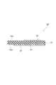
図9は本実施形態における配線基板を示す断面図である。
<< Third Embodiment >>
FIG. 9 is a cross-sectional view showing a wiring board in the present embodiment.
本実施形態における配線基板1Eでは、配線20aと、導電層50bと、の構成が第1実施形態と相違しているが、それ以外の構成については第1実施形態と同様である。以下に、第1実施形態と相違する点についてのみ説明し、第1実施形態と同様の構成である部分については同一の符号を付して説明を省略する。
In the
本実施形態における配線20a及び導電層50bは、硬化した導電性ペーストで構成されており、配線20aと導電層50bが一体的に形成されている。このような、導電性ペーストとしては、銅ペースト、銀ペースト、カーボンペースト等を挙げることができる。
The
次に、本実施形態における配線基板1Eの製造方法について説明する。
Next, a method for manufacturing the
図10は本実施形態における配線基板の製造方法を示すフローチャート、図11は図10の配線/導電層形成工程を示す断面図である。 FIG. 10 is a flowchart showing a method of manufacturing a wiring board in the present embodiment, and FIG. 11 is a cross-sectional view showing the wiring / conductive layer forming step of FIG.
本実施形態における配線基板1Eの製造方法は、端子部形成工程S30と、貫通孔形成工程S31と、配線/導電層形成工程S32と、絶縁層形成工程S33と、端子保護層形成工程S34と、を備えている。なお、配線基板1Eの製造の際には、まず、絶縁性基板10の第2の主面10bのみに導体層(銅箔)が積層された片面銅張積層板を用意する。
The manufacturing method of the
端子部形成工程S30では、図11に示すように、第1実施形態の端子部形成工程S10と同様の要領で、絶縁性基板10の第2の主面10bに形成された導体層をエッチングして、端子部30を形成する。
In the terminal portion forming step S30, as shown in FIG. 11, the conductor layer formed on the second
貫通孔形成工程S31では、第1実施形態の第2の貫通孔形成工程S12と同様の要領で、絶縁性基板10をレーザ加工して第2の貫通孔42を形成する。
In the through hole forming step S31, the insulating
配線/導電層形成工程S32では、図11に示すように、スクリーン印刷によって、導電性ペーストを、絶縁性基板10の第1の主面10aに配線20aを形成するように印刷する。さらに、この配線/導電層形成工程S32では、スクリーン印刷によって、第2の貫通孔42の内面に導電性ペーストを印刷する。次いで、このように印刷された導電性ペーストを硬化させることで、配線20a及び導電層50bを同時に形成する。
In the wiring / conductive layer forming step S32, as shown in FIG. 11, the conductive paste is printed by screen printing so as to form the
絶縁層形成工程S33では、第1実施形態の絶縁層形成工程S15と同様の要領で、導電層50b上に絶縁層を形成する。
In the insulating layer forming step S33, an insulating layer is formed on the
端子保護層形成工程S34では、第1実施形態の端子保護層形成工程S16と同様の要領で、端子30をめっきして端子保護層を形成する。
In the terminal protective layer forming step S34, the terminal protective layer is formed by plating the
このように、本実施形態における配線基板1Eの製造方法では、配線20aを形成する工程と導電層50bを形成する工程を同時に実施するので、生産性の向上を図ることができる。
As described above, in the method for manufacturing the
なお、以上に説明した実施形態は、本発明の理解を容易にするために記載されたものであって、本発明を限定するために記載されたものではない。したがって、上記の実施形態に開示された各要素は、本発明の技術的範囲に属する全ての設計変更や均等物をも含む趣旨である。 The embodiment described above is described for facilitating the understanding of the present invention, and is not described for limiting the present invention. Therefore, each element disclosed in the above embodiment is intended to include all design changes and equivalents belonging to the technical scope of the present invention.
1…配線基板
10…絶縁性基板
20…配線
30…端子部
30b…裏面
40…バイアホール
50…導電層
60…絶縁層
DESCRIPTION OF SYMBOLS 1 ... Wiring
Claims (7)
前記絶縁性基板の第1の主面に形成された配線と、
平面視において前記配線と重複するように、前記絶縁性基板の第2の主面に形成された端子部と、
前記配線と前記絶縁性基板とを貫通し、前記端子部の裏面を底とする非貫通のバイアホールと、
前記バイアホールの内面に形成され、前記配線と前記端子部とを電気的に接続する導電層と、
前記バイアホールを塞ぐように、前記導電層上に形成された絶縁層と、を備えたことを特徴とする配線基板。 An insulating substrate;
Wiring formed on the first main surface of the insulating substrate;
A terminal portion formed on the second main surface of the insulating substrate so as to overlap the wiring in a plan view;
A non-penetrating via hole penetrating the wiring and the insulating substrate and having the bottom surface of the terminal portion as a bottom;
A conductive layer formed on the inner surface of the via hole and electrically connecting the wiring and the terminal portion;
And an insulating layer formed on the conductive layer so as to close the via hole.
前記導電層は、金属めっきからなることを特徴とする配線基板。 The wiring board according to claim 1,
The wiring board, wherein the conductive layer is made of metal plating.
前記導電層は、硬化した導電性ペーストからなることを特徴とする配線基板。 The wiring board according to claim 1,
The wiring board, wherein the conductive layer is made of a hardened conductive paste.
前記バイアホールは、前記絶縁性基板をレーザ加工することで形成されていることを特徴とする配線基板。 The wiring board according to any one of claims 1 to 3,
The via hole is formed by laser processing the insulating substrate.
前記配線が形成される導体層に第1の貫通孔を形成する第1の貫通孔形成工程と、
前記第1の貫通孔と連通して前記端子部の裏面に至る第2の貫通孔を、前記絶縁性基板にレーザ加工によって形成する第2の貫通孔形成工程と、
前記第1の貫通孔及び前記第2の貫通孔の内面を金属めっきして、前記導体層と前記端子部とを電気的に接続する導電層を形成する導電層形成工程と、
前記1の貫通孔及び前記第2の貫通孔を塞ぐように、前記導電層上に絶縁層を形成する絶縁層形成工程と、を備えたことを特徴とする配線基板の製造方法。 An insulating substrate; wiring formed on the first main surface of the insulating substrate; and a terminal portion formed on the second main surface of the insulating substrate and electrically connected to the wiring. A method of manufacturing a wiring board having
A first through hole forming step of forming a first through hole in a conductor layer in which the wiring is formed;
A second through hole forming step of forming a second through hole communicating with the first through hole and reaching the back surface of the terminal portion in the insulating substrate by laser processing;
A conductive layer forming step of metal-plating inner surfaces of the first through hole and the second through hole to form a conductive layer that electrically connects the conductor layer and the terminal portion;
An insulating layer forming step of forming an insulating layer on the conductive layer so as to close the first through hole and the second through hole.
前記配線に第1の貫通孔を形成する第1の貫通孔形成工程と、
前記第1の貫通孔と連通して前記端子部の裏面に至る第2の貫通孔を、前記絶縁性基板にレーザ加工によって形成する第2の貫通孔形成工程と、
前記第1の貫通孔及び前記第2の貫通孔の内面に導電性ペーストを印刷して硬化させることで、前記配線と前記端子部とを電気的に接続する導電層を形成する導電層形成工程と、
前記1の貫通孔及び前記第2の貫通孔を塞ぐように、前記導電層上に絶縁層を形成する絶縁層形成工程と、を備えたことを特徴とする配線基板の製造方法。 An insulating substrate; wiring formed on the first main surface of the insulating substrate; and a terminal portion formed on the second main surface of the insulating substrate and electrically connected to the wiring. A method of manufacturing a wiring board having
A first through hole forming step of forming a first through hole in the wiring;
A second through hole forming step of forming a second through hole communicating with the first through hole and reaching the back surface of the terminal portion in the insulating substrate by laser processing;
A conductive layer forming step of forming a conductive layer that electrically connects the wiring and the terminal portion by printing and curing a conductive paste on the inner surfaces of the first through hole and the second through hole. When,
An insulating layer forming step of forming an insulating layer on the conductive layer so as to close the first through hole and the second through hole.
前記絶縁性基板の前記第1の主面から前記端子部の裏面に至る貫通孔を、前記絶縁性基板にレーザ加工によって形成する貫通孔形成工程と、
前記絶縁性基板の前記第1の主面に導電性ペーストを印刷して硬化させることで、前記配線を形成する配線形成工程と、
前記貫通孔の内面に前記導電性ペーストを印刷して硬化させることで、前記配線と前記端子部とを電気的に接続する導電層を形成する導電層形成工程と、
前記貫通孔を塞ぐように、前記導電層上に絶縁層を形成する絶縁層形成工程と、を備えており、
前記配線形成工程と、前記導電層形成工程と、を同時に行うことを特徴とする配線基板の製造方法。 An insulating substrate; wiring formed on the first main surface of the insulating substrate; and a terminal portion formed on the second main surface of the insulating substrate and electrically connected to the wiring. A method of manufacturing a wiring board having
A through hole forming step of forming a through hole from the first main surface of the insulating substrate to the back surface of the terminal portion in the insulating substrate by laser processing;
A wiring forming step of forming the wiring by printing and curing a conductive paste on the first main surface of the insulating substrate;
A conductive layer forming step of forming a conductive layer that electrically connects the wiring and the terminal portion by printing and curing the conductive paste on the inner surface of the through hole;
An insulating layer forming step of forming an insulating layer on the conductive layer so as to close the through hole, and
A method of manufacturing a wiring board, wherein the wiring forming step and the conductive layer forming step are performed simultaneously.
Priority Applications (1)
| Application Number | Priority Date | Filing Date | Title |
|---|---|---|---|
| JP2010065809A JP2011199103A (en) | 2010-03-23 | 2010-03-23 | Wiring board and method of manufacturing the same |
Applications Claiming Priority (1)
| Application Number | Priority Date | Filing Date | Title |
|---|---|---|---|
| JP2010065809A JP2011199103A (en) | 2010-03-23 | 2010-03-23 | Wiring board and method of manufacturing the same |
Publications (1)
| Publication Number | Publication Date |
|---|---|
| JP2011199103A true JP2011199103A (en) | 2011-10-06 |
Family
ID=44876927
Family Applications (1)
| Application Number | Title | Priority Date | Filing Date |
|---|---|---|---|
| JP2010065809A Pending JP2011199103A (en) | 2010-03-23 | 2010-03-23 | Wiring board and method of manufacturing the same |
Country Status (1)
| Country | Link |
|---|---|
| JP (1) | JP2011199103A (en) |
Cited By (2)
| Publication number | Priority date | Publication date | Assignee | Title |
|---|---|---|---|---|
| WO2013183692A1 (en) * | 2012-06-08 | 2013-12-12 | 住友電気工業株式会社 | Flexible printed wiring board and method for producing flexible printed wiring board |
| KR20140069571A (en) * | 2012-11-29 | 2014-06-10 | 엘지디스플레이 주식회사 | flexible printed circuit and display device |
-
2010
- 2010-03-23 JP JP2010065809A patent/JP2011199103A/en active Pending
Cited By (5)
| Publication number | Priority date | Publication date | Assignee | Title |
|---|---|---|---|---|
| WO2013183692A1 (en) * | 2012-06-08 | 2013-12-12 | 住友電気工業株式会社 | Flexible printed wiring board and method for producing flexible printed wiring board |
| JP2013254910A (en) * | 2012-06-08 | 2013-12-19 | Sumitomo Electric Ind Ltd | Flexible printed wiring board and manufacturing method of the same |
| CN104272882A (en) * | 2012-06-08 | 2015-01-07 | 住友电气工业株式会社 | Flexible printed wiring board and method for producing flexible printed wiring board |
| KR20140069571A (en) * | 2012-11-29 | 2014-06-10 | 엘지디스플레이 주식회사 | flexible printed circuit and display device |
| KR102035006B1 (en) * | 2012-11-29 | 2019-10-22 | 엘지디스플레이 주식회사 | flexible printed circuit and display device |
Similar Documents
| Publication | Publication Date | Title |
|---|---|---|
| TWI507096B (en) | Multilayer printed circuit board and method for manufacturing same | |
| KR100856209B1 (en) | Printed circuit board with integrated circuit and manufacturing method | |
| JPWO2009001621A1 (en) | Manufacturing method of component-embedded substrate | |
| KR101946989B1 (en) | The printed circuit board and the method for manufacturing the same | |
| JP5271627B2 (en) | Multilayer printed wiring board | |
| US8737085B2 (en) | Wiring board with a built-in component and method for manufacturing the same | |
| JP5715237B2 (en) | Flexible multilayer board | |
| JP2010232249A (en) | Multilayer printed wiring board and manufacturing method of the same | |
| TW201124007A (en) | Substrate and substrate bonding device using the same | |
| CN101959376A (en) | The manufacture method of multilayer flexible printed wiring plate and multilayer circuit basis material | |
| JP5075568B2 (en) | Shielded circuit wiring board and method for manufacturing the same | |
| JP5524315B2 (en) | Display element module using multilayer flexible printed wiring board | |
| CN209930597U (en) | Resin multilayer substrates, transmission lines, and modules | |
| JP2011199103A (en) | Wiring board and method of manufacturing the same | |
| TW200522858A (en) | Electromagnetic masking flexible circuit substrate | |
| JP2014204088A (en) | Multilayer wiring board and method of manufacturing the same | |
| CN107889356B (en) | Soft and hard composite circuit board | |
| KR20090056173A (en) | Double-sided printed circuit board and its manufacturing method | |
| KR100651474B1 (en) | Manufacturing method of pcb for embedded chip | |
| JP4347143B2 (en) | Circuit board and manufacturing method thereof | |
| KR20130033851A (en) | Multi layer pcb and manufacturing method thereof | |
| JP4863076B2 (en) | Wiring board and manufacturing method thereof | |
| JP6998744B2 (en) | Built-in component board | |
| JP2012080050A (en) | Method for manufacturing flexible wiring board | |
| JP2003060324A (en) | Printed wiring board |