JP2011238024A - Touch panel - Google Patents
Touch panel Download PDFInfo
- Publication number
- JP2011238024A JP2011238024A JP2010108878A JP2010108878A JP2011238024A JP 2011238024 A JP2011238024 A JP 2011238024A JP 2010108878 A JP2010108878 A JP 2010108878A JP 2010108878 A JP2010108878 A JP 2010108878A JP 2011238024 A JP2011238024 A JP 2011238024A
- Authority
- JP
- Japan
- Prior art keywords
- conductive layer
- voltage
- substrate
- electrodes
- touch panel
- Prior art date
- Legal status (The legal status is an assumption and is not a legal conclusion. Google has not performed a legal analysis and makes no representation as to the accuracy of the status listed.)
- Pending
Links
Images

Landscapes
- Position Input By Displaying (AREA)
Abstract
【課題】各種電子機器に用いられるタッチパネルに関し、簡易な構成で複数の押圧位置の検出が行え、多様な操作が可能なものを提供することを目的とする。
【解決手段】上基板11下面に略矩形状の上導電層12を、下基板13上面に上導電層12と所定の空隙を空けて対向する、略帯状の複数の下導電層14を形成すると共に、上導電層12の両端に下導電層14と同方向へ延出する一対の上電極15と16を、複数の下導電層14の一端にこれらを接続する下電極18を設けることによって、上導電層12両端と複数の下導電層14の電圧を検出するだけで、複数の押圧位置の検出が行えるため、上下電極の数を少なくできると共に、制御回路への接続や位置検出の演算処理も簡便なものとなり、簡易な構成で多様な操作が可能なタッチパネルを得ることができる。
【選択図】図1An object of the present invention is to provide a touch panel used in various electronic devices, which can detect a plurality of pressed positions with a simple configuration and can perform various operations.
A substantially rectangular upper conductive layer is formed on the lower surface of an upper substrate, and a plurality of substantially strip-shaped lower conductive layers are formed on the upper surface of the lower substrate to face the upper conductive layer with a predetermined gap. In addition, by providing a pair of upper electrodes 15 and 16 extending in the same direction as the lower conductive layer 14 at both ends of the upper conductive layer 12 and a lower electrode 18 connecting them to one end of the plurality of lower conductive layers 14, By detecting the voltages at both ends of the upper conductive layer 12 and the plurality of lower conductive layers 14, a plurality of pressed positions can be detected, so that the number of upper and lower electrodes can be reduced, and calculation processing for connection to the control circuit and position detection And a touch panel capable of various operations with a simple configuration can be obtained.
[Selection] Figure 1
Description
本発明は、主に各種電子機器の操作に用いられるタッチパネルに関するものである。 The present invention relates to a touch panel used mainly for operating various electronic devices.
近年、携帯電話や電子カメラ等の各種電子機器の高機能化や多様化が進むに伴い、液晶表示素子等の表示素子の前面に光透過性のタッチパネルを装着し、このタッチパネルを通して背面の表示素子の表示を見ながら、指やペン等でタッチパネルを押圧操作することによって、機器の様々な機能の切換えを行うものが増えており、多様な操作の行えるものが求められている。 In recent years, as various electronic devices such as mobile phones and electronic cameras have become highly functional and diversified, a light-transmissive touch panel is mounted on the front surface of a display element such as a liquid crystal display element, and the display element on the back side is attached through this touch panel. There are an increasing number of devices that switch various functions of a device by pressing the touch panel with a finger, a pen, or the like while viewing the display, and there is a demand for devices that can perform various operations.
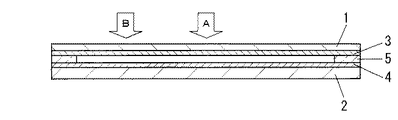
このような従来のタッチパネルについて、図8を用いて説明する。 Such a conventional touch panel will be described with reference to FIG.
なお、この図面は構成を判り易くするために、部分的に寸法を拡大して表している。 In addition, in this drawing, in order to make the configuration easy to understand, the dimensions are partially enlarged.
図8は従来のタッチパネルの断面図であり、同図において、1はフィルム状で光透過性の上基板、2はガラス等の光透過性の下基板で、上基板1の下面には略矩形状で酸化インジウム錫等の光透過性の上導電層3が、下基板2の上面には同じく下導電層4が各々ほぼ全面に形成されている。
FIG. 8 is a cross-sectional view of a conventional touch panel. In FIG. 8, 1 is a film-like upper substrate that is light-transmissive, 2 is a light-transmissive lower substrate such as glass, and the lower surface of the upper substrate 1 is substantially rectangular. A light transmissive upper
そして、下導電層4上面には絶縁樹脂によって、複数のドットスペーサ(図示せず)が所定間隔で形成されると共に、上導電層3の両端には一対の上電極(図示せず)が、下導電層4の両端には、上電極とは直交方向の一対の下電極(図示せず)が各々形成されている。
A plurality of dot spacers (not shown) are formed on the upper surface of the lower conductive layer 4 by an insulating resin at predetermined intervals, and a pair of upper electrodes (not shown) are formed at both ends of the upper
また、5は上基板1と下基板2間の外周内縁に形成された略額縁状のスペーサで、このスペーサ5の上下面または片面に塗布形成された接着剤(図示せず)によって、上基板1と下基板2の外周が貼り合わされ、上導電層3と下導電層4が所定の空隙を空けて対向するようにして、タッチパネルが構成されている。
そして、このように構成されたタッチパネルが、液晶表示素子等の表示素子の前面に配置されて電子機器に装着されると共に、一対の上電極と下電極が機器のマイコン等の制御回路(図示せず)に電気的に接続される。 The touch panel thus configured is placed on the front surface of a display element such as a liquid crystal display element and attached to an electronic device, and a pair of upper and lower electrodes are connected to a control circuit (not shown) such as a microcomputer of the device. )).
以上の構成において、タッチパネル背面の表示素子の表示に応じて、上基板1上面を指やペン等で押圧操作すると、上基板1が撓み、押圧された箇所の上導電層3が下導電層4に接触する。
In the above configuration, when the upper surface of the upper substrate 1 is pressed with a finger or a pen according to the display on the display element on the back of the touch panel, the upper substrate 1 bends, and the upper
そして、制御回路から上電極と下電極へ順次電圧が印加され、これらの電極間の電圧比によって、押圧された箇所を制御回路が検出し、機器の様々な機能の切換えが行われる。 Then, a voltage is sequentially applied from the control circuit to the upper electrode and the lower electrode, and the control circuit detects the pressed position based on a voltage ratio between these electrodes, and various functions of the device are switched.
つまり、タッチパネル背面の表示素子に、例えば複数のメニュー等が表示された状態で、所望のメニュー上の上基板1上面を矢印Aのように押圧操作すると、押圧位置に対応する上電極と下電極の各々の電圧比によって、この操作した位置を制御回路が検出し、複数のメニューの中から所望のメニューの選択等が行えるように構成されている。 That is, when, for example, a plurality of menus are displayed on the display element on the back surface of the touch panel, when the upper surface of the upper substrate 1 on the desired menu is pressed as indicated by the arrow A, the upper electrode and the lower electrode corresponding to the pressed position. The control circuit detects the operated position based on the respective voltage ratios, and a desired menu can be selected from a plurality of menus.
なお、このようなタッチパネルは上記のように、上基板1下面の略矩形状の上導電層3の両端に一対の上電極を設けると共に、下基板2上面の同じく略矩形状の下導電層4の、上電極とは直交方向の両端に一対の下電極を設け、これらの電極間の電圧比によって、押圧された箇所を検出している。
In addition, as described above, such a touch panel is provided with a pair of upper electrodes on both ends of a substantially rectangular upper
したがって、押圧された位置を検出できるのは一ヶ所のみであり、図8に示すように、例えばある指で矢印Aの箇所を押圧したままで、同時に他の指で矢印Bの箇所を押圧操作した場合、この二ヶ所の押圧位置を同時に検出することはできない。 Therefore, the pressed position can be detected only at one location, and as shown in FIG. 8, for example, while pressing the location of arrow A with one finger, the location of arrow B is simultaneously pressed with another finger. In this case, the two pressed positions cannot be detected simultaneously.
このため、例えば上導電層3と下導電層4を略矩形状ではなく、略帯状で複数の導電層、大きさにもよるが一般に十数本から数十本の導電層に形成すると共に、これらを直交方向に所定空隙で交差させて対向配置し、この各々の導電層に順次電圧を印加して、複数の押圧位置を検出することが行われている。
For this reason, for example, the upper
ただし、この場合には、複数の上下導電層の各々について、制御回路へ接続するための数十本の上下電極が必要となって、全体の外形形状が大きなものになってしまうと共に、この全ての電極に電圧を順次印加して押圧位置の検出を行う必要があるため、位置検出にも時間を要し、制御回路への接続や位置検出の演算処理も複雑なものになってしまうものであった。 However, in this case, for each of the plurality of upper and lower conductive layers, several tens of upper and lower electrodes for connection to the control circuit are required, and the overall outer shape becomes large. Since it is necessary to detect the pressed position by sequentially applying a voltage to the electrodes, it takes time to detect the position, and the connection to the control circuit and the calculation processing of the position detection become complicated. there were.
なお、この出願の発明に関連する先行技術文献情報としては、例えば、特許文献1が知られている。 As prior art document information related to the invention of this application, for example, Patent Document 1 is known.
しかしながら、上記従来のタッチパネルにおいては、略矩形状の上導電層3と下導電層4を対向させたものでは、複数の押圧位置を検出することができず、略帯状の複数の上下導電層を交差して対向させたものでは、外形形状が大きく複雑な構成になってしまうという課題があった。
However, in the conventional touch panel described above, when the substantially conductive upper
本発明は、このような従来の課題を解決するものであり、簡易な構成で複数の押圧位置の検出が行え、多様な操作が可能なタッチパネルを提供することを目的とする。 The present invention solves such a conventional problem, and an object of the present invention is to provide a touch panel that can detect a plurality of pressing positions with a simple configuration and can perform various operations.
上記目的を達成するために本発明は、上基板下面に略矩形状の上導電層を、下基板上面に上導電層と所定の空隙を空けて対向する、略帯状の複数の下導電層を形成すると共に、上導電層の両端に下導電層と同方向へ延出する一対の上電極を、複数の下導電層の一端にこれらを接続する下電極を設けてタッチパネルを構成したものであり、上導電層両端と複数の下導電層の電圧を検出するだけで、複数の押圧位置の検出が行えるため、上下電極の数も少なくてすみ、全体の外形形状が大きくなることを防ぐことができると共に、制御回路への接続や位置検出の演算処理も簡便なものとなり、簡易な構成で複数の押圧位置の検出が行え、多様な操作が可能なタッチパネルを得ることができるという作用を有するものである。 In order to achieve the above object, the present invention provides a substantially rectangular upper conductive layer on the lower surface of the upper substrate, and a plurality of substantially strip-shaped lower conductive layers facing the upper conductive layer with a predetermined gap on the upper surface of the lower substrate. A touch panel is formed by forming a pair of upper electrodes extending in the same direction as the lower conductive layer at both ends of the upper conductive layer, and providing a lower electrode connecting these at one end of the plurality of lower conductive layers. Because it is possible to detect a plurality of pressing positions by simply detecting the voltages at both ends of the upper conductive layer and the plurality of lower conductive layers, the number of upper and lower electrodes can be reduced, and the overall outer shape can be prevented from becoming large. In addition to being able to connect to the control circuit and calculation processing for position detection, it has a function of being able to detect a plurality of pressed positions with a simple configuration and obtain a touch panel capable of various operations. It is.
以上のように本発明によれば、簡易な構成で複数の押圧位置の検出が行え、多様な操作が可能なタッチパネルを実現することができるという有利な効果が得られる。 As described above, according to the present invention, it is possible to detect a plurality of pressed positions with a simple configuration and to obtain an advantageous effect that a touch panel capable of various operations can be realized.
以下、本発明の実施の形態について、図1〜図7を用いて説明する。 Hereinafter, embodiments of the present invention will be described with reference to FIGS.
なお、これらの図面は構成を判り易くするために、部分的に寸法を拡大して表している。 These drawings are partially enlarged in size for easy understanding of the configuration.
(実施の形態)
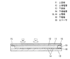
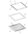
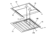
図1は本発明の一実施の形態によるタッチパネルの断面図、図2は同分解斜視図であり、同図において、11はポリエチレンテレフタレートやポリエーテルサルホン、ポリカーボネート等のフィルム状で光透過性の上基板で、この下面には略矩形状で酸化インジウム錫や酸化錫等の光透過性の上導電層12が、スパッタ法等によって形成されている。
(Embodiment)
FIG. 1 is a cross-sectional view of a touch panel according to an embodiment of the present invention, FIG. 2 is an exploded perspective view thereof, in which 11 is a film-like light-transmitting film such as polyethylene terephthalate, polyethersulfone, or polycarbonate. On the lower surface of the upper substrate, a light transmitting upper
また、13は同じくフィルム状またはガラスやアクリル等の薄板状で光透過性の下基板で、この上面には幅0.5〜10mm前後の略帯状で、酸化インジウム錫や酸化錫等の複数の光透過性の下導電層14が、0.1〜0.5mm前後の間隙を空けて形成されている。
Similarly, 13 is a film-like or thin plate such as glass or acrylic and has a light-transmitting lower substrate. On the upper surface, a substantially strip-like shape having a width of about 0.5 to 10 mm, and a plurality of indium tin oxide, tin oxide, etc. The light transmissive lower
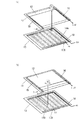
そして、下導電層14の上面にはエポキシやシリコーン等の絶縁樹脂によって複数のドットスペーサ(図示せず)が所定間隔で形成されると共に、上導電層12の左右端には下導電層14と同方向へ延出する、一対の銀やカーボン等の上電極15と16が、下導電層14の前後端には前端の複数の下電極17と、複数の下導電層14の後端を接続し、上電極15、16とは直角方向から右端方向へ延出する下電極18が各々形成されている。
A plurality of dot spacers (not shown) are formed on the upper surface of the lower
さらに、19はポリエステルやエポキシ、不織布等のスペーサで、上基板11と下基板13間の外周内縁に略額縁状に形成されると共に、このスペーサ19の上下面または片面に塗布形成されたアクリルやゴム等の接着剤(図示せず)によって、上基板11と下基板13の外周が貼り合わされ、上導電層12と複数の下導電層14が所定の空隙を空けて対向するようにして、タッチパネルが構成されている。
Further, 19 is a spacer such as polyester, epoxy, or non-woven fabric, which is formed in a substantially frame shape on the outer peripheral inner edge between the
そして、このように構成されたタッチパネルが、液晶表示素子等の表示素子の前面に配置されて電子機器に装着されると共に、一対の上電極15と16、下電極18と複数の下電極17が、コネクやタリード線(図示せず)等を介して、機器のマイコン等の制御回路(図示せず)に電気的に接続される。
The touch panel thus configured is placed on the front surface of a display element such as a liquid crystal display element and attached to an electronic device, and a pair of
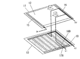
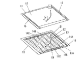
以上の構成において、タッチパネル背面の表示素子の表示に応じて、上基板11上面の、例えば図3の部分斜視図に示すように、矢印Aの箇所を指やペン等で押圧操作すると、上基板11が撓み、押圧された箇所の上導電層12が下基板13上面の下導電層14に、例えば下導電層14A後方に接触する。
In the above configuration, when the position indicated by the arrow A is pressed with a finger, a pen, or the like on the upper surface of the
そして、この時、制御回路から上導電層12両端に電圧が印加され、例えば上電極16と15に5Vの電圧が印加された場合、下導電層14Aの下電極17Aからは例えば1.5Vの電圧が検出されるため、この電圧によって矢印Aの左右方向の押圧操作位置を制御回路が検出する。
At this time, when a voltage is applied to both ends of the upper
また、この後、制御回路が電圧を印加する電極を切換え、図4(a)の部分斜視図に示すように、下電極18と17Aに5Vの電圧が印加されると、上電極16や15から例えば1.2Vの電圧が検出されるため、この電圧によって矢印Aの前後方向の押圧操作位置を制御回路が検出する。
Thereafter, when the control circuit switches the electrode to which the voltage is applied and a voltage of 5 V is applied to the
つまり、タッチパネル背面の表示素子に、例えば複数のメニュー等が表示された状態で、所望のメニュー上の上基板11上面、例えば矢印Aの箇所を押圧操作すると、上記のように、制御回路から各電極へ順次電圧が印加され、下電極17Aの電圧によって左右方向の押圧位置を、上電極16や15の電圧によって前後方向の押圧位置を制御回路が検出し、複数のメニューの中から所望のメニューの選択等が行えるように構成されている。
That is, when, for example, a plurality of menus and the like are displayed on the display element on the back surface of the touch panel, when the upper surface of the
さらに、このように矢印Aの箇所を指で押圧したままで、図3に示すように、他の指で例えば矢印Bの箇所を押圧操作すると、この箇所の上基板11も撓み、下面の上導電層12が下基板13上面の下導電層14に、例えば下導電層14D前方に接触する。
Further, when the location indicated by the arrow A is pressed with a finger in this way and the location indicated by the arrow B is pressed with another finger, for example, as shown in FIG. The
そして、この時、制御回路から上導電層12両端に、例えば上電極16と15に5Vの電圧が印加された場合、下導電層14Dの下電極17Dからは例えば3.5Vの電圧が検出されるため、この電圧によって矢印Bの左右方向の押圧操作位置を制御回路が検出する。
At this time, when a voltage of 5 V is applied to both ends of the upper
また、この後、制御回路が電圧を印加する電極を切換え、図4(b)に示すように、下電極18と17Dに5Vの電圧が印加されると、上電極16や15から例えば3.2Vの電圧が検出されるため、この電圧によって矢印Bの前後方向の押圧操作位置を制御回路が検出する。
Thereafter, when the control circuit switches the electrodes to which the voltage is applied and a voltage of 5 V is applied to the
つまり、制御回路から各電極へ順次電圧を印加して、下電極17Aの電圧によって矢印Aの左右方向の押圧位置を、下電極17Dの電圧によって矢印Bの左右方向の押圧位置を各々検出すると共に、上電極16や15の電圧によってこれらの前後方向の押圧位置を検出することで、複数の押圧位置の検出が行えるようになっている。
That is, a voltage is sequentially applied from the control circuit to each electrode, and the pressing position in the left and right direction of the arrow A is detected by the voltage of the
さらに、図5の部分斜視図に示すように、例えば矢印Cの箇所を押圧操作した後、このまま他の指で矢印Dの箇所を押圧操作した場合には、これらの箇所の上基板11が撓み、下面の上導電層12が下基板13上面の下導電層14に、例えば同じ下導電層14Bの前方と後方に各々接触する。
Furthermore, as shown in the partial perspective view of FIG. 5, for example, after pressing the location indicated by the arrow C and then pressing the location indicated by the arrow D with another finger, the
そして、この時、制御回路から上導電層12両端に、例えば上電極16と15に5Vの電圧が印加された場合、下導電層14Bの下電極17Bから検出される電圧V1は、先ず矢印Cの箇所が押圧操作された時に、例えば2.6Vの電圧が検出され、この電圧によって矢印Cの左右方向の押圧操作位置を制御回路が検出する。
At this time, when a voltage of 5 V is applied to both ends of the upper
また、この後、矢印Dの箇所も押圧された時には、下電極17Bから検出される電圧V1は、上導電層12の矢印CとDの間の抵抗が並列となるため、上記の2.6Vよりも小さな電圧値に変化し、例えば2.4Vの電圧が検出され、同時に、この矢印CとDの二箇所が押圧操作された状態では、下電極18からはさらに小さな電圧V2、例えば2.3Vの電圧が検出される。
After that, when the position of the arrow D is also pressed, the voltage V1 detected from the
つまり、このように下電極17Bから検出される電圧値V1と、下電極18から検出される電圧値V2が異なるものとなった場合、矢印CとDの二箇所の押圧操作が、一本の下導電層14B上で行われたことを制御回路が検出できるようになっている。
That is, when the voltage value V1 detected from the
そして、これらの電圧値から制御回路が、矢印Cのみが押圧された時の下電極17Bからの電圧2.6Vから、矢印Dも押圧された時の電圧2.4Vを減じた電圧値0.2Vを、下電極18からの矢印CもDも押圧された時の電圧2.3Vから減じて、矢印Dの左右方向の押圧操作位置である電圧2.1Vを算出する。
Then, from these voltage values, the control circuit subtracts a voltage value 0. 0 from the voltage 2.6V from the
さらに、この時、制御回路が電圧を印加する電極を切換え、図6の部分斜視図に示すように、下電極18と17Bに5Vの電圧が印加された場合、先ず矢印Cの箇所が押圧操作された時に、上電極16や15から検出される電圧V3は、例えば3.5Vの電圧が検出され、この電圧によって矢印Cの前後方向の押圧操作位置を制御回路が検出する。
Further, at this time, when the control circuit switches the electrodes to which the voltage is applied and a voltage of 5 V is applied to the
また、この後、矢印Dの箇所も押圧された時には、上電極16から検出される電圧V3は、下電極17Bの矢印CとDの間の抵抗が並列となるため、上記の3.5Vよりも小さな電圧値に変化し、例えば3.2Vの電圧が検出され、同時に、この矢印CとDの二箇所が押圧操作された状態では、上電極15からはさらに小さな電圧V4、例えば2.2Vの電圧が検出される。
After that, when the position of the arrow D is also pressed, the voltage V3 detected from the
すなわち、このように上電極16から検出される電圧値V3と、上電極15から検出される電圧値V4が異なるものとなった場合、上導電層12の二箇所に押圧操作が行われたことを制御回路が検出できるようになっている。
That is, when the voltage value V3 detected from the
そして、これらの電圧値から制御回路が、矢印Cのみが押圧された時の上電極16からの電圧3.5Vから、矢印Dも押圧された時の電圧3.2Vを減じた電圧値0.3Vを、上電極15からの矢印CもDも押圧された時の電圧2.2Vから減じて、矢印Dの前後方向の押圧操作位置である電圧1.9Vを算出する。
Then, from these voltage values, the control circuit subtracts the voltage value 0. 0 from the voltage 3.5 V from the
つまり、同じ下導電層14B上方の上基板11の二箇所を押圧操作した場合でも、制御回路が上記のような演算を行うことで、複数の押圧位置の検出が行えるため、複数の下導電層14をある程度大きな幅寸法で、少ない本数に形成することが可能なようになっている。
That is, even when two locations on the
すなわち、上基板11下面に略矩形状の上導電層12を、下基板13上面に上導電層12と所定の空隙を空けて対向する、略帯状の複数の下導電層14を形成すると共に、上導電層12の両端に下導電層14と同方向へ延出する一対の上電極15と16を、複数の下導電層14の一端にこれらを接続する下電極18を設けることによって、上導電層12両端と複数の下導電層14の電圧を検出するだけで、複数の押圧位置の検出を行うことが可能なように構成されている。
That is, a substantially rectangular upper
また、上記のように、複数の下導電層14をある程度大きな幅寸法で、少ない本数に形成することができるため、多様な操作を簡易な構成で行えると共に、機器の制御回路への接続や位置検出の演算処理も、簡易なものとすることができるようになっている。
In addition, as described above, since the plurality of lower
さらに、このように下導電層14をある程度大きな幅寸法に形成することで、上基板11上面を押圧し、そのまま指を左右方向へなぞるように移動するような操作を行った場合、複数の下導電層14の間隙の箇所では、制御回路が検出する電圧が階段状に変化するが、一つずつの下導電層14の幅寸法内ではなだらかな電圧変化となるため、高分解能な操作位置の検出を行うことができる。
Further, by forming the lower
なお、図7の部分斜視図に示すように、例えば矢印Eの箇所を押圧操作した状態で、押圧したまま指を矢印Fの箇所までなぞるような操作を行った場合には、上述したように、制御回路が各電極への電圧印加を順次切換え、下電極17Aや17B,17Cの電圧によって左右方向の押圧位置を、上電極16や15の電圧によって前後方向の押圧位置を制御回路が検出して、例えば点E1から点E2へ、点E3から点E4へと指が移動したことを検出する。
As shown in the partial perspective view of FIG. 7, for example, when an operation is performed in which the finger is traced to the position of the arrow F while being pressed while the position of the arrow E is pressed, as described above. The control circuit sequentially switches the voltage application to each electrode, and the control circuit detects the pressing position in the left and right direction by the voltage of the
そして、この時、各下導電層14の間隙の箇所、例えば下導電層14Aと14Bの間隙や下導電層14Bと14Cの間隙を指が移動している間は、下電極17Aや17B,17Cからは電圧が検出されないが、この場合には、例えば点E2の位置で下電極17Aから電圧が検出された後、点E3の位置で下電極17Bから電圧が検出されることによって、制御回路が点E2から点E3へ指が移動したことを判別するようになっている。
At this time, the
つまり、上述したような複数の押圧位置の検出に加え、上基板11上面を押圧し、そのまま指をなぞるように移動する操作を行った場合にも、この指の移動した軌跡を制御回路が検出可能なように構成されている。
That is, in addition to the detection of a plurality of pressing positions as described above, the control circuit detects the trajectory of the finger even when an operation of pressing the upper surface of the
なお、以上の説明では、上基板11上面を指やペン等で押圧操作し、上導電層12を撓ませる構成について説明したが、上基板11と下基板13の上下を逆に形成し、下基板13を押圧操作して下導電層14を撓ませる構成としても、本発明の実施は可能である。
In the above description, the configuration in which the upper
また、上記とは逆に、下導電層14の幅寸法を0.5〜2mm前後の小さなものに形成し、押圧する力によって上導電層12が下導電層14に接触する本数が異なるように構成して、この下導電層14の接続本数によって押圧力を検出することも可能である。
In contrast to the above, the width of the lower
このように本実施の形態によれば、上基板11下面に略矩形状の上導電層12を、下基板13上面に上導電層12と所定の空隙を空けて対向する、略帯状の複数の下導電層14を形成すると共に、上導電層12の両端に下導電層14と同方向へ延出する一対の上電極15と16を、複数の下導電層14の一端にこれらを接続する下電極18を設けることによって、上導電層12両端と複数の下導電層14の電圧を検出するだけで、複数の押圧位置の検出が行えるため、上下電極の数も少なくてすみ、全体の外形形状が大きくなることを防ぐことができると共に、制御回路への接続や位置検出の演算処理も簡便なものとなり、簡易な構成で複数の押圧位置の検出が行え、多様な操作が可能なタッチパネルを得ることができるものである。
As described above, according to the present embodiment, the substantially rectangular upper
本発明によるタッチパネルは、簡易な構成で複数の押圧位置の検出が行え、多様な操作が可能なものを得ることができるという有利な効果を有し、主に各種電子機器の操作用として有用である。 The touch panel according to the present invention has an advantageous effect that it can detect a plurality of pressed positions with a simple configuration and can obtain various operations, and is mainly useful for operation of various electronic devices. is there.
11 上基板
12 上導電層
13 下基板
14、14A、14B、14C、14D 下導電層
15、16 上電極
17、17A、17B、17C、17D、18 下電極
19 スペーサ
11
Claims (1)
Priority Applications (1)
| Application Number | Priority Date | Filing Date | Title |
|---|---|---|---|
| JP2010108878A JP2011238024A (en) | 2010-05-11 | 2010-05-11 | Touch panel |
Applications Claiming Priority (1)
| Application Number | Priority Date | Filing Date | Title |
|---|---|---|---|
| JP2010108878A JP2011238024A (en) | 2010-05-11 | 2010-05-11 | Touch panel |
Publications (1)
| Publication Number | Publication Date |
|---|---|
| JP2011238024A true JP2011238024A (en) | 2011-11-24 |
Family
ID=45325927
Family Applications (1)
| Application Number | Title | Priority Date | Filing Date |
|---|---|---|---|
| JP2010108878A Pending JP2011238024A (en) | 2010-05-11 | 2010-05-11 | Touch panel |
Country Status (1)
| Country | Link |
|---|---|
| JP (1) | JP2011238024A (en) |
Citations (2)
| Publication number | Priority date | Publication date | Assignee | Title |
|---|---|---|---|---|
| JPH05241717A (en) * | 1992-02-27 | 1993-09-21 | Gunze Ltd | Touch panel device |
| JPH0667788A (en) * | 1992-08-17 | 1994-03-11 | Seiko Epson Corp | Tablet device |
-
2010
- 2010-05-11 JP JP2010108878A patent/JP2011238024A/en active Pending
Patent Citations (2)
| Publication number | Priority date | Publication date | Assignee | Title |
|---|---|---|---|---|
| JPH05241717A (en) * | 1992-02-27 | 1993-09-21 | Gunze Ltd | Touch panel device |
| JPH0667788A (en) * | 1992-08-17 | 1994-03-11 | Seiko Epson Corp | Tablet device |
Similar Documents
| Publication | Publication Date | Title |
|---|---|---|
| US8508492B2 (en) | Touch panel and method of detecting press operation position thereon | |
| JP5407599B2 (en) | Touch panel | |
| CN105260058A (en) | Electrode sheet for pressure detection and touch input device including the same | |
| JP2012048279A (en) | Input device | |
| JP6311129B2 (en) | Touch panel | |
| CN101782827B (en) | Touch panel and method of detecting press operation position thereon | |
| JP2012003522A (en) | Touch panel | |
| US9124275B2 (en) | Touch panel | |
| JP2008027016A (en) | Touch panel | |
| CN101782822B (en) | Touch panel and method of detecting press operation position thereon | |
| JP2011238024A (en) | Touch panel | |
| JP2010191741A (en) | Touch panel | |
| KR101762279B1 (en) | Electrode sheet and touch input device for detecting pressure with temperature compensation | |
| JP2011065407A (en) | Touch panel | |
| JP5581774B2 (en) | Touch panel | |
| JP2013250836A (en) | Touch panel | |
| JP2012084037A (en) | Input device | |
| JP2012088822A (en) | Touch panel | |
| JP2010282394A (en) | Touch panel | |
| JP2014093010A (en) | Touch panel | |
| WO2015083336A1 (en) | Touch panel | |
| JP2012022358A (en) | Touch panel | |
| JP2011113453A (en) | Touch panel | |
| JP2014081870A (en) | Touch panel | |
| JP2012108835A (en) | Touch panel |
Legal Events
| Date | Code | Title | Description |
|---|---|---|---|
| A621 | Written request for application examination |
Free format text: JAPANESE INTERMEDIATE CODE: A621 Effective date: 20130509 |
|
| RD01 | Notification of change of attorney |
Free format text: JAPANESE INTERMEDIATE CODE: A7421 Effective date: 20130612 |
|
| A977 | Report on retrieval |
Free format text: JAPANESE INTERMEDIATE CODE: A971007 Effective date: 20131210 |
|
| A131 | Notification of reasons for refusal |
Free format text: JAPANESE INTERMEDIATE CODE: A131 Effective date: 20140107 |
|
| RD01 | Notification of change of attorney |
Free format text: JAPANESE INTERMEDIATE CODE: A7421 Effective date: 20140107 |
|
| A521 | Written amendment |
Free format text: JAPANESE INTERMEDIATE CODE: A523 Effective date: 20140305 |
|
| RD01 | Notification of change of attorney |
Free format text: JAPANESE INTERMEDIATE CODE: A7421 Effective date: 20140417 |
|
| A131 | Notification of reasons for refusal |
Free format text: JAPANESE INTERMEDIATE CODE: A131 Effective date: 20140924 |
|
| A711 | Notification of change in applicant |
Free format text: JAPANESE INTERMEDIATE CODE: A711 Effective date: 20141007 |
|
| A02 | Decision of refusal |
Free format text: JAPANESE INTERMEDIATE CODE: A02 Effective date: 20150421 |