JP2012005106A - 複合圧電基板の製造方法および圧電デバイス - Google Patents
複合圧電基板の製造方法および圧電デバイス Download PDFInfo
- Publication number
- JP2012005106A JP2012005106A JP2011012768A JP2011012768A JP2012005106A JP 2012005106 A JP2012005106 A JP 2012005106A JP 2011012768 A JP2011012768 A JP 2011012768A JP 2011012768 A JP2011012768 A JP 2011012768A JP 2012005106 A JP2012005106 A JP 2012005106A
- Authority
- JP
- Japan
- Prior art keywords
- piezoelectric
- substrate
- thin film
- piezoelectric thin
- support substrate
- Prior art date
- Legal status (The legal status is an assumption and is not a legal conclusion. Google has not performed a legal analysis and makes no representation as to the accuracy of the status listed.)
- Granted
Links
Images




Classifications
-
- H—ELECTRICITY
- H10—SEMICONDUCTOR DEVICES; ELECTRIC SOLID-STATE DEVICES NOT OTHERWISE PROVIDED FOR
- H10N—ELECTRIC SOLID-STATE DEVICES NOT OTHERWISE PROVIDED FOR
- H10N30/00—Piezoelectric or electrostrictive devices
- H10N30/01—Manufacture or treatment
-
- H—ELECTRICITY
- H10—SEMICONDUCTOR DEVICES; ELECTRIC SOLID-STATE DEVICES NOT OTHERWISE PROVIDED FOR
- H10N—ELECTRIC SOLID-STATE DEVICES NOT OTHERWISE PROVIDED FOR
- H10N30/00—Piezoelectric or electrostrictive devices
- H10N30/01—Manufacture or treatment
- H10N30/09—Forming piezoelectric or electrostrictive materials
- H10N30/092—Forming composite materials
-
- H—ELECTRICITY
- H03—ELECTRONIC CIRCUITRY
- H03H—IMPEDANCE NETWORKS, e.g. RESONANT CIRCUITS; RESONATORS
- H03H3/00—Apparatus or processes specially adapted for the manufacture of impedance networks, resonating circuits, resonators
- H03H3/007—Apparatus or processes specially adapted for the manufacture of impedance networks, resonating circuits, resonators for the manufacture of electromechanical resonators or networks
- H03H3/02—Apparatus or processes specially adapted for the manufacture of impedance networks, resonating circuits, resonators for the manufacture of electromechanical resonators or networks for the manufacture of piezoelectric or electrostrictive resonators or networks
-
- H—ELECTRICITY
- H03—ELECTRONIC CIRCUITRY
- H03H—IMPEDANCE NETWORKS, e.g. RESONANT CIRCUITS; RESONATORS
- H03H3/00—Apparatus or processes specially adapted for the manufacture of impedance networks, resonating circuits, resonators
- H03H3/007—Apparatus or processes specially adapted for the manufacture of impedance networks, resonating circuits, resonators for the manufacture of electromechanical resonators or networks
- H03H3/08—Apparatus or processes specially adapted for the manufacture of impedance networks, resonating circuits, resonators for the manufacture of electromechanical resonators or networks for the manufacture of resonators or networks using surface acoustic waves
-
- H—ELECTRICITY
- H03—ELECTRONIC CIRCUITRY
- H03H—IMPEDANCE NETWORKS, e.g. RESONANT CIRCUITS; RESONATORS
- H03H9/00—Networks comprising electromechanical or electro-acoustic elements; Electromechanical resonators
- H03H9/02—Details
- H03H9/02007—Details of bulk acoustic wave devices
- H03H9/02015—Characteristics of piezoelectric layers, e.g. cutting angles
-
- H—ELECTRICITY
- H03—ELECTRONIC CIRCUITRY
- H03H—IMPEDANCE NETWORKS, e.g. RESONANT CIRCUITS; RESONATORS
- H03H9/00—Networks comprising electromechanical or electro-acoustic elements; Electromechanical resonators
- H03H9/15—Constructional features of resonators consisting of piezoelectric or electrostrictive material
- H03H9/17—Constructional features of resonators consisting of piezoelectric or electrostrictive material having a single resonator
- H03H9/171—Constructional features of resonators consisting of piezoelectric or electrostrictive material having a single resonator implemented with thin-film techniques, i.e. of the film bulk acoustic resonator [FBAR] type
- H03H9/172—Means for mounting on a substrate, i.e. means constituting the material interface confining the waves to a volume
- H03H9/173—Air-gaps
-
- H—ELECTRICITY
- H03—ELECTRONIC CIRCUITRY
- H03H—IMPEDANCE NETWORKS, e.g. RESONANT CIRCUITS; RESONATORS
- H03H9/00—Networks comprising electromechanical or electro-acoustic elements; Electromechanical resonators
- H03H9/15—Constructional features of resonators consisting of piezoelectric or electrostrictive material
- H03H9/17—Constructional features of resonators consisting of piezoelectric or electrostrictive material having a single resonator
- H03H9/171—Constructional features of resonators consisting of piezoelectric or electrostrictive material having a single resonator implemented with thin-film techniques, i.e. of the film bulk acoustic resonator [FBAR] type
- H03H9/172—Means for mounting on a substrate, i.e. means constituting the material interface confining the waves to a volume
- H03H9/174—Membranes
-
- H—ELECTRICITY
- H03—ELECTRONIC CIRCUITRY
- H03H—IMPEDANCE NETWORKS, e.g. RESONANT CIRCUITS; RESONATORS
- H03H9/00—Networks comprising electromechanical or electro-acoustic elements; Electromechanical resonators
- H03H9/25—Constructional features of resonators using surface acoustic waves
-
- H—ELECTRICITY
- H10—SEMICONDUCTOR DEVICES; ELECTRIC SOLID-STATE DEVICES NOT OTHERWISE PROVIDED FOR
- H10N—ELECTRIC SOLID-STATE DEVICES NOT OTHERWISE PROVIDED FOR
- H10N30/00—Piezoelectric or electrostrictive devices
- H10N30/01—Manufacture or treatment
- H10N30/06—Forming electrodes or interconnections, e.g. leads or terminals
-
- H—ELECTRICITY
- H10—SEMICONDUCTOR DEVICES; ELECTRIC SOLID-STATE DEVICES NOT OTHERWISE PROVIDED FOR
- H10N—ELECTRIC SOLID-STATE DEVICES NOT OTHERWISE PROVIDED FOR
- H10N30/00—Piezoelectric or electrostrictive devices
- H10N30/01—Manufacture or treatment
- H10N30/07—Forming of piezoelectric or electrostrictive parts or bodies on an electrical element or another base
- H10N30/072—Forming of piezoelectric or electrostrictive parts or bodies on an electrical element or another base by laminating or bonding of piezoelectric or electrostrictive bodies
-
- H—ELECTRICITY
- H03—ELECTRONIC CIRCUITRY
- H03H—IMPEDANCE NETWORKS, e.g. RESONANT CIRCUITS; RESONATORS
- H03H3/00—Apparatus or processes specially adapted for the manufacture of impedance networks, resonating circuits, resonators
- H03H3/007—Apparatus or processes specially adapted for the manufacture of impedance networks, resonating circuits, resonators for the manufacture of electromechanical resonators or networks
- H03H3/02—Apparatus or processes specially adapted for the manufacture of impedance networks, resonating circuits, resonators for the manufacture of electromechanical resonators or networks for the manufacture of piezoelectric or electrostrictive resonators or networks
- H03H2003/021—Apparatus or processes specially adapted for the manufacture of impedance networks, resonating circuits, resonators for the manufacture of electromechanical resonators or networks for the manufacture of piezoelectric or electrostrictive resonators or networks the resonators or networks being of the air-gap type
-
- H—ELECTRICITY
- H03—ELECTRONIC CIRCUITRY
- H03H—IMPEDANCE NETWORKS, e.g. RESONANT CIRCUITS; RESONATORS
- H03H3/00—Apparatus or processes specially adapted for the manufacture of impedance networks, resonating circuits, resonators
- H03H3/007—Apparatus or processes specially adapted for the manufacture of impedance networks, resonating circuits, resonators for the manufacture of electromechanical resonators or networks
- H03H3/02—Apparatus or processes specially adapted for the manufacture of impedance networks, resonating circuits, resonators for the manufacture of electromechanical resonators or networks for the manufacture of piezoelectric or electrostrictive resonators or networks
- H03H2003/023—Apparatus or processes specially adapted for the manufacture of impedance networks, resonating circuits, resonators for the manufacture of electromechanical resonators or networks for the manufacture of piezoelectric or electrostrictive resonators or networks the resonators or networks being of the membrane type
-
- H—ELECTRICITY
- H10—SEMICONDUCTOR DEVICES; ELECTRIC SOLID-STATE DEVICES NOT OTHERWISE PROVIDED FOR
- H10N—ELECTRIC SOLID-STATE DEVICES NOT OTHERWISE PROVIDED FOR
- H10N30/00—Piezoelectric or electrostrictive devices
- H10N30/01—Manufacture or treatment
- H10N30/08—Shaping or machining of piezoelectric or electrostrictive bodies
- H10N30/082—Shaping or machining of piezoelectric or electrostrictive bodies by etching, e.g. lithography
-
- H—ELECTRICITY
- H10—SEMICONDUCTOR DEVICES; ELECTRIC SOLID-STATE DEVICES NOT OTHERWISE PROVIDED FOR
- H10P—GENERIC PROCESSES OR APPARATUS FOR THE MANUFACTURE OR TREATMENT OF DEVICES COVERED BY CLASS H10
- H10P90/00—Preparation of wafers not covered by a single main group of this subclass, e.g. wafer reinforcement
- H10P90/19—Preparing inhomogeneous wafers
- H10P90/1904—Preparing vertically inhomogeneous wafers
- H10P90/1906—Preparing SOI wafers
- H10P90/1914—Preparing SOI wafers using bonding
- H10P90/1916—Preparing SOI wafers using bonding with separation or delamination along an ion implanted layer, e.g. Smart-cut
-
- H—ELECTRICITY
- H10—SEMICONDUCTOR DEVICES; ELECTRIC SOLID-STATE DEVICES NOT OTHERWISE PROVIDED FOR
- H10P—GENERIC PROCESSES OR APPARATUS FOR THE MANUFACTURE OR TREATMENT OF DEVICES COVERED BY CLASS H10
- H10P90/00—Preparation of wafers not covered by a single main group of this subclass, e.g. wafer reinforcement
- H10P90/19—Preparing inhomogeneous wafers
- H10P90/1904—Preparing vertically inhomogeneous wafers
- H10P90/1906—Preparing SOI wafers
- H10P90/1924—Preparing SOI wafers with separation/delamination along a porous layer
-
- H—ELECTRICITY
- H10—SEMICONDUCTOR DEVICES; ELECTRIC SOLID-STATE DEVICES NOT OTHERWISE PROVIDED FOR
- H10W—GENERIC PACKAGES, INTERCONNECTIONS, CONNECTORS OR OTHER CONSTRUCTIONAL DETAILS OF DEVICES COVERED BY CLASS H10
- H10W10/00—Isolation regions in semiconductor bodies between components of integrated devices
- H10W10/10—Isolation regions comprising dielectric materials
- H10W10/181—Semiconductor-on-insulator [SOI] isolation regions, e.g. buried oxide regions of SOI wafers
-
- Y—GENERAL TAGGING OF NEW TECHNOLOGICAL DEVELOPMENTS; GENERAL TAGGING OF CROSS-SECTIONAL TECHNOLOGIES SPANNING OVER SEVERAL SECTIONS OF THE IPC; TECHNICAL SUBJECTS COVERED BY FORMER USPC CROSS-REFERENCE ART COLLECTIONS [XRACs] AND DIGESTS
- Y10—TECHNICAL SUBJECTS COVERED BY FORMER USPC
- Y10T—TECHNICAL SUBJECTS COVERED BY FORMER US CLASSIFICATION
- Y10T29/00—Metal working
- Y10T29/42—Piezoelectric device making
Landscapes
- Engineering & Computer Science (AREA)
- Physics & Mathematics (AREA)
- Acoustics & Sound (AREA)
- Manufacturing & Machinery (AREA)
- Chemical & Material Sciences (AREA)
- Composite Materials (AREA)
- Materials Engineering (AREA)
- Piezo-Electric Or Mechanical Vibrators, Or Delay Or Filter Circuits (AREA)
- Surface Acoustic Wave Elements And Circuit Networks Thereof (AREA)
Abstract
【解決手段】圧電基板1にイオンを注入してイオン注入部分2を形成する。次に、圧電基板1のイオン注入側の面に、被エッチング層3および仮基板4からなる仮支持基板を形成する。次に、仮支持基板を形成した圧電基板1を加熱し、イオン注入部分2を分離面として圧電基板1から圧電薄膜11を分離する。次に、圧電基板1から分離した圧電薄膜11に、誘電体膜12およびベース基板13からなる支持基板を形成する。ここで、仮支持基板は、圧電薄膜11との界面に作用する熱応力が支持基板よりも小さい構成材料で構成している。
【選択図】 図2
Description
一般に圧電デバイスは、圧電薄膜を支持基板によって支持した複合圧電基板として構成される(例えば特許文献1参照)。
エッチングにより仮支持基板の分離を行うことで、圧電薄膜に不要な応力や衝撃を与えることなく仮支持基板を除去でき、圧電薄膜における不具合の発生をさらに抑止できる。これにより、デバイス特性を安定させて圧電デバイスを製造することが可能になる。また、被エッチング層を除去した後の仮支持基板本体の再利用が可能になり、コスト面でも有利である。
圧電基板に注入された元素の濃度がピークになる部分を分離面として分離した圧電薄膜は、高温で熱処理を行った場合、結晶格子間に残留する残留イオンが抜けること、イオン注入時に生じた結晶格子歪が小さくなって結晶性が回復すること、により圧電性が回復する。これにより、高温での熱処理(アニール処理)を施す場合、良好なデバイス特性で圧電デバイスを製造することが可能になる。
例えば、フィルタなどでは伝搬する波の伝搬速度をコントロールしたり信頼性を向上させたりすることなどを目的に、圧電薄膜に誘電体膜を積層する場合がある。そのような構成の場合、誘電体膜としてその目的に応じた適切な誘電率の構成材料を選定する必要があるが、従来は、熱応力の制約からやはり誘電体膜として選定しうる構成材料には大幅な制限があった。本発明によれば誘電体膜を備える支持基板を加熱工程の後で圧電薄膜に形成するので、圧電薄膜と誘電体膜との界面に作用する熱応力を考慮する必要がなく、任意の線膨張係数の構成材料を選定できる。
これにより、複合圧電基板を表面波デバイスや境界波デバイスとして利用することができる。
圧電基板に注入された元素の濃度がピークになる部分を分離面として圧電基板から圧電薄膜を分離形成する方法により形成した圧電薄膜では、イオン注入側の面近傍ほど、注入イオンの衝突エネルギーが大きく結晶格子の格子間隔が伸びる傾向にあり、分離面側が凹、イオン注入面側が凸となるような応力が圧電薄膜に残留する。従来は、圧電薄膜のイオン注入側の面がメンブレン構造の空洞部に露出する構造であったため、空洞部側に圧電薄膜が凸となり、スティッキング現象(空洞部が潰れる現象)が生じ易かった。本発明によれば前述のように圧電薄膜の表裏が従来とは逆になるので、メンブレン構造の空洞部とは逆側に圧電薄膜が凸となりスティッキング現象が生じ難くなる。したがって、特性の安定した圧電デバイスを製造することが可能になる。
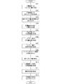
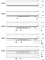
本発明の第1の実施形態に係る複合圧電基板を備える弾性表面波デバイスの製造方法を、図1〜4を参照して説明する。図1は、本実施形態に係る弾性表面波デバイスの製造方法を示すフローチャートである。図2,図3は図1のフローチャートで示される製造過程での模式構成を示す断面図である。
また、イオン注入部分で分離して単結晶基板から切り出された単結晶膜の圧電薄膜は、成膜等で形成された圧電薄膜と比べて劈開による圧電膜の破壊が起こり易く、これまでは圧電性回復のための熱処理時に線膨張係数差によって生じる応力に対して格段の配慮が必要であった。しかし本発明であれば、線膨張係数差による応力を抑制でき、容易に単結晶の圧電薄膜を得ることができる。
次に、本発明の第2の実施形態に係る複合圧電基板を備えるバルク波デバイスの製造方法を、図5〜図8を参照して説明する。図5は、本実施形態に係るバルク波デバイスの製造方法を示すフローチャートである。図6,図7は図5のフローチャートで示される製造過程での模式構成を示す断面図である。
次に、本発明の第3の実施形態に係る複合圧電基板を備えるジャイロデバイスの製造方法を、図9〜図11を参照して説明する。なお、ジャイロデバイスは、圧電振動子でシリコン振動板を屈曲振動させ、回転によってシリコン振動板に作用するコリオリの力を圧電振動子により検出する構成である。ここでは、ジャイロデバイスにおける圧電薄膜と駆動電極とからなる圧電振動子と、圧電振動子が形成されるシリコン振動板とからなる音叉型のジャイロデバイスの製造方法を例に説明する。
図9は、本実施形態に係るジャイロデバイスの製造方法の一部を示すフローチャートである。図10,図11は図9のフローチャートで示される製造過程での模式構成を示す断面図である。
2,22…イオン注入部分
3,23,43…被エッチング層
4,24,44…仮基板
10…表面波デバイス
11,31,51…圧電薄膜
12…誘電体膜
13,33…ベース基板
14…IDT電極
15…IDT電極保護膜
16…配線
17…バンプ
18…ハンダボール
30…バルク波デバイス
32A…犠牲層領域
32B…支持層領域
34,54…下部側電極
35,55…上部側電極
36…窓
38…空洞部
39…外部端子
50…ジャイロデバイス
50A…振動子
50B…シリコン振動板
56…絶縁層
57…サポート基板
圧電デバイスとして、圧電薄膜を支持基板によって支持した複合圧電基板が用いられることがある(例えば特許文献1参照)。
エッチングにより仮支持基板の分離を行うことで、圧電薄膜に不要な応力や衝撃を与えることなく仮支持基板を除去でき、圧電薄膜における不具合の発生をさらに抑止できる。これにより、デバイス特性を安定させて圧電デバイスを製造することが可能になる。また、被エッチング層を除去した後の仮支持基板本体の再利用が可能になり、コスト面でも有利である。
圧電基板に注入された元素の濃度がピークになる部分を分離面として分離した圧電薄膜は、高温で熱処理を行った場合、結晶格子間に残留する残留イオンが抜けること、イオン注入時に生じた結晶格子歪が小さくなって結晶性が回復すること、により圧電性が回復する。これにより、高温での熱処理(アニール処理)を施す場合、良好なデバイス特性で圧電デバイスを製造することが可能になる。
例えば、フィルタなどでは伝搬する波の伝搬速度をコントロールしたり信頼性を向上させたりすることなどを目的に、圧電薄膜に誘電体膜を積層する場合がある。そのような構成の場合、誘電体膜としてその目的に応じた適切な誘電率の構成材料を選定する必要があるが、従来は、熱応力の制約からやはり誘電体膜として選定しうる構成材料には大幅な制限があった。本発明によれば誘電体膜を備える支持基板を加熱工程の後で圧電薄膜に形成するので、圧電薄膜と誘電体膜との界面に作用する熱応力を考慮する必要がなく、任意の線膨張係数の構成材料を選定できる。
これにより、複合圧電基板を表面波デバイスや境界波デバイスとして利用することができる。
圧電基板に注入された元素の濃度がピークになる部分を分離面として圧電基板から圧電薄膜を分離形成する方法により形成した圧電薄膜では、イオン注入面近傍ほど、注入イオンの衝突エネルギーが大きく結晶格子の格子間隔が伸びる傾向にあり、分離面側が凹、イオン注入面側が凸となるような応力が圧電薄膜に残留する。従来は、圧電薄膜のイオン注入面側がメンブレン構造の空洞部に露出する構造であったため、空洞部側に圧電薄膜が凸となり、スティッキング現象(空洞部が潰れる現象)が生じ易かった。本発明によれば前述のように圧電薄膜の表裏が従来とは逆になるので、メンブレン構造の空洞部とは逆側に圧電薄膜が凸となりスティッキング現象が生じ難くなる。したがって、特性の安定した圧電デバイスを製造することが可能になる。
本発明の第1の実施形態に係る複合圧電基板を備える弾性表面波デバイスの製造方法を、図1〜4を参照して説明する。図1は、本実施形態に係る弾性表面波デバイスの製造方法を示すフローチャートである。図2,図3は図1のフローチャートで示される製造過程での模式構成を示す断面図である。
また、イオン注入部分で分離して単結晶基板から切り出された単結晶膜の圧電薄膜は、成膜等で形成された圧電薄膜と比べて劈開による圧電膜の破壊が起こり易く、これまでは圧電性回復のための熱処理時に線膨張係数差によって生じる応力に対して格段の配慮が必要であった。しかし本発明であれば、線膨張係数差による応力を抑制でき、容易に単結晶の圧電薄膜を得ることができる。
次に、本発明の第2の実施形態に係る複合圧電基板を備えるバルク波デバイスの製造方法を、図5〜図8を参照して説明する。図5は、本実施形態に係るバルク波デバイスの製造方法を示すフローチャートである。図6,図7は図5のフローチャートで示される製造過程での模式構成を示す断面図である。
次に、本発明の第3の実施形態に係る複合圧電基板を備えるジャイロデバイスの製造方法を、図9〜図11を参照して説明する。なお、ジャイロデバイスは、圧電振動子でシリコン振動板を屈曲振動させ、回転によってシリコン振動板に作用するコリオリの力を圧電振動子により検出する構成である。ここでは、ジャイロデバイスにおける圧電薄膜と駆動電極とからなる圧電振動子と、圧電振動子が形成されるシリコン振動板とからなる音叉型のジャイロデバイスの製造方法を例に説明する。
図9は、本実施形態に係るジャイロデバイスの製造方法の一部を示すフローチャートである。図10,図11は図9のフローチャートで示される製造過程での模式構成を示す断面図である。
2,22…イオン注入部分
3,23,43…被エッチング層
4,24,44…仮基板
10…表面波デバイス
11,31,51…圧電薄膜
12…誘電体膜
13,33…ベース基板
14…IDT電極
15…IDT電極保護膜
16…配線
17…バンプ
18…ハンダボール
30…バルク波デバイス
32A…犠牲層領域
32B…支持層領域
34,54…下部側電極
35,55…上部側電極
36…窓
38…空洞部
39…外部端子
50…ジャイロデバイス
50A…振動子
50B…シリコン振動板
56…絶縁層
57…サポート基板
Claims (10)
- 圧電薄膜を支持基板で支持する複合圧電基板の製造方法であって、
圧電基板にイオン化した元素を注入して、前記圧電基板の中に前記元素の濃度がピークになる部分を形成するイオン注入工程と、
前記圧電基板のイオン注入側の面に、前記圧電基板と同種の材料からなる、あるいは、前記圧電基板との界面に作用する熱応力が前記支持基板と前記圧電基板との界面に作用する熱応力よりも小さい、仮支持基板を形成する仮支持工程と、
前記仮支持基板を形成した前記圧電基板を加熱し、前記圧電基板に注入された元素の濃度がピークになる部分を分離面として前記圧電基板から前記圧電薄膜を分離する加熱工程と、
前記圧電基板から分離した前記圧電薄膜に前記支持基板を形成する支持工程と、
を実施する複合圧電基板の製造方法。 - 前記支持工程は、前記支持基板を、前記圧電薄膜における前記圧電基板からの分離面に形成する工程であり、
前記支持工程の後で、前記圧電薄膜のイオン注入側の面に形成した前記仮支持基板を除去する仮支持基板除去工程と、前記仮支持基板を除去したイオン注入側の面に圧電デバイスの機能電極を形成する電極形成工程とを実施する、請求項1に記載の複合圧電基板の製造方法。 - 前記仮支持基板は被エッチング層を備え、
前記仮支持基板除去工程は、前記被エッチング層をエッチングすることで前記仮支持基板を除去する、請求項1ないし2に記載の複合圧電基板の製造方法。 - 前記加熱工程は、加熱により前記圧電基板から前記圧電薄膜を分離した後で、当該圧電薄膜を分離するための加熱温度よりも高温に前記圧電薄膜を加熱するアニール工程を含む、請求項1〜3のいずれか1項に記載の複合圧電基板の製造方法。
- 前記支持基板は、前記圧電薄膜に積層される誘電体膜を備える、請求項1〜4のいずれか1項に記載の複合圧電基板の製造方法。
- 前記電極形成工程は、圧電デバイスの機能電極として前記圧電薄膜にIDT電極を形成する、請求項2〜5のいずれか1項に記載の複合圧電基板の製造方法。
- 前記支持基板は、犠牲層領域および支持層領域からなり圧電薄膜に形成されるメンブレン層と、前記メンブレン層に形成される支持基板とを備え、
前記支持工程の後で、前記犠牲層領域を除去して空洞部を形成する工程を実施する、請求項1〜6のいずれか1項に記載の複合圧電基板の製造方法。 - 圧電基板に注入されたイオン化した元素の濃度がピークになる部分を分離面として前記圧電基板から分離されることにより形成された圧電薄膜と、
前記圧電薄膜の前記分離面に形成された支持基板と、
前記圧電薄膜のイオン注入側の面に形成された機能電極と、
を備える、圧電デバイス。 - 前記機能電極がIDT電極である、請求項8に記載の圧電デバイス。
- 前記支持基板と前記圧電薄膜との間に、前記圧電薄膜を前記支持基板に支持させる支持層領域と、犠牲層領域が除去されてなる空洞部と、を設けた構成である、請求項8または9に記載の圧電デバイス。
Priority Applications (6)
| Application Number | Priority Date | Filing Date | Title |
|---|---|---|---|
| JP2011012768A JP5429200B2 (ja) | 2010-05-17 | 2011-01-25 | 複合圧電基板の製造方法および圧電デバイス |
| US13/091,167 US8872409B2 (en) | 2010-05-17 | 2011-04-21 | Method for manufacturing composite piezoelectric substrate and piezoelectric device |
| EP20110165453 EP2388840A3 (en) | 2010-05-17 | 2011-05-10 | Method for manufacturing composite piezoelectric substrate and piezoelectric device |
| KR20110043814A KR101251031B1 (ko) | 2010-05-17 | 2011-05-11 | 복합 압전기판의 제조방법 및 압전 디바이스 |
| CN201110128474.0A CN102361061B (zh) | 2010-05-17 | 2011-05-13 | 复合压电基板的制造方法及压电器件 |
| US14/492,223 US9508918B2 (en) | 2010-05-17 | 2014-09-22 | Method for manufacturing piezoelectric device with a composite piezoelectric substrate |
Applications Claiming Priority (3)
| Application Number | Priority Date | Filing Date | Title |
|---|---|---|---|
| JP2010112747 | 2010-05-17 | ||
| JP2010112747 | 2010-05-17 | ||
| JP2011012768A JP5429200B2 (ja) | 2010-05-17 | 2011-01-25 | 複合圧電基板の製造方法および圧電デバイス |
Publications (2)
| Publication Number | Publication Date |
|---|---|
| JP2012005106A true JP2012005106A (ja) | 2012-01-05 |
| JP5429200B2 JP5429200B2 (ja) | 2014-02-26 |
Family
ID=44352321
Family Applications (1)
| Application Number | Title | Priority Date | Filing Date |
|---|---|---|---|
| JP2011012768A Active JP5429200B2 (ja) | 2010-05-17 | 2011-01-25 | 複合圧電基板の製造方法および圧電デバイス |
Country Status (5)
| Country | Link |
|---|---|
| US (2) | US8872409B2 (ja) |
| EP (1) | EP2388840A3 (ja) |
| JP (1) | JP5429200B2 (ja) |
| KR (1) | KR101251031B1 (ja) |
| CN (1) | CN102361061B (ja) |
Cited By (13)
| Publication number | Priority date | Publication date | Assignee | Title |
|---|---|---|---|---|
| WO2013146374A1 (ja) * | 2012-03-26 | 2013-10-03 | 株式会社村田製作所 | 弾性波装置及びその製造方法 |
| JP2013214954A (ja) * | 2012-03-07 | 2013-10-17 | Taiyo Yuden Co Ltd | 共振子、周波数フィルタ、デュプレクサ、電子機器及び共振子の製造方法 |
| JPWO2013141184A1 (ja) * | 2012-03-23 | 2015-08-03 | 株式会社村田製作所 | 弾性波フィルタ素子及びその製造方法 |
| US20170200882A1 (en) * | 2010-09-28 | 2017-07-13 | Murata Manufacturing Co., Ltd. | Piezoelectric device and method for manufacturing piezoelectric device |
| JP2017188550A (ja) * | 2016-04-05 | 2017-10-12 | 信越化学工業株式会社 | 酸化物単結晶薄膜を備えた複合ウェーハの製造方法 |
| JP2019520753A (ja) * | 2016-06-02 | 2019-07-18 | ソイテック | 表面弾性波デバイス用のハイブリッド構造 |
| JP2020043591A (ja) * | 2019-11-21 | 2020-03-19 | 信越化学工業株式会社 | 複合ウェーハの製造方法 |
| JP2021519537A (ja) * | 2018-03-26 | 2021-08-10 | ソイテック | 高周波デバイス用の基板を製造するための方法 |
| JP2021519536A (ja) * | 2018-03-26 | 2021-08-10 | ソイテック | 圧電層を支持基板上に転写する方法 |
| WO2022071488A1 (ja) * | 2020-10-02 | 2022-04-07 | 株式会社村田製作所 | 弾性波装置 |
| JP2022084536A (ja) * | 2020-11-26 | 2022-06-07 | コミサリヤ・ア・レネルジ・アトミク・エ・オ・エネルジ・アルテルナテイブ | 大きなサーマルバジェットに適合する単結晶材料から製造された層を有するコンポーネントを製造するプロセス |
| WO2023195513A1 (ja) * | 2022-04-08 | 2023-10-12 | 株式会社村田製作所 | 弾性波装置及びその製造方法 |
| US12074581B2 (en) | 2018-10-16 | 2024-08-27 | Skyworks Solutions, Inc. | Methods and assemblies related to fabrication of acoustic wave devices |
Families Citing this family (171)
| Publication number | Priority date | Publication date | Assignee | Title |
|---|---|---|---|---|
| JP5429200B2 (ja) * | 2010-05-17 | 2014-02-26 | 株式会社村田製作所 | 複合圧電基板の製造方法および圧電デバイス |
| US8686484B2 (en) | 2011-06-10 | 2014-04-01 | Everspin Technologies, Inc. | Spin-torque magnetoresistive memory element and method of fabricating same |
| WO2013031747A1 (ja) * | 2011-09-01 | 2013-03-07 | 株式会社村田製作所 | 圧電バルク波装置及びその製造方法 |
| EP2863545B1 (en) * | 2012-06-13 | 2020-01-15 | NGK Insulators, Ltd. | Composite substrate |
| CN103091774A (zh) * | 2012-11-13 | 2013-05-08 | 东北大学秦皇岛分校 | 悬空式铌酸锂光波导 |
| JP6265915B2 (ja) * | 2012-12-26 | 2018-01-24 | 日本碍子株式会社 | 複合基板の製法 |
| CN105164919B (zh) * | 2013-03-21 | 2017-04-26 | 日本碍子株式会社 | 弹性波元件用复合基板及弹性波元件 |
| CN104078407B (zh) | 2013-03-29 | 2018-12-04 | 济南晶正电子科技有限公司 | 薄膜和制造薄膜的方法 |
| FR3004289B1 (fr) | 2013-04-08 | 2015-05-15 | Soitec Silicon On Insulator | Composant a ondes acoustiques de surface et sa methode de fabrication |
| CN104868050B (zh) * | 2014-06-09 | 2017-11-17 | 济南晶正电子科技有限公司 | 在与原始基板的热膨胀系数不同的基底上制造薄膜的方法 |
| US9805966B2 (en) * | 2014-07-25 | 2017-10-31 | Akoustis, Inc. | Wafer scale packaging |
| FR3045678B1 (fr) * | 2015-12-22 | 2017-12-22 | Soitec Silicon On Insulator | Procede de fabrication d'une couche piezoelectrique monocristalline et dispositif microelectronique, photonique ou optique comprenant une telle couche |
| FR3045677B1 (fr) | 2015-12-22 | 2019-07-19 | Soitec | Procede de fabrication d'une couche monocristalline, notamment piezoelectrique |
| US10166777B2 (en) * | 2016-04-21 | 2019-01-01 | Xerox Corporation | Method of forming piezo driver electrodes |
| CN106209003B (zh) * | 2016-07-06 | 2019-03-22 | 中国科学院上海微系统与信息技术研究所 | 利用薄膜转移技术制备薄膜体声波器件的方法 |
| US10483248B2 (en) * | 2017-03-23 | 2019-11-19 | Skyworks Solutions, Inc. | Wafer level chip scale filter packaging using semiconductor wafers with through wafer vias |
| US11323089B2 (en) | 2018-06-15 | 2022-05-03 | Resonant Inc. | Filter using piezoelectric film bonded to high resistivity silicon substrate with trap-rich layer |
| US12088281B2 (en) | 2021-02-03 | 2024-09-10 | Murata Manufacturing Co., Ltd. | Transversely-excited film bulk acoustic resonator with multi-mark interdigital transducer |
| US11509279B2 (en) | 2020-07-18 | 2022-11-22 | Resonant Inc. | Acoustic resonators and filters with reduced temperature coefficient of frequency |
| US11996827B2 (en) | 2018-06-15 | 2024-05-28 | Murata Manufacturing Co., Ltd. | Transversely-excited film bulk acoustic resonator with periodic etched holes |
| US10601392B2 (en) | 2018-06-15 | 2020-03-24 | Resonant Inc. | Solidly-mounted transversely-excited film bulk acoustic resonator |
| US10790802B2 (en) * | 2018-06-15 | 2020-09-29 | Resonant Inc. | Transversely excited film bulk acoustic resonator using rotated Y-X cut lithium niobate |
| US11936358B2 (en) | 2020-11-11 | 2024-03-19 | Murata Manufacturing Co., Ltd. | Transversely-excited film bulk acoustic resonator with low thermal impedance |
| US10637438B2 (en) | 2018-06-15 | 2020-04-28 | Resonant Inc. | Transversely-excited film bulk acoustic resonators for high power applications |
| US12040779B2 (en) | 2020-04-20 | 2024-07-16 | Murata Manufacturing Co., Ltd. | Small transversely-excited film bulk acoustic resonators with enhanced Q-factor |
| US10756697B2 (en) | 2018-06-15 | 2020-08-25 | Resonant Inc. | Transversely-excited film bulk acoustic resonator |
| US11323096B2 (en) | 2018-06-15 | 2022-05-03 | Resonant Inc. | Transversely-excited film bulk acoustic resonator with periodic etched holes |
| US11206009B2 (en) | 2019-08-28 | 2021-12-21 | Resonant Inc. | Transversely-excited film bulk acoustic resonator with interdigital transducer with varied mark and pitch |
| US12237826B2 (en) | 2018-06-15 | 2025-02-25 | Murata Manufacturing Co., Ltd. | Transversely-excited film bulk acoustic resonator with optimized electrode thickness, mark, and pitch |
| US11146232B2 (en) | 2018-06-15 | 2021-10-12 | Resonant Inc. | Transversely-excited film bulk acoustic resonator with reduced spurious modes |
| US11323090B2 (en) | 2018-06-15 | 2022-05-03 | Resonant Inc. | Transversely-excited film bulk acoustic resonator using Y-X-cut lithium niobate for high power applications |
| US11929731B2 (en) | 2018-02-18 | 2024-03-12 | Murata Manufacturing Co., Ltd. | Transversely-excited film bulk acoustic resonator with optimized electrode mark, and pitch |
| FR3078822B1 (fr) * | 2018-03-12 | 2020-02-28 | Soitec | Procede de preparation d’une couche mince de materiau ferroelectrique a base d’alcalin |
| KR102229746B1 (ko) * | 2018-03-20 | 2021-03-18 | 엔지케이 인슐레이터 엘티디 | 압전성 재료 기판과 지지 기판의 접합체 |
| DE102018107496B3 (de) * | 2018-03-28 | 2019-07-11 | RF360 Europe GmbH | Volumenschallwellenresonatorvorrichtung und Verfahren zu deren Herstellung |
| US11264966B2 (en) | 2018-06-15 | 2022-03-01 | Resonant Inc. | Solidly-mounted transversely-excited film bulk acoustic resonator with diamond layers in Bragg reflector stack |
| US12191838B2 (en) | 2018-06-15 | 2025-01-07 | Murata Manufacturing Co., Ltd. | Solidly-mounted transversely-excited film bulk acoustic device and method |
| US11901878B2 (en) | 2018-06-15 | 2024-02-13 | Murata Manufacturing Co., Ltd. | Transversely-excited film bulk acoustic resonators with two-layer electrodes with a wider top layer |
| US11909381B2 (en) | 2018-06-15 | 2024-02-20 | Murata Manufacturing Co., Ltd. | Transversely-excited film bulk acoustic resonators with two-layer electrodes having a narrower top layer |
| US10797675B2 (en) | 2018-06-15 | 2020-10-06 | Resonant Inc. | Transversely excited film bulk acoustic resonator using rotated z-cut lithium niobate |
| US11171629B2 (en) | 2018-06-15 | 2021-11-09 | Resonant Inc. | Transversely-excited film bulk acoustic resonator using pre-formed cavities |
| US12155374B2 (en) | 2021-04-02 | 2024-11-26 | Murata Manufacturing Co., Ltd. | Tiled transversely-excited film bulk acoustic resonator high power filters |
| US12155371B2 (en) | 2021-03-29 | 2024-11-26 | Murata Manufacturing Co., Ltd. | Layout of xbars with multiple sub-resonators in series |
| US12212306B2 (en) | 2018-06-15 | 2025-01-28 | Murata Manufacturing Co., Ltd. | Transversely-excited film bulk acoustic resonator with multiple diaphragm thicknesses and fabrication method |
| US12244295B2 (en) | 2018-06-15 | 2025-03-04 | Murata Manufacturing Co., Ltd. | Transversely-excited film bulk acoustic resonators with two-layer electrodes having a narrower top layer |
| US11201601B2 (en) | 2018-06-15 | 2021-12-14 | Resonant Inc. | Transversely-excited film bulk acoustic resonator with multiple diaphragm thicknesses and fabrication method |
| US11323091B2 (en) | 2018-06-15 | 2022-05-03 | Resonant Inc. | Transversely-excited film bulk acoustic resonator with diaphragm support pedestals |
| US12301212B2 (en) | 2018-06-15 | 2025-05-13 | Murata Manufacturing Co., Ltd. | XBAR resonators with non-rectangular diaphragms |
| US10917072B2 (en) | 2019-06-24 | 2021-02-09 | Resonant Inc. | Split ladder acoustic wave filters |
| US12224732B2 (en) | 2018-06-15 | 2025-02-11 | Murata Manufacturing Co., Ltd. | Solidly-mounted transversely-excited film bulk acoustic resonators and filters for 27 GHz communications bands |
| US10992284B2 (en) | 2018-06-15 | 2021-04-27 | Resonant Inc. | Filter using transversely-excited film bulk acoustic resonators with multiple frequency setting layers |
| US11967945B2 (en) | 2018-06-15 | 2024-04-23 | Murata Manufacturing Co., Ltd. | Transversly-excited film bulk acoustic resonators and filters |
| US12040781B2 (en) | 2018-06-15 | 2024-07-16 | Murata Manufacturing Co., Ltd. | Transversely-excited film bulk acoustic resonator package |
| US10998882B2 (en) | 2018-06-15 | 2021-05-04 | Resonant Inc. | XBAR resonators with non-rectangular diaphragms |
| US12463619B2 (en) | 2018-06-15 | 2025-11-04 | Murata Manufacturing Co., Ltd. | Filter device |
| US12095446B2 (en) | 2018-06-15 | 2024-09-17 | Murata Manufacturing Co., Ltd. | Transversely-excited film bulk acoustic resonator with optimized electrode thickness, mark, and pitch |
| US11949402B2 (en) | 2020-08-31 | 2024-04-02 | Murata Manufacturing Co., Ltd. | Resonators with different membrane thicknesses on the same die |
| US10819309B1 (en) | 2019-04-05 | 2020-10-27 | Resonant Inc. | Transversely-excited film bulk acoustic resonator package and method |
| US12009798B2 (en) | 2018-06-15 | 2024-06-11 | Murata Manufacturing Co., Ltd. | Transversely-excited film bulk acoustic resonators with electrodes having irregular hexagon cross-sectional shapes |
| US12218650B2 (en) | 2018-06-15 | 2025-02-04 | Murata Manufacturing Co., Ltd. | Transversely-excited film bulk acoustic resonator |
| US11888463B2 (en) | 2018-06-15 | 2024-01-30 | Murata Manufacturing Co., Ltd. | Multi-port filter using transversely-excited film bulk acoustic resonators |
| US11323095B2 (en) | 2018-06-15 | 2022-05-03 | Resonant Inc. | Rotation in XY plane to suppress spurious modes in XBAR devices |
| US12184261B2 (en) | 2018-06-15 | 2024-12-31 | Murata Manufacturing Co., Ltd. | Transversely-excited film bulk acoustic resonator with a cavity having round end zones |
| US11374549B2 (en) | 2018-06-15 | 2022-06-28 | Resonant Inc. | Filter using transversely-excited film bulk acoustic resonators with divided frequency-setting dielectric layers |
| US11146238B2 (en) | 2018-06-15 | 2021-10-12 | Resonant Inc. | Film bulk acoustic resonator fabrication method |
| US11996822B2 (en) | 2018-06-15 | 2024-05-28 | Murata Manufacturing Co., Ltd. | Wide bandwidth time division duplex transceiver |
| US11329628B2 (en) | 2020-06-17 | 2022-05-10 | Resonant Inc. | Filter using lithium niobate and lithium tantalate transversely-excited film bulk acoustic resonators |
| US11916539B2 (en) | 2020-02-28 | 2024-02-27 | Murata Manufacturing Co., Ltd. | Split-ladder band N77 filter using transversely-excited film bulk acoustic resonators |
| US12375056B2 (en) | 2018-06-15 | 2025-07-29 | Murata Manufacturing Co., Ltd. | Transversely-excited film bulk acoustic resonators |
| US11349452B2 (en) | 2018-06-15 | 2022-05-31 | Resonant Inc. | Transversely-excited film bulk acoustic filters with symmetric layout |
| US10826462B2 (en) | 2018-06-15 | 2020-11-03 | Resonant Inc. | Transversely-excited film bulk acoustic resonators with molybdenum conductors |
| US11349450B2 (en) | 2018-06-15 | 2022-05-31 | Resonant Inc. | Symmetric transversely-excited film bulk acoustic resonators with reduced spurious modes |
| US11728785B2 (en) | 2018-06-15 | 2023-08-15 | Murata Manufacturing Co., Ltd. | Transversely-excited film bulk acoustic resonator using pre-formed cavities |
| US12283944B2 (en) | 2018-06-15 | 2025-04-22 | Murata Manufacturing Co., Ltd. | Transversely-excited film bulk acoustic resonator with recessed rotated-Y-X cut lithium niobate |
| US11876498B2 (en) | 2018-06-15 | 2024-01-16 | Murata Manufacturing Co., Ltd. | Transversely-excited film bulk acoustic resonator with multiple diaphragm thicknesses and fabrication method |
| US11228296B2 (en) | 2018-06-15 | 2022-01-18 | Resonant Inc. | Transversely-excited film bulk acoustic resonator with a cavity having a curved perimeter |
| US11996825B2 (en) | 2020-06-17 | 2024-05-28 | Murata Manufacturing Co., Ltd. | Filter using lithium niobate and rotated lithium tantalate transversely-excited film bulk acoustic resonators |
| US12081187B2 (en) | 2018-06-15 | 2024-09-03 | Murata Manufacturing Co., Ltd. | Transversely-excited film bulk acoustic resonator |
| US12191837B2 (en) | 2018-06-15 | 2025-01-07 | Murata Manufacturing Co., Ltd. | Solidly-mounted transversely-excited film bulk acoustic device |
| US12170516B2 (en) | 2018-06-15 | 2024-12-17 | Murata Manufacturing Co., Ltd. | Filters using transversly-excited film bulk acoustic resonators with frequency-setting dielectric layers |
| US12237827B2 (en) | 2018-06-15 | 2025-02-25 | Murata Manufacturing Co., Ltd. | Solidly-mounted transversely-excited film bulk acoustic filters with multiple piezoelectric plate thicknesses |
| US12149227B2 (en) | 2018-06-15 | 2024-11-19 | Murata Manufacturing Co., Ltd. | Transversely-excited film bulk acoustic resonator package |
| US12119805B2 (en) | 2018-06-15 | 2024-10-15 | Murata Manufacturing Co., Ltd. | Substrate processing and membrane release of transversely-excited film bulk acoustic resonator using a sacrificial tub |
| US12095441B2 (en) | 2018-06-15 | 2024-09-17 | Murata Manufacturing Co., Ltd. | Transversely excited film bulk acoustic resonator with recessed interdigital transducer fingers |
| US12119808B2 (en) | 2018-06-15 | 2024-10-15 | Murata Manufacturing Co., Ltd. | Transversely-excited film bulk acoustic resonator package |
| US12021496B2 (en) | 2020-08-31 | 2024-06-25 | Murata Manufacturing Co., Ltd. | Resonators with different membrane thicknesses on the same die |
| US12113512B2 (en) | 2021-03-29 | 2024-10-08 | Murata Manufacturing Co., Ltd. | Layout of XBARs with multiple sub-resonators in parallel |
| CN108707970B (zh) * | 2018-08-07 | 2023-09-26 | 济南晶正电子科技有限公司 | 微米级单晶薄膜 |
| KR20200030478A (ko) * | 2018-09-12 | 2020-03-20 | 스카이워크스 글로벌 피티이. 엘티디. | 벌크 음향파 공진기를 위한 리세스 프레임 구조체 |
| DE112019005403T5 (de) | 2018-10-31 | 2021-07-15 | Resonant Inc. | Fest montierter transversal angeregter akustischer filmvolumenresonator |
| DE102018131946A1 (de) * | 2018-12-12 | 2020-06-18 | RF360 Europe GmbH | Dünnfilm-SAW-Vorrichtung |
| CN109665488B (zh) * | 2018-12-29 | 2024-07-19 | 杭州士兰集成电路有限公司 | Mems器件及其制造方法 |
| US11901873B2 (en) | 2019-03-14 | 2024-02-13 | Murata Manufacturing Co., Ltd. | Transversely-excited film bulk acoustic resonator with partial BRAGG reflectors |
| CN113615083B (zh) | 2019-03-14 | 2024-10-15 | 株式会社村田制作所 | 带有半λ介电层的横向激励的薄膜体声学谐振器 |
| US10911021B2 (en) | 2019-06-27 | 2021-02-02 | Resonant Inc. | Transversely-excited film bulk acoustic resonator with lateral etch stop |
| US12034423B2 (en) | 2019-06-27 | 2024-07-09 | Murata Manufacturing Co., Ltd | XBAR frontside etch process using polysilicon sacrificial layer |
| US11329625B2 (en) | 2019-07-18 | 2022-05-10 | Resonant Inc. | Film bulk acoustic sensors using thin LN-LT layer |
| US10862454B1 (en) | 2019-07-18 | 2020-12-08 | Resonant Inc. | Film bulk acoustic resonators in thin LN-LT layers |
| KR102319996B1 (ko) * | 2020-01-03 | 2021-11-01 | (주)와이솔 | 표면탄성파 소자 및 표면탄성파 소자의 제조방법 |
| US12255625B2 (en) | 2020-02-28 | 2025-03-18 | Murata Manufacturing Co., Ltd. | Filter using transversely-excited film bulk acoustic resonators with inductively coupled sub-resonators |
| US12506462B2 (en) | 2020-02-28 | 2025-12-23 | Murata Manufacturing Co., Ltd. | Transversely-excited film bulk acoustic resonator with multi-pitch interdigital transducer |
| FR3108439B1 (fr) | 2020-03-23 | 2022-02-11 | Soitec Silicon On Insulator | Procede de fabrication d’une structure empilee |
| US12341493B2 (en) | 2020-04-20 | 2025-06-24 | Murata Manufacturing Co., Ltd. | Low loss transversely-excited film bulk acoustic resonators and filters |
| US12341490B2 (en) | 2020-04-20 | 2025-06-24 | Murata Manufacturing Co., Ltd. | Low loss transversely-excited film bulk acoustic resonators and filters |
| US12278617B2 (en) | 2020-04-20 | 2025-04-15 | Murata Manufacturing Co., Ltd. | High Q solidly-mounted transversely-excited film bulk acoustic resonators |
| US11811391B2 (en) | 2020-05-04 | 2023-11-07 | Murata Manufacturing Co., Ltd. | Transversely-excited film bulk acoustic resonator with etched conductor patterns |
| US11469733B2 (en) | 2020-05-06 | 2022-10-11 | Resonant Inc. | Transversely-excited film bulk acoustic resonators with interdigital transducer configured to reduce diaphragm stress |
| US12074584B2 (en) | 2020-05-28 | 2024-08-27 | Murata Manufacturing Co., Ltd. | Transversely-excited film bulk acoustic resonators with two-layer electrodes |
| US12267062B2 (en) | 2020-06-17 | 2025-04-01 | Murata Manufacturing Co., Ltd. | Transversely-excited film bulk acoustic resonators with three-layer electrodes |
| US10992282B1 (en) | 2020-06-18 | 2021-04-27 | Resonant Inc. | Transversely-excited film bulk acoustic resonators with electrodes having a second layer of variable width |
| US11742828B2 (en) | 2020-06-30 | 2023-08-29 | Murata Manufacturing Co., Ltd. | Transversely-excited film bulk acoustic resonator with symmetric diaphragm |
| US11482981B2 (en) | 2020-07-09 | 2022-10-25 | Resonanat Inc. | Transversely-excited film bulk acoustic resonators with piezoelectric diaphragm supported by piezoelectric substrate |
| CN111883647B (zh) * | 2020-07-23 | 2021-05-25 | 中国科学院上海微系统与信息技术研究所 | 一种压电薄膜的制备方法、压电薄膜及声表面波滤波器 |
| US11264969B1 (en) | 2020-08-06 | 2022-03-01 | Resonant Inc. | Transversely-excited film bulk acoustic resonator comprising small cells |
| US11271539B1 (en) | 2020-08-19 | 2022-03-08 | Resonant Inc. | Transversely-excited film bulk acoustic resonator with tether-supported diaphragm |
| US11671070B2 (en) | 2020-08-19 | 2023-06-06 | Murata Manufacturing Co., Ltd. | Transversely-excited film bulk acoustic resonators using multiple dielectric layer thicknesses to suppress spurious modes |
| US11894835B2 (en) | 2020-09-21 | 2024-02-06 | Murata Manufacturing Co., Ltd. | Sandwiched XBAR for third harmonic operation |
| US11728784B2 (en) | 2020-10-05 | 2023-08-15 | Murata Manufacturing Co., Ltd. | Transversely-excited film bulk acoustic resonator matrix filters with split die sub-filters |
| US11405017B2 (en) | 2020-10-05 | 2022-08-02 | Resonant Inc. | Acoustic matrix filters and radios using acoustic matrix filters |
| US11658639B2 (en) | 2020-10-05 | 2023-05-23 | Murata Manufacturing Co., Ltd. | Transversely-excited film bulk acoustic resonator matrix filters with noncontiguous passband |
| US11476834B2 (en) | 2020-10-05 | 2022-10-18 | Resonant Inc. | Transversely-excited film bulk acoustic resonator matrix filters with switches in parallel with sub-filter shunt capacitors |
| US11405019B2 (en) | 2020-10-05 | 2022-08-02 | Resonant Inc. | Transversely-excited film bulk acoustic resonator matrix filters |
| US11929733B2 (en) | 2020-10-05 | 2024-03-12 | Murata Manufacturing Co., Ltd. | Transversely-excited film bulk acoustic resonator matrix filters with input and output impedances matched to radio frequency front end elements |
| US11463066B2 (en) | 2020-10-14 | 2022-10-04 | Resonant Inc. | Transversely-excited film bulk acoustic resonators with piezoelectric diaphragm supported by piezoelectric substrate |
| CN112259678B (zh) * | 2020-10-19 | 2022-07-19 | 济南晶正电子科技有限公司 | 一种用于改善薄膜层炸裂的方法及薄膜材料 |
| US12119806B2 (en) | 2020-10-30 | 2024-10-15 | Murata Manufacturing Co., Ltd. | Transversely-excited film bulk acoustic resonator with spiral interdigitated transducer fingers |
| US12003226B2 (en) | 2020-11-11 | 2024-06-04 | Murata Manufacturing Co., Ltd | Transversely-excited film bulk acoustic resonator with low thermal impedance |
| US12255617B2 (en) | 2020-11-11 | 2025-03-18 | Murata Manufacturing Co., Ltd. | Solidly-mounted transversely-excited film bulk acoustic resonators with low thermal impedance |
| US12431856B2 (en) | 2020-11-12 | 2025-09-30 | Murata Manufacturing Co., Ltd. | Transversely-excited film bulk acoustic resonator with reduced loss in the aperture direction |
| US12255626B2 (en) | 2020-11-13 | 2025-03-18 | Murata Manufacturing Co., Ltd. | Solidly-mounted transversely-excited film bulk acoustic filters with excess piezoelectric material removed |
| US11496113B2 (en) | 2020-11-13 | 2022-11-08 | Resonant Inc. | XBAR devices with excess piezoelectric material removed |
| US12028039B2 (en) | 2020-11-13 | 2024-07-02 | Murata Manufacturing Co., Ltd. | Forming XBAR devices with excess piezoelectric material removed |
| US12362725B2 (en) | 2020-11-13 | 2025-07-15 | Murata Manufacturing Co., Ltd. | Transversely-excited film bulk acoustic filters with excess piezoelectric material removed |
| US11405020B2 (en) | 2020-11-26 | 2022-08-02 | Resonant Inc. | Transversely-excited film bulk acoustic resonators with structures to reduce acoustic energy leakage |
| US11239816B1 (en) | 2021-01-15 | 2022-02-01 | Resonant Inc. | Decoupled transversely-excited film bulk acoustic resonators |
| US12126318B2 (en) | 2021-01-15 | 2024-10-22 | Murata Manufacturing Co., Ltd. | Filters using decoupled transversely-excited film bulk acoustic resonators |
| US12166468B2 (en) | 2021-01-15 | 2024-12-10 | Murata Manufacturing Co., Ltd. | Decoupled transversely-excited film bulk acoustic resonators for high power filters |
| US12463615B2 (en) | 2021-01-21 | 2025-11-04 | Murata Manufacturing Co., Ltd | Transversely-excited film bulk acoustic resonators with improved coupling and reduced energy leakage |
| US12113510B2 (en) | 2021-02-03 | 2024-10-08 | Murata Manufacturing Co., Ltd. | Transversely-excited film bulk acoustic resonators with multiple piezoelectric membrane thicknesses on the same chip |
| US12308826B2 (en) | 2021-02-03 | 2025-05-20 | Murata Manufacturing Co., Ltd. | Bandpass filters using transversely-excited film bulk acoustic resonators |
| US12308825B2 (en) | 2021-02-12 | 2025-05-20 | Murata Manufacturing Co., Ltd | Transversely-excited film bulk acoustic resonators with narrow gaps between busbars and ends of interdigital transducer fingers |
| US12348216B2 (en) | 2021-03-24 | 2025-07-01 | Murata Manufacturing Co., Ltd. | Acoustic filters with shared acoustic tracks and cascaded series resonators |
| US12289099B2 (en) | 2021-03-24 | 2025-04-29 | Murata Manufacturing Co., Ltd. | Acoustic filters with shared acoustic tracks for series and shunt resonators |
| US12355426B2 (en) | 2021-03-24 | 2025-07-08 | Murata Manufacturing Co., Ltd. | Acoustic filters with shared acoustic tracks |
| US12126328B2 (en) | 2021-03-24 | 2024-10-22 | Murata Manufacturing Co., Ltd. | Acoustic filters with shared acoustic tracks |
| US12341492B2 (en) | 2021-03-29 | 2025-06-24 | Murata Manufacturing Co., Ltd. | Transversely-excited film bulk acoustic resonators with busbar side edges that form angles with a perimeter of the cavity |
| CN120454674A (zh) | 2021-03-30 | 2025-08-08 | 株式会社村田制作所 | 使用横向激发薄膜体声谐振器的用于6 GHz WI-FI的滤波器 |
| US12224735B2 (en) | 2021-03-30 | 2025-02-11 | Murata Manufacturing Co., Ltd. | Diplexer using decoupled transversely-excited film bulk acoustic resonators |
| US12249971B2 (en) | 2021-04-02 | 2025-03-11 | Murata Manufacturing Co., Ltd. | Transversely-excited film bulk acoustic resonators with solidly mounted resonator (SMR) pedestals |
| US12237823B2 (en) | 2021-04-02 | 2025-02-25 | Murata Manufacturing Co., Ltd. | Transversely-excited film bulk acoustic resonators with solidly mounted resonator (SMR) pedestals |
| US12255633B2 (en) | 2021-04-16 | 2025-03-18 | Murata Manufacturing Co., Ltd. | Filter using transversely-excited film bulk acoustic resonators |
| US12126316B2 (en) | 2021-04-16 | 2024-10-22 | Murata Manufacturing Co., Ltd | Transversely-excited film bulk acoustic resonator |
| US12160220B2 (en) | 2021-04-30 | 2024-12-03 | Murata Manufacturing Co., Ltd. | Transversely-excited film bulk acoustic resonator with oxide strip acoustic confinement structures |
| US12255607B2 (en) | 2021-04-30 | 2025-03-18 | Murata Manufacturing Co., Ltd. | Transversely-excited film bulk acoustic resonator with buried oxide strip acoustic confinement structures |
| US12057823B2 (en) | 2021-05-07 | 2024-08-06 | Murata Manufacturing Co., Ltd. | Transversely-excited film bulk acoustic resonator with concentric interdigitated transducer fingers |
| US12075700B2 (en) | 2021-05-07 | 2024-08-27 | Murata Manufacturing Co., Ltd. | Transversely-excited film bulk acoustic resonator fabrication using polysilicon pillars |
| US12170513B2 (en) | 2021-06-30 | 2024-12-17 | Murata Manufacturing Co., Ltd. | Transversely-excited film bulk acoustic resonator with reduced substrate to contact bump thermal resistance |
| US12603639B2 (en) | 2021-08-02 | 2026-04-14 | Murata Manufacturing Co., Ltd. | Metal cavity for transversely-excited film bulk acoustic resonator (XBAR) |
| CN113810009B (zh) * | 2021-09-22 | 2023-03-24 | 武汉敏声新技术有限公司 | 薄膜体声波谐振器及其制备方法、薄膜体声波滤波器 |
| US12456962B2 (en) | 2021-09-24 | 2025-10-28 | Murata Manufacturing Co., Ltd. | Transversely-excited film bulk acoustic resonators wafer-level packaging using a dielectric cover |
| US12225387B2 (en) | 2021-09-29 | 2025-02-11 | Murata Manufacturing Co., Ltd. | Communications device with concurrent operation in 5GHZ and 6GHZ U-NII frequency ranges |
| US12451864B2 (en) | 2021-09-29 | 2025-10-21 | Murata Manufacturing Co., Ltd. | Transversely-excited film bulk acoustic resonators with curved shaped ends of fingers or opposing busbars |
| US12407326B2 (en) | 2021-11-04 | 2025-09-02 | Murata Manufacturing Co., Ltd. | Stacked die transversely-excited film bulk acoustic resonator (XBAR) filters |
| US12494768B2 (en) | 2021-12-28 | 2025-12-09 | Murata Manufacturing Co., Ltd. | Transversely-excited film bulk acoustic resonators with gap dielectric stripes in busbar-electrode gaps |
| US12424999B2 (en) | 2021-12-28 | 2025-09-23 | Murata Manufacturing Co., Ltd. | Transversely-excited film bulk acoustic resonators with gap dielectric stripes in busbar-electrode gaps |
| US12413196B2 (en) | 2022-02-16 | 2025-09-09 | Murata Manufacturing Co., Ltd. | Tuning acoustic resonators with back-side coating |
| US12549151B2 (en) | 2022-04-12 | 2026-02-10 | Murata Manufacturing Co., Ltd. | Transversely-excited film bulk acoustic resonator with thick dielectric layer for improved coupling |
| US12489417B2 (en) | 2022-04-12 | 2025-12-02 | Murata Manufacturing Co., Ltd. | Ladder filter with transversely-excited film bulk acoustic resonators having different pitches |
| CN114553163B (zh) * | 2022-04-28 | 2022-09-06 | 深圳新声半导体有限公司 | 体声波谐振器的制造方法 |
| US12489415B2 (en) | 2022-10-19 | 2025-12-02 | Murata Manufacturing Co., Ltd. | Acoustic resonator lid for thermal transport |
| CN117156947B (zh) * | 2023-10-31 | 2024-02-20 | 北京青禾晶元半导体科技有限责任公司 | 一种复合压电衬底的制备方法 |
Citations (4)
| Publication number | Priority date | Publication date | Assignee | Title |
|---|---|---|---|---|
| JP2008048040A (ja) * | 2006-08-11 | 2008-02-28 | Matsushita Electric Ind Co Ltd | 圧電薄膜共振器およびその製造方法 |
| WO2009081651A1 (ja) * | 2007-12-25 | 2009-07-02 | Murata Manufacturing Co., Ltd. | 複合圧電基板の製造方法 |
| JP2010109949A (ja) * | 2008-10-31 | 2010-05-13 | Murata Mfg Co Ltd | 電子デバイスの製造方法および圧電デバイスの製造方法 |
| JP2010109950A (ja) * | 2008-10-31 | 2010-05-13 | Murata Mfg Co Ltd | 圧電デバイスの製造方法 |
Family Cites Families (13)
| Publication number | Priority date | Publication date | Assignee | Title |
|---|---|---|---|---|
| JPH0590893A (ja) * | 1991-09-26 | 1993-04-09 | Sumitomo Electric Ind Ltd | 表面弾性波素子 |
| JPH06303073A (ja) * | 1993-02-17 | 1994-10-28 | Fujitsu Ltd | 弾性表面波デバイスとその製造方法 |
| JPH07142954A (ja) * | 1993-11-15 | 1995-06-02 | Murata Mfg Co Ltd | 圧電薄膜複合共振子およびその製造方法 |
| FR2714200B1 (fr) * | 1993-11-25 | 1996-12-27 | Fujitsu Ltd | Dispositif à onde acoustique de surface et son procédé de fabrication. |
| SG65697A1 (en) * | 1996-11-15 | 1999-06-22 | Canon Kk | Process for producing semiconductor article |
| US5909627A (en) * | 1998-05-18 | 1999-06-01 | Philips Electronics North America Corporation | Process for production of thin layers of semiconductor material |
| FR2788176B1 (fr) * | 1998-12-30 | 2001-05-25 | Thomson Csf | Dispositif a ondes acoustiques guidees dans une fine couche de materiau piezo-electrique collee par une colle moleculaire sur un substrat porteur et procede de fabrication |
| US6767749B2 (en) * | 2002-04-22 | 2004-07-27 | The United States Of America As Represented By The Secretary Of The Navy | Method for making piezoelectric resonator and surface acoustic wave device using hydrogen implant layer splitting |
| US20080165565A1 (en) * | 2004-01-12 | 2008-07-10 | Eidgenossische Technische Hochschule Zurich | Ferroelectric Thin Films and Devices Comprising Thin Ferroelectric Films |
| FR2914493B1 (fr) | 2007-03-28 | 2009-08-07 | Soitec Silicon On Insulator | Substrat demontable. |
| FR2925221B1 (fr) | 2007-12-17 | 2010-02-19 | Commissariat Energie Atomique | Procede de transfert d'une couche mince |
| JP4636292B2 (ja) * | 2008-08-27 | 2011-02-23 | 株式会社村田製作所 | 電子部品及び電子部品の製造方法 |
| JP5429200B2 (ja) * | 2010-05-17 | 2014-02-26 | 株式会社村田製作所 | 複合圧電基板の製造方法および圧電デバイス |
-
2011
- 2011-01-25 JP JP2011012768A patent/JP5429200B2/ja active Active
- 2011-04-21 US US13/091,167 patent/US8872409B2/en active Active
- 2011-05-10 EP EP20110165453 patent/EP2388840A3/en not_active Withdrawn
- 2011-05-11 KR KR20110043814A patent/KR101251031B1/ko active Active
- 2011-05-13 CN CN201110128474.0A patent/CN102361061B/zh active Active
-
2014
- 2014-09-22 US US14/492,223 patent/US9508918B2/en active Active
Patent Citations (4)
| Publication number | Priority date | Publication date | Assignee | Title |
|---|---|---|---|---|
| JP2008048040A (ja) * | 2006-08-11 | 2008-02-28 | Matsushita Electric Ind Co Ltd | 圧電薄膜共振器およびその製造方法 |
| WO2009081651A1 (ja) * | 2007-12-25 | 2009-07-02 | Murata Manufacturing Co., Ltd. | 複合圧電基板の製造方法 |
| JP2010109949A (ja) * | 2008-10-31 | 2010-05-13 | Murata Mfg Co Ltd | 電子デバイスの製造方法および圧電デバイスの製造方法 |
| JP2010109950A (ja) * | 2008-10-31 | 2010-05-13 | Murata Mfg Co Ltd | 圧電デバイスの製造方法 |
Cited By (28)
| Publication number | Priority date | Publication date | Assignee | Title |
|---|---|---|---|---|
| US20170200882A1 (en) * | 2010-09-28 | 2017-07-13 | Murata Manufacturing Co., Ltd. | Piezoelectric device and method for manufacturing piezoelectric device |
| US10707406B2 (en) * | 2010-09-28 | 2020-07-07 | Murata Manufacturing Co., Ltd | Method for manufacturing piezoelectric device |
| JP2013214954A (ja) * | 2012-03-07 | 2013-10-17 | Taiyo Yuden Co Ltd | 共振子、周波数フィルタ、デュプレクサ、電子機器及び共振子の製造方法 |
| JPWO2013141184A1 (ja) * | 2012-03-23 | 2015-08-03 | 株式会社村田製作所 | 弾性波フィルタ素子及びその製造方法 |
| US9374062B2 (en) | 2012-03-23 | 2016-06-21 | Murata Manufacturing Co., Ltd. | Elastic wave filter device and manufacturing method of the same |
| CN104205631A (zh) * | 2012-03-26 | 2014-12-10 | 株式会社村田制作所 | 弹性波装置及其制造方法 |
| JPWO2013146374A1 (ja) * | 2012-03-26 | 2015-12-10 | 株式会社村田製作所 | 弾性波装置及びその製造方法 |
| US10096763B2 (en) | 2012-03-26 | 2018-10-09 | Murata Manufacturing Co., Ltd. | Elastic wave device and method for manufacturing same |
| WO2013146374A1 (ja) * | 2012-03-26 | 2013-10-03 | 株式会社村田製作所 | 弾性波装置及びその製造方法 |
| US10629440B2 (en) | 2016-04-05 | 2020-04-21 | Shin-Etsu Chemical Co., Ltd. | Method for manufacturing composite wafer provided with oxide single crystal thin film |
| JP2017188550A (ja) * | 2016-04-05 | 2017-10-12 | 信越化学工業株式会社 | 酸化物単結晶薄膜を備えた複合ウェーハの製造方法 |
| WO2017175755A1 (ja) * | 2016-04-05 | 2017-10-12 | 信越化学工業株式会社 | 酸化物単結晶薄膜を備えた複合ウェーハの製造方法 |
| US11800803B2 (en) | 2016-06-02 | 2023-10-24 | Soitec | Hybrid structure for a surface acoustic wave device |
| JP7057288B2 (ja) | 2016-06-02 | 2022-04-19 | ソイテック | 表面弾性波デバイス用のハイブリッド構造 |
| US12588414B2 (en) | 2016-06-02 | 2026-03-24 | Soitec | Hybrid structure for a surface acoustic wave device |
| JP2019520753A (ja) * | 2016-06-02 | 2019-07-18 | ソイテック | 表面弾性波デバイス用のハイブリッド構造 |
| US11870411B2 (en) | 2018-03-26 | 2024-01-09 | Soitec | Method for manufacturing a substrate for a radiofrequency device |
| JP7256204B2 (ja) | 2018-03-26 | 2023-04-11 | ソイテック | 圧電層を支持基板上に転写する方法 |
| JP2021519536A (ja) * | 2018-03-26 | 2021-08-10 | ソイテック | 圧電層を支持基板上に転写する方法 |
| JP2024128100A (ja) * | 2018-03-26 | 2024-09-20 | ソイテック | 高周波デバイス用の基板を製造するための方法 |
| US12278608B2 (en) | 2018-03-26 | 2025-04-15 | Soitec | Method for manufacturing a substrate for a radiofrequency device |
| JP2021519537A (ja) * | 2018-03-26 | 2021-08-10 | ソイテック | 高周波デバイス用の基板を製造するための方法 |
| US12074581B2 (en) | 2018-10-16 | 2024-08-27 | Skyworks Solutions, Inc. | Methods and assemblies related to fabrication of acoustic wave devices |
| US12081188B2 (en) | 2018-10-16 | 2024-09-03 | Skyworks Solutions, Inc. | Acoustic wave devices |
| JP2020043591A (ja) * | 2019-11-21 | 2020-03-19 | 信越化学工業株式会社 | 複合ウェーハの製造方法 |
| WO2022071488A1 (ja) * | 2020-10-02 | 2022-04-07 | 株式会社村田製作所 | 弾性波装置 |
| JP2022084536A (ja) * | 2020-11-26 | 2022-06-07 | コミサリヤ・ア・レネルジ・アトミク・エ・オ・エネルジ・アルテルナテイブ | 大きなサーマルバジェットに適合する単結晶材料から製造された層を有するコンポーネントを製造するプロセス |
| WO2023195513A1 (ja) * | 2022-04-08 | 2023-10-12 | 株式会社村田製作所 | 弾性波装置及びその製造方法 |
Also Published As
| Publication number | Publication date |
|---|---|
| CN102361061A (zh) | 2012-02-22 |
| CN102361061B (zh) | 2015-04-29 |
| KR101251031B1 (ko) | 2013-04-03 |
| EP2388840A2 (en) | 2011-11-23 |
| US20150007424A1 (en) | 2015-01-08 |
| US8872409B2 (en) | 2014-10-28 |
| KR20110126532A (ko) | 2011-11-23 |
| US9508918B2 (en) | 2016-11-29 |
| EP2388840A3 (en) | 2014-03-05 |
| JP5429200B2 (ja) | 2014-02-26 |
| US20110278993A1 (en) | 2011-11-17 |
Similar Documents
| Publication | Publication Date | Title |
|---|---|---|
| JP5429200B2 (ja) | 複合圧電基板の製造方法および圧電デバイス | |
| JP5447682B2 (ja) | 圧電デバイスの製造方法 | |
| JP5569537B2 (ja) | 圧電デバイスの製造方法 | |
| JP6036926B2 (ja) | 圧電デバイス | |
| JP5522263B2 (ja) | 圧電デバイス、圧電デバイスの製造方法 | |
| JP5510465B2 (ja) | 圧電デバイス、圧電デバイスの製造方法 | |
| CN103765769B (zh) | 压电体波装置及其制造方法 | |
| JP5796316B2 (ja) | 圧電デバイスの製造方法 | |
| WO2010143475A1 (ja) | 圧電デバイスの製造方法 | |
| JP5182379B2 (ja) | 複合基板の製造方法 | |
| JP5682201B2 (ja) | 圧電デバイスの製造方法 |
Legal Events
| Date | Code | Title | Description |
|---|---|---|---|
| A621 | Written request for application examination |
Free format text: JAPANESE INTERMEDIATE CODE: A621 Effective date: 20121024 |
|
| A977 | Report on retrieval |
Free format text: JAPANESE INTERMEDIATE CODE: A971007 Effective date: 20130812 |
|
| A131 | Notification of reasons for refusal |
Free format text: JAPANESE INTERMEDIATE CODE: A131 Effective date: 20130820 |
|
| A521 | Request for written amendment filed |
Free format text: JAPANESE INTERMEDIATE CODE: A523 Effective date: 20131016 |
|
| TRDD | Decision of grant or rejection written | ||
| A01 | Written decision to grant a patent or to grant a registration (utility model) |
Free format text: JAPANESE INTERMEDIATE CODE: A01 Effective date: 20131105 |
|
| A61 | First payment of annual fees (during grant procedure) |
Free format text: JAPANESE INTERMEDIATE CODE: A61 Effective date: 20131118 |
|
| R150 | Certificate of patent or registration of utility model |
Free format text: JAPANESE INTERMEDIATE CODE: R150 Ref document number: 5429200 Country of ref document: JP Free format text: JAPANESE INTERMEDIATE CODE: R150 |