JP2012109329A - 半導体装置及びその制御方法 - Google Patents
半導体装置及びその制御方法 Download PDFInfo
- Publication number
- JP2012109329A JP2012109329A JP2010255526A JP2010255526A JP2012109329A JP 2012109329 A JP2012109329 A JP 2012109329A JP 2010255526 A JP2010255526 A JP 2010255526A JP 2010255526 A JP2010255526 A JP 2010255526A JP 2012109329 A JP2012109329 A JP 2012109329A
- Authority
- JP
- Japan
- Prior art keywords
- transistor
- bias
- detection node
- semiconductor device
- period
- Prior art date
- Legal status (The legal status is an assumption and is not a legal conclusion. Google has not performed a legal analysis and makes no representation as to the accuracy of the status listed.)
- Ceased
Links
- 239000004065 semiconductor Substances 0.000 title claims abstract description 24
- 238000000034 method Methods 0.000 title claims abstract description 9
- 238000001514 detection method Methods 0.000 claims abstract description 70
- 230000004044 response Effects 0.000 claims description 5
- 238000010586 diagram Methods 0.000 description 9
- 101000611655 Homo sapiens Prolactin regulatory element-binding protein Proteins 0.000 description 5
- 102100040658 Prolactin regulatory element-binding protein Human genes 0.000 description 5
- 238000005520 cutting process Methods 0.000 description 5
- 230000002950 deficient Effects 0.000 description 5
- 230000004913 activation Effects 0.000 description 3
- 230000007423 decrease Effects 0.000 description 3
- 230000006870 function Effects 0.000 description 3
- 230000015556 catabolic process Effects 0.000 description 2
- 230000003247 decreasing effect Effects 0.000 description 2
- 238000010248 power generation Methods 0.000 description 2
- RYGMFSIKBFXOCR-UHFFFAOYSA-N Copper Chemical compound [Cu] RYGMFSIKBFXOCR-UHFFFAOYSA-N 0.000 description 1
- 230000003213 activating effect Effects 0.000 description 1
- 230000008859 change Effects 0.000 description 1
- 239000010949 copper Substances 0.000 description 1
- 229910052802 copper Inorganic materials 0.000 description 1
- 230000005611 electricity Effects 0.000 description 1
- 230000007274 generation of a signal involved in cell-cell signaling Effects 0.000 description 1
- 239000012535 impurity Substances 0.000 description 1
- 239000000463 material Substances 0.000 description 1
- 230000004048 modification Effects 0.000 description 1
- 238000012986 modification Methods 0.000 description 1
- 229910021420 polycrystalline silicon Inorganic materials 0.000 description 1
- 229920005591 polysilicon Polymers 0.000 description 1
Images


Classifications
-
- G—PHYSICS
- G11—INFORMATION STORAGE
- G11C—STATIC STORES
- G11C17/00—Read-only memories programmable only once; Semi-permanent stores, e.g. manually-replaceable information cards
- G11C17/14—Read-only memories programmable only once; Semi-permanent stores, e.g. manually-replaceable information cards in which contents are determined by selectively establishing, breaking or modifying connecting links by permanently altering the state of coupling elements, e.g. PROM
- G11C17/18—Auxiliary circuits, e.g. for writing into memory
-
- G—PHYSICS
- G11—INFORMATION STORAGE
- G11C—STATIC STORES
- G11C29/00—Checking stores for correct operation ; Subsequent repair; Testing stores during standby or offline operation
- G11C29/70—Masking faults in memories by using spares or by reconfiguring
- G11C29/78—Masking faults in memories by using spares or by reconfiguring using programmable devices
- G11C29/785—Masking faults in memories by using spares or by reconfiguring using programmable devices with redundancy programming schemes
-
- G—PHYSICS
- G11—INFORMATION STORAGE
- G11C—STATIC STORES
- G11C29/00—Checking stores for correct operation ; Subsequent repair; Testing stores during standby or offline operation
- G11C29/70—Masking faults in memories by using spares or by reconfiguring
- G11C29/78—Masking faults in memories by using spares or by reconfiguring using programmable devices
- G11C29/785—Masking faults in memories by using spares or by reconfiguring using programmable devices with redundancy programming schemes
- G11C29/789—Masking faults in memories by using spares or by reconfiguring using programmable devices with redundancy programming schemes using non-volatile cells or latches
Landscapes
- Read Only Memory (AREA)
- For Increasing The Reliability Of Semiconductor Memories (AREA)
- Design And Manufacture Of Integrated Circuits (AREA)
- Semiconductor Integrated Circuits (AREA)
Abstract
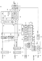
【解決手段】選択トランジスタ903を介して検出ノードAに接続された電気ヒューズ902と、選択トランジスタ903をオフさせた状態で検出ノードAをプリチャージするプリチャージトランジスタ904と、選択トランジスタ903をオンさせ、プリチャージトランジスタ904をオフさせた状態で、検出ノードAにバイアス電流を流すバイアストランジスタ905と、検出ノードAにバイアス電流が流れている状態で検出ノードAの電位を検出する検出回路906とを備え、バイアストランジスタ905は、バイアス電流の量を段階的又は連続的に減少させる。
【選択図】図3
Description
11 アドレス端子
12 コマンド端子
13,14 電源端子
15 リセット端子
16 クロック端子
17 データ入出力端子
21 アドレスバッファ
31 コマンドバッファ
32 コマンドデコーダ
41 入力バッファ
42 DLL回路
51 ロウアドレスラッチ回路
52 カラムアドレスラッチ回路
61 メモリセルアレイ
62 ロウデコーダ
63 カラムデコーダ
64 センス回路
65 冗長メモリセル
66 冗長ロウデコーダ
71 リードライトアンプ
72 入出力バッファ
80 ヒューズ制御回路
90 アンチヒューズ読み出し回路
91 内部電源発生回路
92 アンチヒューズセット
93 ラッチ回路
94 アンチヒューズ回路
95 比較回路
801 制御信号発生部
802 遅延回路
803 バイアス発生回路
901 ドライバ回路
902 アンチヒューズ
903 選択トランジスタ
904 プリチャージトランジスタ
905 バイアストランジスタ
906 検出回路
907 P型トランジスタ
908 N型トランジスタ
909 フィードバックトランジスタ
910 ディスチャージトランジスタ
A 検出ノード
ADD アドレス信号
B,C ノード
BIAS バイアス電圧
BIAS_CONT1,BIAS_CONT2 バイアス制御信号
BL ビット線
CAS カラムアドレスストローブ信号
CK 外部クロック信号
COM コマンド信号
CS チップセレクト信号
DETECT 検知信号
DQ0-n ライト/リードデータ
FLD ヒューズラッチデータ
HIT 一致信号
ICLK,LCLK 内部クロック信号
INV インバータ
MC メモリセル
PREB プリチャージ信号
PROG_A,PROG_B プログラム信号
RAS ロウアドレスストローブ信号
RESETB リセット信号
SA センスアンプ
T1,T2 期間
VDD 電源電圧
VPERI 内部電圧
VSS 接地電位
WE ライトイネーブル信号
WL ワード線
XADD ロウアドレス
YADD カラムアドレス
Claims (8)
- 選択トランジスタを介して検出ノードに接続された電気ヒューズと、
前記選択トランジスタをオフさせた状態で前記検出ノードをプリチャージするプリチャージトランジスタと、
前記選択トランジスタをオンさせ、前記プリチャージトランジスタをオフさせた状態で、前記検出ノードにバイアス電流を流すバイアストランジスタと、
前記検出ノードに前記バイアス電流が流れている状態で前記検出ノードの電位を検出する検出回路と、を備え、
前記バイアストランジスタは、前記バイアス電流の量を段階的又は連続的に減少させることを特徴とする半導体装置。 - 前記検出回路は、前記検出ノードのレベルがしきい値を超えていることに応答して前記バイアストランジスタを活性化させ、前記検出ノードのレベルがしきい値未満であることに応答して前記バイアストランジスタを非活性化させるフィードバックトランジスタを含むことを特徴とする請求項1に記載の半導体装置。
- 前記検出回路は、前記検出ノードのレベルがしきい値未満であることに応答して前記検出ノードをディスチャージするディスチャージトランジスタをさらに含むことを特徴とする請求項2に記載の半導体装置。
- 前記プリチャージトランジスタは、電源ラインと前記検出ノードとの間に接続されており、
前記バイアストランジスタと前記フィードバックトランジスタは、前記電源ラインと前記検出ノードとの間に直列接続されていることを特徴とする請求項2又は3に記載の半導体装置。 - 前記バイアストランジスタは、第1の期間においては前記バイアス電流の量を相対的に大きい第1の電流量とし、前記第1の期間に続く第2の期間においては前記バイアス電流の量を相対的に小さい第2の電流量とし、前記第2の期間は前記第1の期間よりも短いことを特徴とする請求項1乃至4のいずれか一項に記載の半導体装置。
- 第1の期間において、電気ヒューズの一端に第1の電流を供給し、
前記第1の期間の経過後の第2の期間において、前記電気ヒューズの前記一端に前記第1の電流よりも小さい第2の電流を供給し、
前記第1及び第2の期間において前記電気ヒューズがプログラムされているかを前記電気ヒューズの前記一端の電圧を検知して判定することを特徴とする半導体装置の制御方法。 - 前記第1の期間は前記第2の期間よりも長いことを特徴とする請求項6に記載の半導体装置の制御方法。
- 前記第1及び第2の電流はトランジスタにより供給され、前記トランジスタのバイアスを制御することにより生成されることを特徴とする請求項6又は7に記載の半導体装置の制御方法。
Priority Applications (2)
| Application Number | Priority Date | Filing Date | Title |
|---|---|---|---|
| JP2010255526A JP2012109329A (ja) | 2010-11-16 | 2010-11-16 | 半導体装置及びその制御方法 |
| US13/296,437 US9543037B2 (en) | 2010-11-16 | 2011-11-15 | Semiconductor device having electrical fuse and control method thereof |
Applications Claiming Priority (1)
| Application Number | Priority Date | Filing Date | Title |
|---|---|---|---|
| JP2010255526A JP2012109329A (ja) | 2010-11-16 | 2010-11-16 | 半導体装置及びその制御方法 |
Publications (1)
| Publication Number | Publication Date |
|---|---|
| JP2012109329A true JP2012109329A (ja) | 2012-06-07 |
Family
ID=46047658
Family Applications (1)
| Application Number | Title | Priority Date | Filing Date |
|---|---|---|---|
| JP2010255526A Ceased JP2012109329A (ja) | 2010-11-16 | 2010-11-16 | 半導体装置及びその制御方法 |
Country Status (2)
| Country | Link |
|---|---|
| US (1) | US9543037B2 (ja) |
| JP (1) | JP2012109329A (ja) |
Cited By (1)
| Publication number | Priority date | Publication date | Assignee | Title |
|---|---|---|---|---|
| WO2022059176A1 (ja) * | 2020-09-18 | 2022-03-24 | タワー パートナーズ セミコンダクター株式会社 | 半導体装置 |
Families Citing this family (5)
| Publication number | Priority date | Publication date | Assignee | Title |
|---|---|---|---|---|
| US9499428B2 (en) | 2012-07-20 | 2016-11-22 | Ferro Corporation | Formation of glass-based seals using focused infrared radiation |
| US9111624B2 (en) * | 2013-03-22 | 2015-08-18 | Katsuyuki Fujita | Semiconductor memory device |
| US9613714B1 (en) * | 2016-01-19 | 2017-04-04 | Ememory Technology Inc. | One time programming memory cell and memory array for physically unclonable function technology and associated random code generating method |
| US10839934B2 (en) * | 2018-05-30 | 2020-11-17 | Arm Limited | Redundancy circuitry for memory application |
| US20250149101A1 (en) * | 2023-11-06 | 2025-05-08 | Micron Technology, Inc. | Voltage regulation for memory array test procedures |
Citations (7)
| Publication number | Priority date | Publication date | Assignee | Title |
|---|---|---|---|---|
| JP2000500901A (ja) * | 1996-08-01 | 2000-01-25 | マイクロン・テクノロジー・インコーポレーテッド | アンチヒューズ検出回路 |
| JP2000503794A (ja) * | 1996-10-03 | 2000-03-28 | マイクロン・テクノロジー・インコーポレーテッド | アンチヒューズ検出回路 |
| JP2000512059A (ja) * | 1996-10-07 | 2000-09-12 | マイクロン・テクノロジー・インコーポレーテッド | アンチヒューズ用の電荷共有検出回路 |
| JP2009194139A (ja) * | 2008-02-14 | 2009-08-27 | Fujitsu Microelectronics Ltd | 半導体装置及びその制御方法 |
| JP2009259384A (ja) * | 2008-04-16 | 2009-11-05 | Magnachip Semiconductor Ltd | 不揮発性メモリ装置 |
| JP2010109259A (ja) * | 2008-10-31 | 2010-05-13 | Elpida Memory Inc | 半導体装置 |
| JP2010123753A (ja) * | 2008-11-19 | 2010-06-03 | Elpida Memory Inc | 半導体装置、半導体装置におけるアンチヒューズ素子のプログラム方法、及び半導体装置の製造方法 |
Family Cites Families (5)
| Publication number | Priority date | Publication date | Assignee | Title |
|---|---|---|---|---|
| US5680360A (en) * | 1995-06-06 | 1997-10-21 | Integrated Device Technology, Inc. | Circuits for improving the reliablity of antifuses in integrated circuits |
| KR100247937B1 (ko) * | 1997-11-12 | 2000-03-15 | 윤종용 | 퓨징 장치 |
| US6351425B1 (en) * | 2000-12-07 | 2002-02-26 | Micron Technology, Inc. | Method and circuit for high voltage programming of antifuses, and memory device and computer system using same |
| JP4903015B2 (ja) | 2006-06-06 | 2012-03-21 | ルネサスエレクトロニクス株式会社 | 半導体装置、電気ヒューズの切断方法、および電気ヒューズの判定方法 |
| KR100904468B1 (ko) * | 2007-11-28 | 2009-06-24 | 주식회사 하이닉스반도체 | 안티퓨즈 리페어 전압 제어 회로 |
-
2010
- 2010-11-16 JP JP2010255526A patent/JP2012109329A/ja not_active Ceased
-
2011
- 2011-11-15 US US13/296,437 patent/US9543037B2/en active Active
Patent Citations (7)
| Publication number | Priority date | Publication date | Assignee | Title |
|---|---|---|---|---|
| JP2000500901A (ja) * | 1996-08-01 | 2000-01-25 | マイクロン・テクノロジー・インコーポレーテッド | アンチヒューズ検出回路 |
| JP2000503794A (ja) * | 1996-10-03 | 2000-03-28 | マイクロン・テクノロジー・インコーポレーテッド | アンチヒューズ検出回路 |
| JP2000512059A (ja) * | 1996-10-07 | 2000-09-12 | マイクロン・テクノロジー・インコーポレーテッド | アンチヒューズ用の電荷共有検出回路 |
| JP2009194139A (ja) * | 2008-02-14 | 2009-08-27 | Fujitsu Microelectronics Ltd | 半導体装置及びその制御方法 |
| JP2009259384A (ja) * | 2008-04-16 | 2009-11-05 | Magnachip Semiconductor Ltd | 不揮発性メモリ装置 |
| JP2010109259A (ja) * | 2008-10-31 | 2010-05-13 | Elpida Memory Inc | 半導体装置 |
| JP2010123753A (ja) * | 2008-11-19 | 2010-06-03 | Elpida Memory Inc | 半導体装置、半導体装置におけるアンチヒューズ素子のプログラム方法、及び半導体装置の製造方法 |
Cited By (2)
| Publication number | Priority date | Publication date | Assignee | Title |
|---|---|---|---|---|
| WO2022059176A1 (ja) * | 2020-09-18 | 2022-03-24 | タワー パートナーズ セミコンダクター株式会社 | 半導体装置 |
| US12260922B2 (en) | 2020-09-18 | 2025-03-25 | Tower Partners Semiconductor Co., Ltd. | Semiconductor device for writing to a storage element |
Also Published As
| Publication number | Publication date |
|---|---|
| US20120120750A1 (en) | 2012-05-17 |
| US9543037B2 (en) | 2017-01-10 |
Similar Documents
| Publication | Publication Date | Title |
|---|---|---|
| US10665311B2 (en) | Apparatuses and methods including anti-fuses and for reading and programming of same | |
| US8134882B2 (en) | Semiconductor device including an anti-fuse element | |
| US20150043288A1 (en) | Semiconductor memory device having fuse cell array | |
| US9543037B2 (en) | Semiconductor device having electrical fuse and control method thereof | |
| US9418763B2 (en) | Memory array, memory device, and methods for reading and operating the same | |
| US9941870B2 (en) | Adjustable delay circuit for optimizing timing margin | |
| US8422327B2 (en) | Semiconductor device having nonvolatile memory element and manufacturing method thereof | |
| CN110310680B (zh) | 存储器电路及其配置方法、以及从弱单元读取数据的方法 | |
| US8699256B2 (en) | Semiconductor device having nonvolatile memory elements | |
| US20120120735A1 (en) | Semiconductor device having electrical fuse and control method thereof | |
| JP2006236511A (ja) | 半導体集積回路装置 | |
| US9431128B2 (en) | Semiconductor device including fuse circuit | |
| JP2012109403A5 (ja) | ||
| US8023354B2 (en) | Semiconductor memory device including a fuse set and a current controlling unit | |
| JP4922009B2 (ja) | 半導体記憶装置 | |
| JP2010182365A (ja) | アンチヒューズ回路及び半導体記憶装置 | |
| US9378841B2 (en) | Semiconductor fuses and methods of operating the same | |
| US8395439B2 (en) | Semiconductor device having fuse circuit and control method thereof | |
| US8611128B2 (en) | ROM memory device | |
| JP2013016222A (ja) | 半導体装置 | |
| JP2015191677A (ja) | 半導体装置 | |
| JP2000200498A (ja) | 半導体装置 | |
| JP2013020675A (ja) | 半導体装置 | |
| KR101094948B1 (ko) | 반도체 메모리장치 및 이의 백바이어스 전압 설정방법 | |
| JP2015177126A (ja) | 半導体装置 |
Legal Events
| Date | Code | Title | Description |
|---|---|---|---|
| A711 | Notification of change in applicant |
Free format text: JAPANESE INTERMEDIATE CODE: A711 Effective date: 20131029 |
|
| A711 | Notification of change in applicant |
Free format text: JAPANESE INTERMEDIATE CODE: A711 Effective date: 20131030 |
|
| A621 | Written request for application examination |
Free format text: JAPANESE INTERMEDIATE CODE: A621 Effective date: 20131031 |
|
| A977 | Report on retrieval |
Free format text: JAPANESE INTERMEDIATE CODE: A971007 Effective date: 20140620 |
|
| A131 | Notification of reasons for refusal |
Free format text: JAPANESE INTERMEDIATE CODE: A131 Effective date: 20140701 |
|
| A521 | Written amendment |
Free format text: JAPANESE INTERMEDIATE CODE: A523 Effective date: 20140930 |
|
| A01 | Written decision to grant a patent or to grant a registration (utility model) |
Free format text: JAPANESE INTERMEDIATE CODE: A01 Effective date: 20141125 |
|
| A601 | Written request for extension of time |
Free format text: JAPANESE INTERMEDIATE CODE: A601 Effective date: 20141210 |
|
| A602 | Written permission of extension of time |
Free format text: JAPANESE INTERMEDIATE CODE: A602 Effective date: 20141219 |
|
| A045 | Written measure of dismissal of application |
Free format text: JAPANESE INTERMEDIATE CODE: A045 Effective date: 20150324 |