JP2012114445A - 金属ゲート電極を有する半導体素子の製造方法 - Google Patents
金属ゲート電極を有する半導体素子の製造方法 Download PDFInfo
- Publication number
- JP2012114445A JP2012114445A JP2011256006A JP2011256006A JP2012114445A JP 2012114445 A JP2012114445 A JP 2012114445A JP 2011256006 A JP2011256006 A JP 2011256006A JP 2011256006 A JP2011256006 A JP 2011256006A JP 2012114445 A JP2012114445 A JP 2012114445A
- Authority
- JP
- Japan
- Prior art keywords
- film
- region
- groove
- metal
- forming
- Prior art date
- Legal status (The legal status is an assumption and is not a legal conclusion. Google has not performed a legal analysis and makes no representation as to the accuracy of the status listed.)
- Granted
Links
Images








Classifications
-
- H—ELECTRICITY
- H10—SEMICONDUCTOR DEVICES; ELECTRIC SOLID-STATE DEVICES NOT OTHERWISE PROVIDED FOR
- H10D—INORGANIC ELECTRIC SEMICONDUCTOR DEVICES
- H10D84/00—Integrated devices formed in or on semiconductor substrates that comprise only semiconducting layers, e.g. on Si wafers or on GaAs-on-Si wafers
- H10D84/01—Manufacture or treatment
- H10D84/0123—Integrating together multiple components covered by H10D12/00 or H10D30/00, e.g. integrating multiple IGBTs
- H10D84/0126—Integrating together multiple components covered by H10D12/00 or H10D30/00, e.g. integrating multiple IGBTs the components including insulated gates, e.g. IGFETs
- H10D84/0165—Integrating together multiple components covered by H10D12/00 or H10D30/00, e.g. integrating multiple IGBTs the components including insulated gates, e.g. IGFETs the components including complementary IGFETs, e.g. CMOS devices
- H10D84/0172—Manufacturing their gate conductors
- H10D84/0177—Manufacturing their gate conductors the gate conductors having different materials or different implants
-
- H—ELECTRICITY
- H10—SEMICONDUCTOR DEVICES; ELECTRIC SOLID-STATE DEVICES NOT OTHERWISE PROVIDED FOR
- H10P—GENERIC PROCESSES OR APPARATUS FOR THE MANUFACTURE OR TREATMENT OF DEVICES COVERED BY CLASS H10
- H10P50/00—Etching of wafers, substrates or parts of devices
- H10P50/71—Etching of wafers, substrates or parts of devices using masks for conductive or resistive materials
-
- H—ELECTRICITY
- H10—SEMICONDUCTOR DEVICES; ELECTRIC SOLID-STATE DEVICES NOT OTHERWISE PROVIDED FOR
- H10D—INORGANIC ELECTRIC SEMICONDUCTOR DEVICES
- H10D30/00—Field-effect transistors [FET]
- H10D30/60—Insulated-gate field-effect transistors [IGFET]
-
- H—ELECTRICITY
- H10—SEMICONDUCTOR DEVICES; ELECTRIC SOLID-STATE DEVICES NOT OTHERWISE PROVIDED FOR
- H10D—INORGANIC ELECTRIC SEMICONDUCTOR DEVICES
- H10D64/00—Electrodes of devices having potential barriers
- H10D64/01—Manufacture or treatment
- H10D64/013—Manufacture or treatment of electrodes having a conductor capacitively coupled to a semiconductor by an insulator
- H10D64/01302—Manufacture or treatment of electrodes having a conductor capacitively coupled to a semiconductor by an insulator the insulator being formed after the semiconductor body, the semiconductor being silicon
- H10D64/01304—Manufacture or treatment of electrodes having a conductor capacitively coupled to a semiconductor by an insulator the insulator being formed after the semiconductor body, the semiconductor being silicon characterised by the conductor
- H10D64/01318—Manufacture or treatment of electrodes having a conductor capacitively coupled to a semiconductor by an insulator the insulator being formed after the semiconductor body, the semiconductor being silicon characterised by the conductor the conductor comprising a layer of alloy material, compound material or organic material contacting the insulator, e.g. TiN
-
- H—ELECTRICITY
- H10—SEMICONDUCTOR DEVICES; ELECTRIC SOLID-STATE DEVICES NOT OTHERWISE PROVIDED FOR
- H10D—INORGANIC ELECTRIC SEMICONDUCTOR DEVICES
- H10D64/00—Electrodes of devices having potential barriers
- H10D64/01—Manufacture or treatment
- H10D64/017—Manufacture or treatment using dummy gates in processes wherein at least parts of the final gates are self-aligned to the dummy gates, i.e. replacement gate processes
-
- H—ELECTRICITY
- H10—SEMICONDUCTOR DEVICES; ELECTRIC SOLID-STATE DEVICES NOT OTHERWISE PROVIDED FOR
- H10D—INORGANIC ELECTRIC SEMICONDUCTOR DEVICES
- H10D64/00—Electrodes of devices having potential barriers
- H10D64/60—Electrodes characterised by their materials
- H10D64/66—Electrodes having a conductor capacitively coupled to a semiconductor by an insulator, e.g. MIS electrodes
- H10D64/667—Electrodes having a conductor capacitively coupled to a semiconductor by an insulator, e.g. MIS electrodes the conductor comprising a layer of alloy material, compound material or organic material contacting the insulator, e.g. TiN workfunction layers
-
- H—ELECTRICITY
- H10—SEMICONDUCTOR DEVICES; ELECTRIC SOLID-STATE DEVICES NOT OTHERWISE PROVIDED FOR
- H10D—INORGANIC ELECTRIC SEMICONDUCTOR DEVICES
- H10D64/00—Electrodes of devices having potential barriers
- H10D64/60—Electrodes characterised by their materials
- H10D64/66—Electrodes having a conductor capacitively coupled to a semiconductor by an insulator, e.g. MIS electrodes
- H10D64/667—Electrodes having a conductor capacitively coupled to a semiconductor by an insulator, e.g. MIS electrodes the conductor comprising a layer of alloy material, compound material or organic material contacting the insulator, e.g. TiN workfunction layers
- H10D64/669—Electrodes having a conductor capacitively coupled to a semiconductor by an insulator, e.g. MIS electrodes the conductor comprising a layer of alloy material, compound material or organic material contacting the insulator, e.g. TiN workfunction layers the conductor further comprising additional layers of alloy material, compound material or organic material, e.g. TaN/TiAlN
-
- H—ELECTRICITY
- H10—SEMICONDUCTOR DEVICES; ELECTRIC SOLID-STATE DEVICES NOT OTHERWISE PROVIDED FOR
- H10D—INORGANIC ELECTRIC SEMICONDUCTOR DEVICES
- H10D84/00—Integrated devices formed in or on semiconductor substrates that comprise only semiconducting layers, e.g. on Si wafers or on GaAs-on-Si wafers
- H10D84/01—Manufacture or treatment
- H10D84/02—Manufacture or treatment characterised by using material-based technologies
- H10D84/03—Manufacture or treatment characterised by using material-based technologies using Group IV technology, e.g. silicon technology or silicon-carbide [SiC] technology
- H10D84/038—Manufacture or treatment characterised by using material-based technologies using Group IV technology, e.g. silicon technology or silicon-carbide [SiC] technology using silicon technology, e.g. SiGe
Landscapes
- Internal Circuitry In Semiconductor Integrated Circuit Devices (AREA)
- Insulated Gate Type Field-Effect Transistor (AREA)
- Electrodes Of Semiconductors (AREA)
- Metal-Oxide And Bipolar Metal-Oxide Semiconductor Integrated Circuits (AREA)
- Chemical & Material Sciences (AREA)
- Composite Materials (AREA)
- Engineering & Computer Science (AREA)
- Materials Engineering (AREA)
Abstract
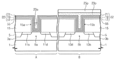
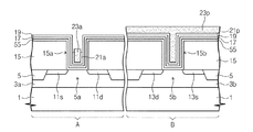
【解決手段】 半導体基板1の上の第1領域A内及び第2領域B内に各々形成された第1グルーブ15a及び第2グルーブ15bを有する層間絶縁膜15を形成する。次に、半導体基板1上に積層金属膜22を形成し、積層金属膜22上に非感光性を有する平坦化膜23を第1グルーブ15a及び第2グルーブ15bを充填するように形成する。第1領域A内の平坦化膜23を乾式エッチングによって選択的に除去し、第1領域A内の積層金属膜22を露出させ、第2領域B内の積層金属膜22を覆う平坦化膜パターン23pを形成する。これにより、第1領域A内の最上部金属膜を容易に除去することができるので、収率が低下することなく異なる仕事関数を有する第1金属ゲート電極及び第2金属ゲート電極を形成できる。
【選択図】 図6
Description
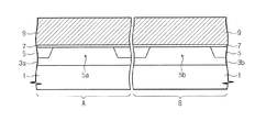
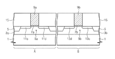
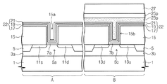
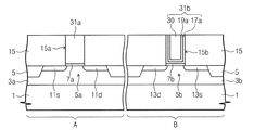
図1から図8までは、本発明の第1実施形態による半導体素子の製造方法を説明するための断面図である。

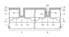
図10から図12までは、本発明の第2実施形態による半導体素子の製造方法を説明するための断面図である。第2実施形態は、ゲート絶縁膜を形成する方法において図1から図9までを参照して説明した第1実施形態と異なる。
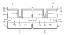
図13から図17までは、本発明の第3実施形態による半導体素子の製造方法を説明するための断面図である。第3実施形態は、金属ゲート電極を形成する方法において、図10から図12までで説明された第2実施形態と異なる。
図18〜図20は、本発明の第4実施形態による半導体素子の製造方法を説明するための断面図である。
5 ・・・素子分離膜、
5a ・・・第1活性領域、
5b ・・・第2活性領域、
7a、55a ・・・第1ゲート絶縁膜、
7b、55b ・・・第2ゲート絶縁膜、
9a ・・・第1ダミーゲート電極、
9b ・・・第2ダミーゲート電極、
15a ・・・第1グルーブ、
15b ・・・第2グルーブ、
15 ・・・層間絶縁膜、
17 ・・・第1金属膜、
19 ・・・第2金属膜、
21 ・・・第3金属膜、
22 ・・・積層金属膜、
23 ・・・平坦化膜、
25 ・・・反射防止膜、
27 ・・・感光膜パターン、
31a ・・・第1金属ゲート電極、
31b ・・・第2金属ゲート電極、
54a ・・・第1ダミーゲートパターン、
54b ・・・第2ダミーゲートパターン。
Claims (17)
- 第1領域及び第2領域を有する半導体基板を準備する段階と、
前記第1領域内及び前記第2領域内に各々配置された第1グルーブ及び第2グルーブを有する層間絶縁膜と、前記第1グルーブ及び前記第2グルーブの少なくとも底面を覆うゲート絶縁膜と、を包含するように前記半導体基板の上に絶縁膜を形成する段階と、
前記絶縁膜を有する基板の全面の上に積層金属膜を形成する段階と、
前記第1グルーブ及び前記第2グルーブを充填するように前記積層金属膜の上に非感光性を有する平坦化膜を形成する段階と、
前記第1領域内の前記平坦化膜を乾式エッチングによって選択的に除去し、前記第1領域内の前記積層金属膜を少なくとも一部露出させ、前記第2領域内の前記積層金属膜を覆う平坦化膜パターンを形成する段階と、
を含む半導体素子の製造方法。 - 前記第1領域はNチャンネルMOSトランジスタ領域を含み、前記第2領域はPチャンネルMOSトランジスタ領域を含むことを特徴とする請求項1に記載の半導体素子の製造方法。
- 前記絶縁膜を形成する段階は、
前記第1領域及び前記第2領域を有する前記半導体基板の上にゲート絶縁膜及びダミー導電膜を順に形成する段階と、
前記ダミー導電膜及び前記ゲート絶縁膜をパターニングして、前記第1領域内に順に積層された第1ゲート絶縁膜及び第1ダミーゲート電極と、前記第2領域内に順に積層された第2ゲート絶縁膜及び第2ダミーゲート電極と、を形成する段階と、
前記第1ダミーゲート電極及び前記第2ダミーゲート電極を有する基板の全面の上に前記層間絶縁膜を形成する段階と、
前記層間絶縁膜を平坦化させて前記第1ダミーゲート電極及び前記第2ダミーゲート電極を露出させる段階と、
露出させた前記第1ダミーゲート電極及び前記第2ダミーゲート電極を除去して前記第1ゲート絶縁膜及び前記第2ゲート絶縁膜を各々露出させる前記第1グルーブ及び前記第2グルーブを形成する段階と、
を含むことを特徴とする請求項1に記載の半導体素子の製造方法。 - 前記絶縁膜を形成する段階は、
前記第1領域及び前記第2領域を有する前記半導体基板の上にダミー物質膜を形成する段階と、
前記ダミー物質膜をパターニングして前記第1領域内及び前記第2領域内に各々第1ダミーゲートパターン及び第2ダミーゲートパターンを形成する段階と、
前記第1ダミーゲートパターン及び前記第2ダミーゲートパターンを有する基板の上に前記層間絶縁膜を形成する段階と、
前記層間絶縁膜を平坦化させて前記第1ダミーゲートパターン及び前記第2ダミーゲートパターンを露出させる段階と、
露出させた前記第1ダミーゲートパターン及び前記第2ダミーゲートパターンを除去して前記第1領域内及び前記第2領域内に各々前記第1グルーブ及び前記第2グルーブを形成する段階と、
前記第1グルーブ及び前記第2グルーブを有する基板の全面の上に同じ厚さのゲート絶縁膜を形成する段階と、
を含み、
前記積層金属膜は前記ゲート絶縁膜の上に形成されることを特徴とする請求項1に記載の半導体素子の製造方法。 - 前記平坦化膜は、SOH(spin on hardmask)膜又は非晶質炭素膜(amorphous carbon layer;ACL)から形成され、
前記第1領域内の前記平坦化膜を乾式エッチングする段階は、酸素ガス及び窒素ガスを含むプロセスガスを使用することを特徴とする請求項1に記載の半導体素子の製造方法。 - 前記プロセスガスは、アルゴンガスをさらに含むことを特徴とする請求項5に記載の半導体素子の製造方法。
- 前記SOH膜は、炭素含有SOH膜、又はシリコン含有SOH膜から形成されることを特徴とする請求項5に記載の半導体素子の製造方法。
- 前記SOH膜を形成する段階は、
前記積層金属膜の上に樹脂溶液を塗布して前記第1グルーブ及び前記第2グルーブを満たす段階と、
前記樹脂溶液をベークして熱硬化された樹脂膜(cured resin layer)を形成する段階と、
を含むことを特徴とする請求項7に記載の半導体素子の製造方法。 - 前記平坦化膜パターンを形成する段階は、
前記平坦化膜の上に前記第1領域内の前記平坦化膜を露出させる無機反射防止膜パターンを形成する段階と、
前記無機反射防止膜パターンをエッチングマスクとして露出させた前記平坦化膜を乾式エッチングする段階と、
前記無機反射防止膜パターンを除去する段階と、
を含むことを特徴とする請求項1に記載の半導体素子の製造方法。 - 前記無機反射防止膜パターンを形成する段階は、
前記平坦化膜の上に無機反射防止膜(inorganic anti−reflective layer)を形成する段階と、
前記無機反射防止膜の上に前記第2領域を覆う感光膜パターンを形成する段階と、
前記第1領域内の前記無機反射防止膜を乾式エッチングして前記第1領域内の前記平坦化膜を選択的に露出させる段階と、
前記感光膜パターンを除去する段階と、
を含むことを特徴とする請求項9に記載の半導体素子の製造方法。 - 前記積層金属膜を形成する段階は、
第1金属膜、第2金属膜、及び第3金属膜を順に形成する段階を含むことを特徴とする請求項1に記載の半導体素子の製造方法。 - 前記第1金属膜、前記第2金属膜、及び前記第3金属膜は、各々下部窒化チタンTiN、窒化タンタルTaN、及び上部窒化チタンTiNから形成されることを特徴とする請求項11に記載の半導体素子の製造方法。
- 前記平坦化膜パターンをエッチングマスクとして前記第1領域内の前記積層金属膜の最上部金属膜を除去する段階と、
前記平坦化膜パターンを除去する段階と、
前記平坦化膜パターンが除去された結果物全面の上に前記第1グルーブ及び前記第2グルーブを充填するキャッピング金属膜を形成する段階と、
前記層間絶縁膜の上面が露出するまで前記キャッピング金属膜及び前記積層金属膜を平坦化させて前記第1グルーブ内及び前記第2グルーブ内に各々第1金属ゲート電極及び第2金属ゲート電極を形成する段階と、
をさらに含むことを特徴とする請求項1に記載の半導体素子の製造方法。 - 前記平坦化膜パターンは、N2H2ガスをプロセスガスとするアッシング工程によって除去されることを特徴とする請求項13に記載の半導体素子の製造方法。
- 前記キャッピング金属膜は、アルミニウム合金から形成されることを特徴とする請求項13に記載の半導体素子の製造方法。
- 第1領域及び第2領域を有する半導体基板を準備する段階と、
前記第1領域内及び前記第2領域内に各々配置された第1グルーブ及び第2グルーブを有する層間絶縁膜と前記第1グルーブ及び前記第2グルーブの少なくとも底面を覆うゲート絶縁膜とを包含するように前記半導体基板の上に絶縁膜を形成する段階と、
前記絶縁膜を有する基板の全面の上に積層金属膜を形成する段階と、
前記積層金属膜の上に非感光性を有する平坦化膜を形成し、前記平坦化膜は前記第1グルーブ及び第2グルーブを充填するように形成される段階と、
前記第1領域内の前記平坦化膜を乾式エッチングによって部分エッチングすることにより前記第1グルーブ内に残る第1平坦化膜残余物、及び前記第2領域を覆う平坦化膜パターンを形成する段階と、
を含むことを特徴とする半導体素子の製造方法。 - 第1領域と第2領域とを含む半導体基板を準備する段階と、
第1グルーブと第2グルーブとを有する絶縁膜を形成する段階と、
前記絶縁膜の上に複数の金属膜を有する積層金属膜を形成する段階と、
前記第1領域の前記積層金属膜の複数の金属膜から第1数の金属膜を有し、第2領域の前記積層金属膜の複数の金属膜から第2数の金属膜を有するように前記積層金属膜を処理する段階と、
前記第1領域の前記第1数の金属膜の上及び前記第2領域で前記第2数の金属膜の上にキャッピング金属膜を形成する段階と、
前記キャッピング金属膜を平坦化して前記第1領域の前記第1グルーブ内で前記第1数の金属膜から第1金属ゲート電極を形成し、前記第2領域の前記第2グルーブ内で前記第2数の金属膜から第2金属ゲート電極を形成する段階と、
を含むことを特徴とする半導体装置の製造方法。
Applications Claiming Priority (2)
| Application Number | Priority Date | Filing Date | Title |
|---|---|---|---|
| KR1020100117666A KR101746709B1 (ko) | 2010-11-24 | 2010-11-24 | 금속 게이트 전극들을 갖는 반도체 소자의 제조방법 |
| KR10-2010-0117666 | 2010-11-24 |
Publications (2)
| Publication Number | Publication Date |
|---|---|
| JP2012114445A true JP2012114445A (ja) | 2012-06-14 |
| JP5917893B2 JP5917893B2 (ja) | 2016-05-18 |
Family
ID=46021446
Family Applications (1)
| Application Number | Title | Priority Date | Filing Date |
|---|---|---|---|
| JP2011256006A Active JP5917893B2 (ja) | 2010-11-24 | 2011-11-24 | 金属ゲート電極を有する半導体素子の製造方法 |
Country Status (5)
| Country | Link |
|---|---|
| US (1) | US8946026B2 (ja) |
| JP (1) | JP5917893B2 (ja) |
| KR (1) | KR101746709B1 (ja) |
| CN (1) | CN102543876B (ja) |
| DE (1) | DE102011054757B9 (ja) |
Cited By (1)
| Publication number | Priority date | Publication date | Assignee | Title |
|---|---|---|---|---|
| CN105374857A (zh) * | 2014-08-26 | 2016-03-02 | 中芯国际集成电路制造(上海)有限公司 | 金属栅极结构及其形成方法 |
Families Citing this family (24)
| Publication number | Priority date | Publication date | Assignee | Title |
|---|---|---|---|---|
| US9337110B2 (en) * | 2011-10-19 | 2016-05-10 | Taiwan Semiconductor Manufacturing Company, Ltd. | Semiconductor device having metal gate electrode and method of fabrication thereof |
| US8951855B2 (en) * | 2012-04-24 | 2015-02-10 | United Microelectronics Corp. | Manufacturing method for semiconductor device having metal gate |
| US8999829B2 (en) * | 2012-10-19 | 2015-04-07 | Applied Materials, Inc. | Dual gate process |
| KR101996244B1 (ko) | 2013-06-27 | 2019-07-05 | 삼성전자 주식회사 | 반도체 소자 제조 방법 |
| US9281201B2 (en) * | 2013-09-18 | 2016-03-08 | United Microelectronics Corp. | Method of manufacturing semiconductor device having metal gate |
| EP3832710B1 (en) | 2013-09-27 | 2024-01-10 | INTEL Corporation | Non-planar i/o and logic semiconductor devices having different workfunction on common substrate |
| CN104681489A (zh) * | 2013-11-26 | 2015-06-03 | 中芯国际集成电路制造(上海)有限公司 | Cmos晶体管的形成方法 |
| KR102125749B1 (ko) | 2013-12-27 | 2020-07-09 | 삼성전자 주식회사 | 반도체 장치 및 이의 제조 방법 |
| US9231071B2 (en) * | 2014-02-24 | 2016-01-05 | United Microelectronics Corp. | Semiconductor structure and manufacturing method of the same |
| FR3018627A1 (fr) | 2014-03-14 | 2015-09-18 | St Microelectronics Crolles 2 | Procede de formation de regions metalliques de grilles differentes de transistors mos |
| KR102229018B1 (ko) * | 2014-06-02 | 2021-03-17 | 엘지이노텍 주식회사 | 정전기 방지를 위한 정전기 방지 전극이 배선된 터치 패널 |
| KR102312262B1 (ko) * | 2014-09-02 | 2021-10-15 | 삼성전자주식회사 | 반도체 장치 및 이의 제조 방법 |
| US20160086805A1 (en) * | 2014-09-24 | 2016-03-24 | Qualcomm Incorporated | Metal-gate with an amorphous metal layer |
| KR20160148795A (ko) * | 2015-06-16 | 2016-12-27 | 삼성전자주식회사 | 반도체 소자 및 이의 제조 방법 |
| KR102286112B1 (ko) | 2015-10-21 | 2021-08-04 | 삼성전자주식회사 | 반도체 장치 및 이의 제조 방법 |
| US9748350B2 (en) * | 2015-10-30 | 2017-08-29 | Taiwan Semiconductor Manufacturing Co., Ltd. | Semiconductor structure with enlarged gate electrode structure and method for forming the same |
| US9865703B2 (en) * | 2015-12-31 | 2018-01-09 | International Business Machines Corporation | High-K layer chamfering to prevent oxygen ingress in replacement metal gate (RMG) process |
| KR102413039B1 (ko) * | 2016-02-29 | 2022-06-23 | 도쿄엘렉트론가부시키가이샤 | 선택적 SiARC 제거 |
| CN106783740B (zh) * | 2016-12-16 | 2019-11-08 | 上海华力微电子有限公司 | 用于金属栅极的制造技术 |
| CN111162447B (zh) * | 2019-12-31 | 2021-06-15 | 苏州辰睿光电有限公司 | 一种电极窗口、具有电极窗口的半导体器件的制作方法 |
| CN113496878A (zh) * | 2020-04-01 | 2021-10-12 | 中芯国际集成电路制造(上海)有限公司 | 图案化掩膜层的形成方法 |
| US11848239B2 (en) * | 2020-07-10 | 2023-12-19 | Taiwan Semiconductor Manufacturing Co., Ltd. | Patterning method and structures resulting therefrom |
| CN115332076B (zh) * | 2022-07-05 | 2025-06-17 | 福建省晋华集成电路有限公司 | 半导体器件及制备方法 |
| CN115954270A (zh) * | 2023-01-03 | 2023-04-11 | 杭州富芯半导体有限公司 | 一种半导体器件的制备方法 |
Citations (14)
| Publication number | Priority date | Publication date | Assignee | Title |
|---|---|---|---|---|
| JPH04170027A (ja) * | 1990-11-02 | 1992-06-17 | Sony Corp | ドライエッチング方法 |
| JPH10233452A (ja) * | 1997-02-21 | 1998-09-02 | Sony Corp | 金属プラグおよび金属配線の形成方法 |
| JP2003158181A (ja) * | 2001-09-28 | 2003-05-30 | Hynix Semiconductor Inc | 半導体素子の製造方法 |
| JP2005512326A (ja) * | 2001-11-30 | 2005-04-28 | フリースケール セミコンダクター インコーポレイテッド | 非平坦性の影響を最小限にするトランジスタ金属ゲート構造および製造方法 |
| JP2005191567A (ja) * | 2003-12-24 | 2005-07-14 | Hynix Semiconductor Inc | 半導体素子のコンタクト形成方法 |
| JP2005317803A (ja) * | 2004-04-28 | 2005-11-10 | Sharp Corp | 半導体装置の製造方法および半導体装置 |
| JP2007036267A (ja) * | 2006-09-04 | 2007-02-08 | Elpida Memory Inc | Sog膜の形成方法 |
| JP2008016538A (ja) * | 2006-07-04 | 2008-01-24 | Renesas Technology Corp | Mos構造を有する半導体装置及びその製造方法 |
| JP2008066551A (ja) * | 2006-09-08 | 2008-03-21 | Fujitsu Ltd | 半導体装置の製造方法 |
| JP2008523591A (ja) * | 2004-12-07 | 2008-07-03 | インテル コーポレイション | 高誘電率ゲート誘電体および金属ゲート電極をもつ半導体デバイスの作成方法 |
| US20090042405A1 (en) * | 2004-09-08 | 2009-02-12 | Doczy Mark L | Method for making a semiconductor device having a high-k gate dielectric layer and a metal gate electrode |
| US20100068875A1 (en) * | 2008-09-15 | 2010-03-18 | Taiwan Semiconductor Manufacturing Company, Ltd. | Double treatment on hard mask for gate n/p patterning |
| US7732344B1 (en) * | 2009-06-05 | 2010-06-08 | Taiwan Semiconductor Manufacturing Company, Ltd. | High selectivity etching process for metal gate N/P patterning |
| US20110248359A1 (en) * | 2010-04-13 | 2011-10-13 | Guang-Yaw Hwang | Semiconductor device having metal gate and manufacturing method thereof |
Family Cites Families (10)
| Publication number | Priority date | Publication date | Assignee | Title |
|---|---|---|---|---|
| US6087231A (en) * | 1999-08-05 | 2000-07-11 | Advanced Micro Devices, Inc. | Fabrication of dual gates of field transistors with prevention of reaction between the gate electrode and the gate dielectric with a high dielectric constant |
| US6873048B2 (en) | 2003-02-27 | 2005-03-29 | Sharp Laboratories Of America, Inc. | System and method for integrating multiple metal gates for CMOS applications |
| KR100704475B1 (ko) * | 2005-12-28 | 2007-04-09 | 주식회사 하이닉스반도체 | 듀얼 폴리 리세스 게이트를 갖는 반도체 소자의 제조방법 |
| JP2009033032A (ja) | 2007-07-30 | 2009-02-12 | Sony Corp | 半導体装置及び半導体装置の製造方法 |
| US8536660B2 (en) * | 2008-03-12 | 2013-09-17 | Taiwan Semiconductor Manufacturing Company, Ltd. | Hybrid process for forming metal gates of MOS devices |
| US7888195B2 (en) * | 2008-08-26 | 2011-02-15 | United Microelectronics Corp. | Metal gate transistor and method for fabricating the same |
| US7871915B2 (en) | 2008-09-26 | 2011-01-18 | Taiwan Semiconductor Manufacturing Company, Ltd. | Method for forming metal gates in a gate last process |
| KR101532012B1 (ko) * | 2008-12-24 | 2015-06-30 | 삼성전자주식회사 | 반도체 소자 및 반도체 소자의 패턴 형성 방법 |
| US8227890B2 (en) * | 2009-12-18 | 2012-07-24 | United Microelectronics Corporation | Method of forming an electrical fuse and a metal gate transistor and the related electrical fuse |
| US8048810B2 (en) * | 2010-01-29 | 2011-11-01 | Taiwan Semiconductor Manufacturing Company, Ltd. | Method for metal gate N/P patterning |
-
2010
- 2010-11-24 KR KR1020100117666A patent/KR101746709B1/ko active Active
-
2011
- 2011-09-21 US US13/238,284 patent/US8946026B2/en active Active
- 2011-10-24 DE DE102011054757.6A patent/DE102011054757B9/de active Active
- 2011-11-23 CN CN201110375613.XA patent/CN102543876B/zh active Active
- 2011-11-24 JP JP2011256006A patent/JP5917893B2/ja active Active
Patent Citations (14)
| Publication number | Priority date | Publication date | Assignee | Title |
|---|---|---|---|---|
| JPH04170027A (ja) * | 1990-11-02 | 1992-06-17 | Sony Corp | ドライエッチング方法 |
| JPH10233452A (ja) * | 1997-02-21 | 1998-09-02 | Sony Corp | 金属プラグおよび金属配線の形成方法 |
| JP2003158181A (ja) * | 2001-09-28 | 2003-05-30 | Hynix Semiconductor Inc | 半導体素子の製造方法 |
| JP2005512326A (ja) * | 2001-11-30 | 2005-04-28 | フリースケール セミコンダクター インコーポレイテッド | 非平坦性の影響を最小限にするトランジスタ金属ゲート構造および製造方法 |
| JP2005191567A (ja) * | 2003-12-24 | 2005-07-14 | Hynix Semiconductor Inc | 半導体素子のコンタクト形成方法 |
| JP2005317803A (ja) * | 2004-04-28 | 2005-11-10 | Sharp Corp | 半導体装置の製造方法および半導体装置 |
| US20090042405A1 (en) * | 2004-09-08 | 2009-02-12 | Doczy Mark L | Method for making a semiconductor device having a high-k gate dielectric layer and a metal gate electrode |
| JP2008523591A (ja) * | 2004-12-07 | 2008-07-03 | インテル コーポレイション | 高誘電率ゲート誘電体および金属ゲート電極をもつ半導体デバイスの作成方法 |
| JP2008016538A (ja) * | 2006-07-04 | 2008-01-24 | Renesas Technology Corp | Mos構造を有する半導体装置及びその製造方法 |
| JP2007036267A (ja) * | 2006-09-04 | 2007-02-08 | Elpida Memory Inc | Sog膜の形成方法 |
| JP2008066551A (ja) * | 2006-09-08 | 2008-03-21 | Fujitsu Ltd | 半導体装置の製造方法 |
| US20100068875A1 (en) * | 2008-09-15 | 2010-03-18 | Taiwan Semiconductor Manufacturing Company, Ltd. | Double treatment on hard mask for gate n/p patterning |
| US7732344B1 (en) * | 2009-06-05 | 2010-06-08 | Taiwan Semiconductor Manufacturing Company, Ltd. | High selectivity etching process for metal gate N/P patterning |
| US20110248359A1 (en) * | 2010-04-13 | 2011-10-13 | Guang-Yaw Hwang | Semiconductor device having metal gate and manufacturing method thereof |
Cited By (2)
| Publication number | Priority date | Publication date | Assignee | Title |
|---|---|---|---|---|
| CN105374857A (zh) * | 2014-08-26 | 2016-03-02 | 中芯国际集成电路制造(上海)有限公司 | 金属栅极结构及其形成方法 |
| CN105374857B (zh) * | 2014-08-26 | 2018-07-10 | 中芯国际集成电路制造(上海)有限公司 | 金属栅极结构及其形成方法 |
Also Published As
| Publication number | Publication date |
|---|---|
| US8946026B2 (en) | 2015-02-03 |
| JP5917893B2 (ja) | 2016-05-18 |
| DE102011054757B9 (de) | 2022-01-13 |
| DE102011054757B4 (de) | 2021-11-18 |
| CN102543876A (zh) | 2012-07-04 |
| KR101746709B1 (ko) | 2017-06-14 |
| US20120129331A1 (en) | 2012-05-24 |
| CN102543876B (zh) | 2016-01-20 |
| KR20120056112A (ko) | 2012-06-01 |
| DE102011054757A1 (de) | 2012-05-24 |
Similar Documents
| Publication | Publication Date | Title |
|---|---|---|
| JP5917893B2 (ja) | 金属ゲート電極を有する半導体素子の製造方法 | |
| TWI655680B (zh) | 半導體裝置及其形成方法 | |
| TWI671903B (zh) | 半導體裝置結構及其製造方法 | |
| TWI582990B (zh) | 鰭式場效電晶體之源極/汲極區域及其形成方法 | |
| TWI419264B (zh) | 製造半導體裝置的方法 | |
| TW202017189A (zh) | 半導體裝置 | |
| US9105694B2 (en) | Method for fabricating semiconductor device | |
| CN102903742A (zh) | 场效应晶体管的金属栅电极 | |
| TW201448054A (zh) | 製造半導體元件的方法 | |
| US20170256459A1 (en) | Method of fabricating semiconductor structure with self-aligned spacers | |
| CN105321883A (zh) | 制造半导体器件的方法 | |
| CN106952874A (zh) | 多阈值电压鳍式晶体管的形成方法 | |
| TW201730925A (zh) | 半導體結構及其製造方法 | |
| CN106935495A (zh) | 半导体元件的制造方法 | |
| TWI720260B (zh) | 半導體元件及其形成方法 | |
| TW202329253A (zh) | 半導體裝置的形成方法 | |
| KR20160054830A (ko) | 반도체 소자의 제조 방법 | |
| KR102224831B1 (ko) | 반도체 FinFET 디바이스 및 방법 | |
| CN106856189B (zh) | 浅沟槽隔离结构及其形成方法 | |
| TWI848705B (zh) | 半導體裝置的製造方法 | |
| CN104241359A (zh) | 半导体结构及其制作方法 | |
| TWI705526B (zh) | 半導體元件的製造方法 | |
| CN107045981A (zh) | 半导体结构的形成方法 | |
| TW202243006A (zh) | 半導體結構的形成方法 | |
| TWI822111B (zh) | 半導體裝置與其形成方法 |
Legal Events
| Date | Code | Title | Description |
|---|---|---|---|
| A621 | Written request for application examination |
Free format text: JAPANESE INTERMEDIATE CODE: A621 Effective date: 20141016 |
|
| A131 | Notification of reasons for refusal |
Free format text: JAPANESE INTERMEDIATE CODE: A131 Effective date: 20150514 |
|
| A977 | Report on retrieval |
Free format text: JAPANESE INTERMEDIATE CODE: A971007 Effective date: 20150514 |
|
| A521 | Request for written amendment filed |
Free format text: JAPANESE INTERMEDIATE CODE: A523 Effective date: 20150813 |
|
| TRDD | Decision of grant or rejection written | ||
| A01 | Written decision to grant a patent or to grant a registration (utility model) |
Free format text: JAPANESE INTERMEDIATE CODE: A01 Effective date: 20160315 |
|
| A61 | First payment of annual fees (during grant procedure) |
Free format text: JAPANESE INTERMEDIATE CODE: A61 Effective date: 20160407 |
|
| R150 | Certificate of patent or registration of utility model |
Ref document number: 5917893 Country of ref document: JP Free format text: JAPANESE INTERMEDIATE CODE: R150 |
|
| R250 | Receipt of annual fees |
Free format text: JAPANESE INTERMEDIATE CODE: R250 |
|
| R250 | Receipt of annual fees |
Free format text: JAPANESE INTERMEDIATE CODE: R250 |
|
| R250 | Receipt of annual fees |
Free format text: JAPANESE INTERMEDIATE CODE: R250 |
|
| R250 | Receipt of annual fees |
Free format text: JAPANESE INTERMEDIATE CODE: R250 |
|
| R250 | Receipt of annual fees |
Free format text: JAPANESE INTERMEDIATE CODE: R250 |
|
| R250 | Receipt of annual fees |
Free format text: JAPANESE INTERMEDIATE CODE: R250 |
|
| R250 | Receipt of annual fees |
Free format text: JAPANESE INTERMEDIATE CODE: R250 |
|
| R250 | Receipt of annual fees |
Free format text: JAPANESE INTERMEDIATE CODE: R250 |