JP2012146998A - 半導体装置 - Google Patents
半導体装置 Download PDFInfo
- Publication number
- JP2012146998A JP2012146998A JP2012054355A JP2012054355A JP2012146998A JP 2012146998 A JP2012146998 A JP 2012146998A JP 2012054355 A JP2012054355 A JP 2012054355A JP 2012054355 A JP2012054355 A JP 2012054355A JP 2012146998 A JP2012146998 A JP 2012146998A
- Authority
- JP
- Japan
- Prior art keywords
- gate
- semiconductor chip
- lead
- sealing body
- source
- Prior art date
- Legal status (The legal status is an assumption and is not a legal conclusion. Google has not performed a legal analysis and makes no representation as to the accuracy of the status listed.)
- Granted
Links
Images


Classifications
-
- H—ELECTRICITY
- H10—SEMICONDUCTOR DEVICES; ELECTRIC SOLID-STATE DEVICES NOT OTHERWISE PROVIDED FOR
- H10W—GENERIC PACKAGES, INTERCONNECTIONS, CONNECTORS OR OTHER CONSTRUCTIONAL DETAILS OF DEVICES COVERED BY CLASS H10
- H10W72/00—Interconnections or connectors in packages
- H10W72/50—Bond wires
- H10W72/541—Dispositions of bond wires
- H10W72/547—Dispositions of multiple bond wires
- H10W72/5475—Dispositions of multiple bond wires multiple bond wires connected to common bond pads at both ends of the wires
-
- H—ELECTRICITY
- H10—SEMICONDUCTOR DEVICES; ELECTRIC SOLID-STATE DEVICES NOT OTHERWISE PROVIDED FOR
- H10W—GENERIC PACKAGES, INTERCONNECTIONS, CONNECTORS OR OTHER CONSTRUCTIONAL DETAILS OF DEVICES COVERED BY CLASS H10
- H10W72/00—Interconnections or connectors in packages
- H10W72/90—Bond pads, in general
- H10W72/921—Structures or relative sizes of bond pads
- H10W72/926—Multiple bond pads having different sizes
-
- H—ELECTRICITY
- H10—SEMICONDUCTOR DEVICES; ELECTRIC SOLID-STATE DEVICES NOT OTHERWISE PROVIDED FOR
- H10W—GENERIC PACKAGES, INTERCONNECTIONS, CONNECTORS OR OTHER CONSTRUCTIONAL DETAILS OF DEVICES COVERED BY CLASS H10
- H10W90/00—Package configurations
- H10W90/701—Package configurations characterised by the relative positions of pads or connectors relative to package parts
- H10W90/751—Package configurations characterised by the relative positions of pads or connectors relative to package parts of bond wires
- H10W90/756—Package configurations characterised by the relative positions of pads or connectors relative to package parts of bond wires between a chip and a stacked lead frame, conducting package substrate or heat sink
Landscapes
- Internal Circuitry In Semiconductor Integrated Circuit Devices (AREA)
- Lead Frames For Integrated Circuits (AREA)
- Electrodes Of Semiconductors (AREA)
Abstract
【解決手段】 封止体と、前記封止体内に位置する半導体チップと、前記封止体の内外に亘って延在する複数のリードと、前記半導体チップの電極と前記封止体内に位置するリードの内端を電気的に接続する導電性のワイヤとを有し、前記半導体チップには縦型電界効果トランジスタセルが並列接続状態で複数組み込まれ、半導体チップの表面にはゲート電極とソース電極が交互に並んでそれぞれ複数配置されるとともに、前記各電極に対応してリードが並び、前記各電極と前記対応した各リードは前記ワイヤによって接続されていることを特徴とする半導体装置。
【選択図】図11
Description
一方、特開2000-69766号公報には、コンバータやインバータにおけるスイッチング損失を低減する技術が開示されている。この文献には、例えば、インバータとコンデンサを平行平板を用い、相互インダクタンスの効果によって配線の低インダクタンス化を図る技術が開示されている。即ち、この技術はコンバータやインバータの半導体素子外の回路部配線の低インダクタンス化の技術であり、MOSFET内部の低インダクタンス化については記載されていない。
(1)オン抵抗及びスイッチング損失の低減を図ることができる高速駆動が可能な縦型構造のトランジスタを有する半導体装置を提供することができる。
(実施形態1)
本実施形態1では縦型絶縁ゲート電界効果トランジスタ(縦型高耐圧MOSFET)に本発明を適用した例について説明する。
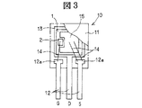
本実施形態1の半導体装置10は、図3に示すような外観形状をしている。図3は本実施形態1の半導体装置の一部を切り欠いた状態の平面図である。絶縁性樹脂で形成される封止体(パッケージ)11の一端から3本のリード12が並んで突出している。中央のリード12がドレインリード(D)となり、左側のリード12がゲートリード(G)となり、右側のリード12がソースリード(S)となっている。
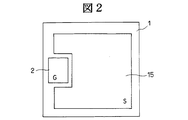
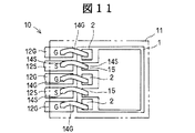
図11は本発明の他の実施形態(実施形態2)である半導体装置10の一部を示す模式的平面図である。本実施形態2では、ゲートワイヤ14Gとソースワイヤ14Sが交互に配置されるように半導体チップ1におけるゲート用ワイヤボンディングパッド2とソース用ワイヤボンディングパッド15が選択的に配置されるとともに、これに対応してゲートリード12Gとソースリード12Sも交互に配置されている。そしてゲートリード12Gの先端延長上にゲート用ワイヤボンディングパッド2が位置し、ソースリード12Sの先端延長上にソース用ワイヤボンディングパッド15が位置し、それぞれゲートワイヤ14G及びソースワイヤ14Sで電気的に接続されている。
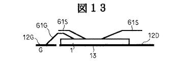
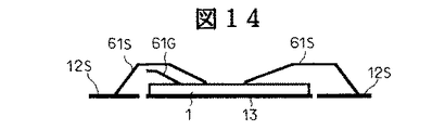
図12乃至図14は本発明の他の実施形態(実施形態3)である半導体装置に係わる図である。図12は半導体装置の一部を示す模式的平面図、図13は図12のA−A線に沿う断面図、図14は図12のB−B線に沿う断面図である。
Claims (2)
- 封止体と、前記封止体内に位置する半導体チップと、前記封止体の内外に亘って延在する複数のリードと、前記半導体チップの電極と前記封止体内に位置するリードの内端を電気的に接続する導電性のワイヤとを有し、前記半導体チップには縦型電界効果トランジスタセルが並列接続状態で複数組み込まれ、半導体チップの表面にはゲート電極とソース電極が交互に並んでそれぞれ複数配置されるとともに、前記各電極に対応してリードが並び、前記各電極と前記対応した各リードは前記ワイヤによって接続されていることを特徴とする半導体装置。
- 封止体と、前記封止体内に位置する半導体チップと、前記封止体の内外に亘って延在する複数のリードと、前記半導体チップの電極と前記封止体内に位置するリードの内端を電気的に接続する導電性の金属板とを有し、前記半導体チップには縦型電界効果トランジスタセルが並列接続状態で複数組み込まれ、半導体チップの表面にはゲート電極及びソース電極並びにドレイン電極が配置され、前記半導体チップの一端側にはソースリードとドレインリードが並ぶとともに他端側にはソースリードとゲートリードが並び、前記一端側のソースリード及びドレインリードにそれぞれ接続される前記金属板は相互に一部で所定の間隔を隔てて重なり、前記他端側のソースリード及びゲートリードにそれぞれ接続される前記金属板は相互に一部で所定の間隔を隔てて重なるように構成されていることを特徴とする半導体装置。
Priority Applications (1)
| Application Number | Priority Date | Filing Date | Title |
|---|---|---|---|
| JP2012054355A JP5448110B2 (ja) | 2012-03-12 | 2012-03-12 | 半導体装置 |
Applications Claiming Priority (1)
| Application Number | Priority Date | Filing Date | Title |
|---|---|---|---|
| JP2012054355A JP5448110B2 (ja) | 2012-03-12 | 2012-03-12 | 半導体装置 |
Related Parent Applications (1)
| Application Number | Title | Priority Date | Filing Date |
|---|---|---|---|
| JP2001201804A Division JP4993824B2 (ja) | 2001-07-03 | 2001-07-03 | 半導体装置 |
Publications (2)
| Publication Number | Publication Date |
|---|---|
| JP2012146998A true JP2012146998A (ja) | 2012-08-02 |
| JP5448110B2 JP5448110B2 (ja) | 2014-03-19 |
Family
ID=46790195
Family Applications (1)
| Application Number | Title | Priority Date | Filing Date |
|---|---|---|---|
| JP2012054355A Expired - Fee Related JP5448110B2 (ja) | 2012-03-12 | 2012-03-12 | 半導体装置 |
Country Status (1)
| Country | Link |
|---|---|
| JP (1) | JP5448110B2 (ja) |
Cited By (3)
| Publication number | Priority date | Publication date | Assignee | Title |
|---|---|---|---|---|
| JP2015153988A (ja) * | 2014-02-18 | 2015-08-24 | 新日本無線株式会社 | 半導体装置 |
| JP2018198316A (ja) * | 2017-05-15 | 2018-12-13 | インフィネオン テクノロジーズ アーゲーInfineon Technologies Ag | ボンドパッド間のゲートフィンガを含むワイドバンドギャップ半導体デバイス |
| WO2024034359A1 (ja) * | 2022-08-10 | 2024-02-15 | ローム株式会社 | 半導体装置 |
Citations (5)
| Publication number | Priority date | Publication date | Assignee | Title |
|---|---|---|---|---|
| JPS5710748U (ja) * | 1980-06-18 | 1982-01-20 | ||
| JPH07235635A (ja) * | 1994-02-14 | 1995-09-05 | Delco Electron Corp | 直線型デュアル・スイッチ・モジュール |
| JPH08213614A (ja) * | 1994-08-02 | 1996-08-20 | Sgs Thomson Microelectron Srl | Mos技術電力デバイスチィップ及びパッケージ組立体 |
| JPH10261756A (ja) * | 1997-03-19 | 1998-09-29 | Hitachi Ltd | 半導体装置およびその製造方法 |
| JPH11111977A (ja) * | 1997-09-30 | 1999-04-23 | Sanyo Electric Co Ltd | 半導体装置 |
-
2012
- 2012-03-12 JP JP2012054355A patent/JP5448110B2/ja not_active Expired - Fee Related
Patent Citations (5)
| Publication number | Priority date | Publication date | Assignee | Title |
|---|---|---|---|---|
| JPS5710748U (ja) * | 1980-06-18 | 1982-01-20 | ||
| JPH07235635A (ja) * | 1994-02-14 | 1995-09-05 | Delco Electron Corp | 直線型デュアル・スイッチ・モジュール |
| JPH08213614A (ja) * | 1994-08-02 | 1996-08-20 | Sgs Thomson Microelectron Srl | Mos技術電力デバイスチィップ及びパッケージ組立体 |
| JPH10261756A (ja) * | 1997-03-19 | 1998-09-29 | Hitachi Ltd | 半導体装置およびその製造方法 |
| JPH11111977A (ja) * | 1997-09-30 | 1999-04-23 | Sanyo Electric Co Ltd | 半導体装置 |
Cited By (4)
| Publication number | Priority date | Publication date | Assignee | Title |
|---|---|---|---|---|
| JP2015153988A (ja) * | 2014-02-18 | 2015-08-24 | 新日本無線株式会社 | 半導体装置 |
| JP2018198316A (ja) * | 2017-05-15 | 2018-12-13 | インフィネオン テクノロジーズ アーゲーInfineon Technologies Ag | ボンドパッド間のゲートフィンガを含むワイドバンドギャップ半導体デバイス |
| US11245007B2 (en) | 2017-05-15 | 2022-02-08 | Infineon Technologies Ag | Wide-bandgap semiconductor device including gate fingers between bond pads |
| WO2024034359A1 (ja) * | 2022-08-10 | 2024-02-15 | ローム株式会社 | 半導体装置 |
Also Published As
| Publication number | Publication date |
|---|---|
| JP5448110B2 (ja) | 2014-03-19 |
Similar Documents
| Publication | Publication Date | Title |
|---|---|---|
| CN102856309B (zh) | 半导体器件 | |
| US8049479B2 (en) | DC/DC converter package having separate logic and power ground terminals | |
| JP5755533B2 (ja) | 半導体装置 | |
| US6806548B2 (en) | Semiconductor device | |
| US11605613B2 (en) | Semiconductor device | |
| JP7494953B2 (ja) | 半導体モジュール | |
| JP7182599B2 (ja) | 半導体装置及びパワーモジュール | |
| US11923266B2 (en) | Semiconductor module circuit structure | |
| JP6652802B2 (ja) | 半導体装置、および当該半導体装置を備えるインバータ装置 | |
| CN114203682A (zh) | 半导体装置 | |
| JP5505499B2 (ja) | 半導体装置および駆動回路 | |
| JP5448110B2 (ja) | 半導体装置 | |
| CN111785771A (zh) | 双向功率器件 | |
| JP4993824B2 (ja) | 半導体装置 | |
| WO2018159018A1 (ja) | 半導体装置 | |
| US20120012947A1 (en) | Semiconductor device | |
| CN114267738A (zh) | 半导体装置 | |
| KR20050006283A (ko) | 트렌치-게이트 반도체 디바이스와 그의 작동 방법 및트렌치-게이트 반도체 디바이스를 포함하는 모듈 및 장치 | |
| JP7612545B2 (ja) | 半導体装置 | |
| JP6735375B2 (ja) | スイッチング電源回路およびスイッチング素子 | |
| JP2021166297A (ja) | スイッチング素子 | |
| CN100481492C (zh) | 半导体装置 | |
| JP4546796B2 (ja) | 半導体装置 | |
| JP7602440B2 (ja) | 半導体装置 | |
| JP6903799B2 (ja) | スイッチング素子 |
Legal Events
| Date | Code | Title | Description |
|---|---|---|---|
| RD02 | Notification of acceptance of power of attorney |
Free format text: JAPANESE INTERMEDIATE CODE: A7422 Effective date: 20130204 |
|
| RD04 | Notification of resignation of power of attorney |
Free format text: JAPANESE INTERMEDIATE CODE: A7424 Effective date: 20130416 |
|
| A977 | Report on retrieval |
Free format text: JAPANESE INTERMEDIATE CODE: A971007 Effective date: 20130926 |
|
| A131 | Notification of reasons for refusal |
Free format text: JAPANESE INTERMEDIATE CODE: A131 Effective date: 20131010 |
|
| A521 | Request for written amendment filed |
Free format text: JAPANESE INTERMEDIATE CODE: A523 Effective date: 20131120 |
|
| TRDD | Decision of grant or rejection written | ||
| A01 | Written decision to grant a patent or to grant a registration (utility model) |
Free format text: JAPANESE INTERMEDIATE CODE: A01 Effective date: 20131219 |
|
| A61 | First payment of annual fees (during grant procedure) |
Free format text: JAPANESE INTERMEDIATE CODE: A61 Effective date: 20131219 |
|
| R150 | Certificate of patent or registration of utility model |
Free format text: JAPANESE INTERMEDIATE CODE: R150 |
|
| S531 | Written request for registration of change of domicile |
Free format text: JAPANESE INTERMEDIATE CODE: R313531 |
|
| R350 | Written notification of registration of transfer |
Free format text: JAPANESE INTERMEDIATE CODE: R350 |
|
| LAPS | Cancellation because of no payment of annual fees |