JP2012155190A - Method for manufacturing optical waveguide and optical waveguide obtained by the same, and method for manufacturing opto-electric composite substrate and opto-electric composite substrate obtained by the same - Google Patents
Method for manufacturing optical waveguide and optical waveguide obtained by the same, and method for manufacturing opto-electric composite substrate and opto-electric composite substrate obtained by the same Download PDFInfo
- Publication number
- JP2012155190A JP2012155190A JP2011015238A JP2011015238A JP2012155190A JP 2012155190 A JP2012155190 A JP 2012155190A JP 2011015238 A JP2011015238 A JP 2011015238A JP 2011015238 A JP2011015238 A JP 2011015238A JP 2012155190 A JP2012155190 A JP 2012155190A
- Authority
- JP
- Japan
- Prior art keywords
- forming
- clad layer
- layer
- color
- optical waveguide
- Prior art date
- Legal status (The legal status is an assumption and is not a legal conclusion. Google has not performed a legal analysis and makes no representation as to the accuracy of the status listed.)
- Pending
Links
Images
Landscapes
- Optical Integrated Circuits (AREA)
- Structure Of Printed Boards (AREA)
Abstract
Description
本発明は、光導波路のコアパタンと同一パタンの発色性のクラッド層を有し、コアパタンを視認することが容易な光導波路又は光電気複合基板に関するものである。 The present invention relates to an optical waveguide or a photoelectric composite substrate that has a color-developing clad layer having the same pattern as the core pattern of an optical waveguide and that allows easy visual recognition of the core pattern.
情報容量の増大に伴い、幹線やアクセス系といった通信分野のみならず、ルータやサーバ内の情報処理にも光信号を用いる光インターコネクション技術の開発が進められている。具体的には、ルータやサーバ装置内のボード間あるいはボード内の短距離信号伝送に光を用いるために、電気配線板に光伝送路を複合した光電気複合基板の開発がなされている。光伝送路としては、光ファイバーに比べ、配線の自由度が高く、かつ高密度化が可能な光導波路を用いることが望ましく、中でも、加工性や経済性に優れたポリマー材料を用いた光導波路が有望である。 With the increase in information capacity, development of optical interconnection technology that uses optical signals not only for communication fields such as trunk lines and access systems but also for information processing in routers and servers is underway. Specifically, in order to use light for short-distance signal transmission between boards in a router or a server device or in a board, an opto-electric composite board in which an optical transmission path is combined with an electric wiring board has been developed. As the optical transmission line, it is desirable to use an optical waveguide that has a higher degree of freedom of wiring and can be densified than an optical fiber, and among them, an optical waveguide that uses a polymer material that is excellent in processability and economy. Promising.
この光導波路としては、例えば、特許文献1に記載されているように下部クラッド上にコアパタン、上部クラッドを順次形成されてなる光導波路があった。しかし、このような製造方法による光導波路は、コアパタン、クラッド共に、どちらも光を良く通す目的があり透明な材料であることが多いため、実際に光導波路として、作製、加工を行う際にコアパタンがどこにあるのかの識別が非常に困難であった。このために導波路製造作業を行うときに、作業性が悪いという欠点があった。また、出来上がった光導波路に光ファイバーや半導体レーザーなどを接続させる際や各種光学素子を実装する際にも、コアがどこにあるのか判らず、非常に作業しにくいという欠点があった。
このような問題点を解決するための方法として、特許文献2に記載されているようにクラッドやコアの一方又は両方に着色する方法がある。しかし、この方法では、クラッドに着色した場合、コアパタンが有る部分と無い部分のクラッド厚み差による色の濃淡で見分ける必要があり、はっきりと境界部分を識別することが困難であった。また、コアに着色した場合には、着色された部分が光信号の導波部分であるため光伝搬損失の低下が懸念される。
As this optical waveguide, for example, as described in
As a method for solving such a problem, there is a method of coloring one or both of the clad and the core as described in
本発明は、前記の課題を解決するためなされたもので、コアパタンの視認性を向上させた光導波路及び光電気複合基板の製造方法と、それらにより得られる光導波路及び光電気複合基板を提供することを目的とする。 The present invention has been made to solve the above-described problems, and provides an optical waveguide and a photoelectric composite substrate having improved core pattern visibility, and an optical waveguide and an photoelectric composite substrate obtained thereby. For the purpose.
本発明者らは、鋭意検討を重ねた結果、発色するクラッド層をコアパタンの上下いずれかに配置することで、上記の課題を解決することを見出し、本発明を完成するに至った。
すなわち、本発明は、
[1]略直方体形状の発色性のクラッド層、及び該発色性のクラッド層の上面又は下面に搭載された略直方体形状のコア層からなる略直方体形状部材を形成する第1の工程と、該略直方体形状部材の上面と側面を覆う上部クラッド層を形成する第2の工程とを含むことを特徴とする光導波路の製造方法、
[2]前記発色性のクラッド層が、1層以上の多層膜であり、該多層膜の少なくとも1層以上が発色性を有することを特徴とする[1]に記載の光導波路の製造方法、
[3]前記第1の工程が、基材上に感光性の前記発色性のクラッド層と感光性の前記コア層とを積層する工程(A)と、工程(A)の後、該発色性のクラッド層及び該コア層を同時にパタン露光し、次いで、該発色性のクラッド層の硬化していない部分及び該コア層の硬化していない部分を現像除去することによって、パタン化された該発色性のクラッド層及びパタン化された該コア層からなる前記略直方体形状部材を形成する工程(B)とを含むことを特徴とする[2]に記載の光導波路の製造方法。
[4]前記基材上に前記発色性のクラッド層を、接着層を介して積層することを特徴とする[3]に記載の光導波路の製造方法。
[5]前記第1の工程が、基材上に下部クラッド層を形成し、該下部クラッド層上に、感光性の前記コア層と感光性の前記発色性のクラッド層とを積層する工程(C)と、工程(C)の後、該発色性のクラッド層及び該コア層を同時にパタン露光し、次いで、該発色性のクラッド層の硬化していない部分及び該コア層の硬化していない部分を現像除去することによって、パタン化された該発色性のクラッド層及びパタン化された該コア層からなる前記略直方体形状部材を形成する工程(D)とを含むことを特徴とする[1]又は[2]に記載の光導波路の製造方法。
[6]前記第2の工程が、前記工程(B)又は(D)の後に、パタン化された前記略直方体形状部材側から前記上部クラッド層を積層する工程(E)を含むことを特徴とする[3]又は[5]に記載の光導波路の製造方法、
[7]前記第2の工程が、前記工程(E)後に、前記上部クラッド層をパタン露光してパタン化された該上部クラッド層を形成する工程(F)を含むことを特徴とする[6]に記載の光導波路の製造方法、
[8] [1]〜[7]のいずれかに記載の方法によって製造されてなる光導波路、
[9]前記光導波路が、光路変換ミラーを有してなる[8]に記載の光導波路、
[10]電気配線板上に略直方体形状の発色性のクラッド層、及び該発色性のクラッド層の上面又は下面に搭載された略直方体形状のコア層からなる略直方体形状部材を形成する第1の工程と、該直方体形状部材の上面と側面を覆う上部クラッド層を形成する第2の工程とを含むことを特徴とする光電気複合基板の製造方法、
[11]前記発色性のクラッド層が、1層以上の多層膜であり、該多層膜の少なくとも1層以上が発色性を有することを特徴とする[10]に記載の光電気複合基板の製造方法、
[12]前記第1の工程が、前記電気配線板上に感光性の前記発色性のクラッド層と感光性の前記コア層とを積層する工程(A*)と、工程(A*)の後、該発色性のクラッド層及び該コア層を同時にパタン露光し、次いで、該発色性のクラッド層の硬化していない部分及び該コア層の硬化していない部分を現像除去することによって、パタン化された該発色性のクラッド層及びパタン化された該コア層からなる前記略直方体形状部材を形成する工程(B*)とを含むことを特徴とする[10]に記載の光電気複合基板の製造方法、
[13]前記電気配線板上に前記発色性のクラッド層を、接着層を介して積層することを特徴とする[12]に記載の光電気複合基板の製造方法、
[14]前記第1の工程が、前記電気配線板上に下部クラッド層を形成し、該下部クラッド層上に、感光性の前記コア層と感光性の前記発色性のクラッド層とを積層する工程(C*)と、工程(C*)の後、該発色性のクラッド層及び該コア層を同時にパタン露光し、次いで、該発色性のクラッド層の硬化していない部分及び該コア層の硬化していない部分を現像除去することによって、パタン化された該発色性のクラッド層及びパタン化された該コア層からなる前記略直方体形状部材を形成する工程(D*)とを含むことを特徴とする[10]に記載の光電気複合基板の製造方法、
[15]前記第2の工程が、前記工程(B*)又は(D*)の後に、パタン化された前記コア層側から前記上部クラッド層を積層する工程(E*)を含むことを特徴とする[12]又は[14]に記載の光電気複合基板の製造方法、
[16]前記第2の工程が、前記工程(B*)又は(D*)の後に、パタン化された前記略直方体形状部材側から前記上部クラッド層を積層する工程(E*)を含むことを特徴とする[12]又は[14]に記載の光電気複合基板の製造方法、
[17] 前記第2の工程が、前記工程(E*)後に、前記上部クラッド層をパタン露光してパタン化された該上部クラッド層を形成する工程(F*)を含むことを特徴とする[15]又は[16]に記載の光導波路の製造方法、
[18] [8]又は[9]に記載の光導波路と電気配線板とが複合化されてなる光電気複合基板、
[19] [12]〜[17]のいずれかに記載の方法によって製造されてなる光電気複合基板、
[20]前記光電気複合基板が、光路変換ミラーを有してなる[19]に記載の光電気複合基板を提供するものである。
As a result of intensive studies, the present inventors have found that the above-mentioned problems can be solved by disposing a color-developing clad layer either above or below the core pattern, and have completed the present invention.
That is, the present invention
[1] a first step of forming a substantially rectangular parallelepiped-shaped member comprising a substantially rectangular parallelepiped color-forming clad layer and a substantially rectangular solid-shaped core layer mounted on an upper surface or a lower surface of the color-forming clad layer; A method of manufacturing an optical waveguide, comprising: a second step of forming an upper cladding layer covering an upper surface and side surfaces of a substantially rectangular parallelepiped member;
[2] The method for producing an optical waveguide according to [1], wherein the color-forming clad layer is a multilayer film having one or more layers, and at least one layer of the multilayer film has color-developing properties.
[3] The first step includes a step (A) of laminating the photosensitive color-forming clad layer and the photosensitive core layer on a substrate, and the color-developing property after the step (A). The patterning of the colored layer is performed by simultaneously exposing the clad layer and the core layer of the film and then developing and removing uncured portions of the color-forming clad layer and uncured portions of the core layer. And a step (B) of forming the substantially rectangular parallelepiped member composed of a conductive clad layer and the patterned core layer.
[4] The method for producing an optical waveguide according to [3], wherein the color-forming clad layer is laminated on the base material via an adhesive layer.
[5] The first step is a step of forming a lower clad layer on a substrate and laminating the photosensitive core layer and the photosensitive color-forming clad layer on the lower clad layer ( C) and after step (C), the color-forming clad layer and the core layer are simultaneously subjected to pattern exposure, and then the uncured portion of the color-forming clad layer and the core layer are not cured. And a step (D) of forming the substantially rectangular parallelepiped member comprising the patterned clad layer and the patterned core layer by developing and removing a portion [1] ] Or the manufacturing method of the optical waveguide as described in [2].
[6] The second step includes a step (E) of laminating the upper clad layer from the patterned substantially rectangular parallelepiped shaped member side after the step (B) or (D). The method for producing an optical waveguide according to [3] or [5],
[7] The second step includes, after the step (E), a step (F) of patterning the upper cladding layer to form the patterned upper cladding layer [6] [6] ], The manufacturing method of the optical waveguide according to
[8] An optical waveguide produced by the method according to any one of [1] to [7],
[9] The optical waveguide according to [8], wherein the optical waveguide has an optical path conversion mirror,
[10] A first substantially rectangular parallelepiped-shaped member comprising a substantially rectangular parallelepiped color-forming clad layer and a substantially rectangular solid-shaped core layer mounted on an upper surface or a lower surface of the color-forming clad layer. And a second step of forming an upper clad layer covering the upper surface and side surfaces of the rectangular parallelepiped member,
[11] The photoelectric composite substrate according to [10], wherein the color-developing clad layer is one or more multilayer films, and at least one of the multilayer films has color-development characteristics. Method,
[12] After the step (A * ) of laminating the photosensitive color-forming clad layer and the photosensitive core layer on the electrical wiring board, and after the step (A * ) Patterning by simultaneously exposing the color-forming clad layer and the core layer to pattern exposure and then developing and removing uncured portions of the color-forming clad layer and uncured portions of the core layer A step (B * ) of forming the substantially rectangular parallelepiped member comprising the formed color-developing clad layer and the patterned core layer. The photoelectric composite substrate according to [10], Production method,
[13] The method for producing an optoelectric composite substrate according to [12], wherein the color-forming clad layer is laminated on the electric wiring board via an adhesive layer,
[14] In the first step, a lower cladding layer is formed on the electric wiring board, and the photosensitive core layer and the photosensitive coloring layer are laminated on the lower cladding layer. After the step (C * ) and the step (C * ), the color-forming clad layer and the core layer are simultaneously subjected to pattern exposure, and then the uncured portion of the color-forming clad layer and the core layer Forming (D * ) the substantially rectangular parallelepiped member comprising the patterned chromogenic cladding layer and the patterned core layer by developing and removing an uncured portion. A method for producing an optoelectric composite substrate as set forth in [10],
[15] The second step includes a step (E * ) of laminating the upper clad layer from the patterned core layer side after the step (B * ) or (D * ). [12] or the method for producing a photoelectric composite substrate according to [14],
[16] The second step includes a step (E * ) of laminating the upper clad layer from the patterned substantially rectangular parallelepiped shaped member side after the step (B * ) or (D * ). [12] or [14], a method for producing an optoelectric composite substrate,
[17] The second step includes a step (F * ) of patterning the upper cladding layer to form the patterned upper cladding layer after the step (E * ). [15] or the method for producing an optical waveguide according to [16],
[18] An optoelectric composite substrate in which the optical waveguide according to [8] or [9] and an electrical wiring board are combined,
[19] An optoelectric composite substrate produced by the method according to any one of [12] to [17],
[20] The photoelectric composite substrate according to [19], wherein the photoelectric composite substrate has an optical path conversion mirror.
本発明の製造方法により、パタン化されたコア層の上下いずれかに発色性のクラッド層を有し、該クラッド層の発色によってコアパタンの位置を視認しやすい光導波路及び光電気複合基板が得られる。 According to the manufacturing method of the present invention, an optical waveguide and an optoelectric composite substrate having a color-forming clad layer on either the upper or lower side of the patterned core layer, and the position of the core pattern being easily visible by the color development of the clad layer are obtained. .
本発明の光導波路の製造方法は、略直方体形状の発色性のクラッド層、及び該発色性のクラッド層の上面又は下面に搭載された略直方体形状のコア層からなる略直方体形状部材を形成する第1の工程と、該略直方体形状部材の上面と側面を覆う上部クラッド層を形成する第2の工程とを含むことを特徴とする。
ここで、略直方体とは、「垂直断面が長方形又は台形の直方体」をいう。なお、立方形は長方形の特殊な形状をいい、長方形に含まれる。また、露光量や現像条件等によって、垂直断面における長方形の左右の辺又は台形の斜辺が曲線となる場合や、長方形又は台形の角が丸くなる場合もありえるが、この場合も広義に略直方体とする。さらに、コアパタンや下部クラッドパタンの厚みや幅が部分的に異なる場合でも、配線形成面に対して垂直且つ配線方向に対して垂直な断面が長方形又は台形であるため広義に略直方体とする。
また、発色とは、電磁放射線を物質が吸収することによって色を発現する現象のこととする。吸収した電磁放射線の光放出による発光でも、電磁放射線の一部を吸収し、吸収波長の補色に呈色しても、又はそれらの複合した場合でも良い。
発色の波長は検出可能な波長であればどの波長でも良く、紫外線から赤外線の範囲の電磁放射線であると良い。また、発色性のクラッド材が、照射した電磁放射線の全波長を吸収する場合は、発色性のクラッド材の周囲が、紫外線から赤外線の範囲の電磁放射線で発色すれば黒色の発色性のクラッド材を視認することができる。この場合、発色性のクラッド材が黒色に発色するとする。
さらに発色性のクラッド層という場合、発色性のクラッドパタンとその周囲の下部クラッド、上部クラッド、基材、電気配線板、接着層と識別できるクラッド層のことを指すこととする。
The optical waveguide manufacturing method of the present invention forms a substantially rectangular parallelepiped-shaped member comprising a substantially rectangular parallelepiped color-forming clad layer and a substantially rectangular solid-shaped core layer mounted on the upper surface or the lower surface of the color-forming clad layer. The method includes a first step and a second step of forming an upper clad layer that covers an upper surface and a side surface of the substantially rectangular parallelepiped member.
Here, the substantially rectangular parallelepiped means “a rectangular parallelepiped having a rectangular or trapezoidal vertical section”. Note that the cubic shape is a special shape of a rectangle and is included in the rectangle. Depending on the exposure amount and development conditions, the right and left sides of the rectangle in the vertical section or the hypotenuse of the trapezoid may be curved, or the corners of the rectangle or trapezoid may be rounded. To do. Further, even when the thickness and width of the core pattern and the lower clad pattern are partially different, the cross section perpendicular to the wiring forming surface and perpendicular to the wiring direction is rectangular or trapezoidal, so that it is a substantially rectangular parallelepiped in a broad sense.
Color development refers to a phenomenon in which color develops when a substance absorbs electromagnetic radiation. It may be light emission by light emission of absorbed electromagnetic radiation, or a part of electromagnetic radiation may be absorbed and colored in a complementary color of the absorption wavelength, or a combination thereof.
The wavelength of color development may be any wavelength as long as it is detectable, and is preferably electromagnetic radiation in the range from ultraviolet to infrared. In addition, when the color-forming clad material absorbs all the wavelengths of the irradiated electromagnetic radiation, if the color-forming clad material is colored with electromagnetic radiation ranging from ultraviolet to infrared, the black color-forming clad material Can be visually recognized. In this case, it is assumed that the color-forming clad material is colored black.
Further, the color-forming clad layer refers to a clad layer that can be distinguished from the color-forming clad pattern and the surrounding lower clad, upper clad, base material, electric wiring board, and adhesive layer.
(光導波路及び光電気複合基板)
本発明の光導波路及び光電気複合基板の製造方法によって得られる光導波路及び光電気複合基板を説明する。
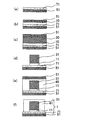
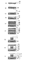
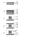
本発明により製造される光導波路1は、例えば、図1(d)や図3(d)に示すように、発色性を持たせるために発色剤を含有させたクラッド11がコアパタン31と同一パタンに形成されたものであり、図1(f)や図3(e)のようにパタン化された上部クラッド層41を有したものや接着層70を有したものであっても良い。また、本発明により製造される光電気複合基板2は、電気配線板60と光導波路を複合化されたもので電気配線板60上に光導波路1をビルドアップ形成したものである。更には図2(i)に示すように電気配線板60上に接着層70を形成し、その上に、光導波路を形成したものであっても良く、接着層70はクラッド層形成用材料を用いても良い。
(Optical waveguide and photoelectric composite substrate)
An optical waveguide and an optoelectric composite substrate obtained by the method for manufacturing an optical waveguide and an optoelectric composite substrate of the present invention will be described.
In the
光導波路の製造方法の第1工程
本発明の光導波路1の製造方法に係る第1工程は、基材50上に感光性の前記発色性のクラッド層10と感光性の前記コア層30とを積層する工程(A)と、工程(A)の後、該発色性のクラッド層10及び該コア層30を同時にパタン露光し、次いで、該発色性の下部クラッド層10の硬化していない部分及び該コア層30の硬化していない部分を現像除去することによって、パタン化された該発色性のクラッド層11及びパタン化された該コア層31からなる前記略直方体形状部材を形成する工程(B)とを含むこと、又は基材50上に下部クラッド層を形成し、該下部クラッド層上に、感光性の前記コア層30と感光性の前記発色性のクラッド層10とを積層する工程(C)と、工程(C)の後、該発色性のクラッド層10及び該コア層30を同時にパタン露光し、次いで、該発色性のクラッド層10の硬化していない部分及び該コア層30の硬化していない部分を現像除去することによって、パタン化された該発色性のクラッド層11及びパタン化された該コア層31からなる前記略直方体形状部材を形成する工程(D)とを含むことが好ましい。
また、必要に応じ、工程(A)において、前記基材50上に前記発色性のクラッド層10を、接着層70を介して積層しても良い。
以下、パタン化された発色性のクラッド層を「発色性のクラッドパタン」といい、パタン化されたコア層を「コアパタン」という。
First Step of Manufacturing Method of Optical Waveguide The first step of the manufacturing method of the
In addition, in the step (A), the color-forming
Hereinafter, the patterned color-forming clad layer is referred to as “color-forming clad pattern”, and the patterned core layer is referred to as “core pattern”.
光導波路の製造方法の第2工程
本発明に係る第1工程に続く第2工程は、前記第1工程中の工程(B)又は工程(D)の後に、前記コアパタン31及び発色性のクラッドパタン11からなる略直方体形状部材側から前記上部クラッド層40を積層する工程(E)を含むことが好ましく、この工程(E)後に、前記上部クラッド層を全面露光して露光後の上部クラッド層を形成する工程(F1)及び前記上部クラッド層をパタン露光してパタン化された該上部クラッド層を形成する工程(F2)のいずれかの工程(F)を含むことがさらに好ましい。
以下、パタン化された上部クラッド層を「上部クラッドパタン」という。
Second Step of Manufacturing Method of Optical Waveguide The second step following the first step according to the present invention is the step of (B) or (D) in the first step, followed by the
Hereinafter, the patterned upper clad layer is referred to as an “upper clad pattern”.
本発明の光導波路の製造方法の各工程を、以下、図面に基づいて説明する。図1は、本発明の光導波路1の製造方法の一例を説明する図である。
工程(A)
まず、図1(a)に示すように、基材50となるキャリアフィルム51の上面に所望により接着層70となる接着補助クラッド71を積層する。このとき接着層70付きの基材50を用いても良い。次に、接着補助クラッド71の上面に発色性のクラッド層10を積層する(図1(b))。但し、キャリアフィルム51と発色性のクラッド層10に十分な接着性がある場合には、キャリアフィルム51の上面に発色性のクラッド層10を直接積層しても良い。発色性のクラッド層10の積層方法は、特に限定されず公知の方法によれば良く、例えば、発色性のクラッド層10形成用樹脂組成物の塗布又は発色性のクラッド層10形成用樹脂フィルムのラミネートにより形成すれば良い。
次いで、図1(c)に示すように、発色性のクラッド層10の上面にコア層30を積層する。コア層30の積層方法は、特に限定されず公知の方法によれば良い。
工程(A)の好ましい方法としては、例えば、発色性のクラッド層10の形成材料をスピンコート等により基材50又は接着層70上に塗布し、プリベイクを行った後、発色性のクラッド層10の上面にコア層30の形成材料をスピンコート等によって塗布することにより形成できる。
また、発色性のクラッド層10形成用樹脂フィルムとコア層30形成用樹脂フィルム同士をラミネート等により貼り合わせて形成後、基材50又は接着層70の上面に貼り合わせたり、基材50又は接着層70の上面に発色性のクラッド層10形成用樹脂フィルムとコア層30形成用樹脂フィルムを順次貼り合わせたりしても良い。ここで、ラミネートに用いる発色性のクラッド層10形成用樹脂フィルムの形成方法としては、例えば、発色性のクラッド層形成用樹脂組成物を溶媒に溶解して、キャリアフィルム51に塗布し、溶媒を除去することにより容易に製造することができる。ラミネートに用いるコア層30形成用樹脂フィルムも同様にコア層30形成用樹脂組成物を溶媒に溶解して、キャリアフィルム51に塗布し、溶媒を除去することにより容易に製造することができる。
Each process of the manufacturing method of the optical waveguide of this invention is demonstrated based on drawing below. FIG. 1 is a diagram illustrating an example of a method for manufacturing an
Process (A)
First, as shown in FIG. 1A, an auxiliary bonding clad 71 to be an
Next, as shown in FIG. 1C, a
As a preferred method of the step (A), for example, a material for forming the color-forming
Further, after forming the color-forming
工程(B)
次に、得られた発色性のクラッド層10とコア層30との積層体を同時にパタン露光し、次いで、発色性のクラッド層10の硬化していない部分及びコア層30の硬化していない部分を現像除去して、図1(d)に示す、発色性のクラッドパタン11付のパタン化されたコア層(コアパタン)31からなる略直方体形状部材を形成する。
基材50上に接着層70として接着補助クラッド層71を用いる場合は、通常、接着補助クラッド層71はパタン露光されることなく基材50上に残されるが、必要に応じてパタン露光しても良い。
Process (B)
Next, the laminate of the resulting color-forming
When the auxiliary
工程(C)
まず、基材50となるキャリアフィルム51の上面に下部クラッド層20を積層し、硬化する。このときの下部クラッド層20は接着補助クラッド層71を用いても良い。通常、この下部クラッド層20はパタン露光されることなく基材50上に残されるが、必要に応じてパタン露光し、下部クラッドパタンとしても良い。
次に、下部クラッド層20の上面にコア層30を積層する。コア層の積層方法は、特に限定されず公知の方法によれば良く、例えば、コア層30形成用樹脂組成物の塗布又はコア層30形成用樹脂フィルムのラミネートにより形成すれば良い。
次いで、コア層30の上面に発色性のクラッド層10を積層する。発色性のクラッド層10の積層方法は、特に限定されず公知の方法によれば良い。
工程(C)の好ましい方法としては、例えば、コア層30の形成材料をスピンコート等により下部クラッド層20上に塗布し、プリベイクを行った後、コア層30の上面に発色性のクラッド層10の形成材料をスピンコート等によって塗布することにより形成できる。
また、発色性のクラッド層10形成用樹脂フィルムとコア層30形成用樹脂フィルム同士をラミネート等により貼り合わせて形成後、コア層30側から下部クラッド層20の上面に貼り合わせたり、下部クラッド層20の上面にコア層30形成用樹脂フィルムと発色性のクラッド層10形成用樹脂フィルムを順次貼り合わせたりしても良い。ここで、ラミネートに用いる発色性のクラッド層10形成用樹脂フィルム例えば、発色性のクラッド層10形成用樹脂組成物を溶媒に溶解して、キャリアフィルム51に塗布し、溶媒を除去することにより容易に製造することができる。ラミネートに用いるコア層30形成用樹脂フィルムも同様にコア層30形成用樹脂組成物を溶媒に溶解して、キャリアフィルム51に塗布し、溶媒を除去することにより容易に製造することができる。
Process (C)
First, the lower
Next, the
Next, the color-forming
As a preferred method of the step (C), for example, a material for forming the
Further, after forming the color-developing
工程(D)
次に、得られたコア層30と発色性のクラッド層10との積層体を同時にパタン露光し、次いで、コア層30の硬化していない部分及び発色性のクラッド層10の硬化していない部分を現像除去して、発色性のクラッドパタン11付きのコアパタン31からなる略直方体形状部材を形成する。このときの現像除去方法としてはコア層30と発色性のクラッド層10を同一の現像液にてパタン化しても良く、コア層30と発色性のクラッド層10を異なる現像液を用いて段階的にパタン化しても良い。
Process (D)
Next, the laminated body of the obtained
工程(E)
次いで、図1(e)に示すように、略直方体形状部材である発色性のクラッドパタン11及びコアパタン31を、工程(A)の場合は、コアパタン側から、コアパタン31の上面と側面、及び発色性のクラッドパタン11の側面を覆って上部クラッド層40を積層する。工程(C)の場合は発色性のクラッドパタン11側から、発色性のクラッドパタン11の上面と側面、及びコアパタン31の側面を覆って上部クラッド層40を積層する。本発明においては、上部クラッド層40の形成方法は特に限定されず、例えば、上部クラッド層40形成用樹脂組成物の塗布又は上部クラッド層形成用樹脂フィルムのラミネートにより形成すれば良い。
塗布による場合には、その方法は限定されず、例えば、後述する成分を含有する樹脂組成物を常法により塗布すれば良い。また、ラミネートに用いる上部クラッド層40形成用樹脂フィルムは、例えば、上述のクラッド層形成用樹脂フィルムと同様に上部クラッド層40形成用樹脂組成物を溶媒に溶解して、キャリアフィルム51に塗布し、溶媒を除去することにより容易に製造することができる。図1(e)は、このキャリアフィルム51付きの上部クラッド層40形成用樹脂フィルムを用いた場合を示す。また、所望により、上部クラッド層40の表面保護等の目的で、上部クラッド層40の上面にキャリアフィルム51を貼着したままにしておいても良く、最終的に、基材50、キャリアフィルム51は除去しても良い。これらにより光導波路1が得られる。
Process (E)
Next, as shown in FIG. 1 (e), the color-forming
In the case of coating, the method is not limited. For example, a resin composition containing the components described later may be coated by a conventional method. The resin film for forming the upper clad
工程(F)
前記工程(E)後に、前記上部クラッド層を全面露光して露光後の上部クラッド層40を形成する工程(F1)及び前記上部クラッド層40をパタン露光してパタン化された該上部クラッド層40を形成する工程(F2)のいずれかの工程(F)を含むことがさらに好ましい。
本発明方法により得られた光導波路1は、図1(d)に示すように、コアパタン31と同一パタンで発色性のクラッドパタン11が形成されるため、発色性のクラッドパタン11の発色を検出することにより、コアパタン31を視認することが可能となる。
Process (F)
After the step (E), the entire surface of the upper cladding layer is exposed to form an exposed upper cladding layer 40 (F 1 ), and the
In the
本発明の光電気複合基板2は、上述の本発明方法により得られた光導波路1と電気配線板60とを複合化することにより得られるが、電気配線板60上に直接光導波路1を形成する方法が好ましい。
すなわち、本発明の好ましい光電気複合基板2の製造方法は、電気配線板60上に略直方体形状の発色性のクラッド層10、及び該発色性のクラッド層10の上面又は下面に搭載された略直方体形状のコア層30からなる略直方体形状部材を形成する第1の工程と、該略直方体形状部材の上面と側面を覆う上部クラッド層40を形成する第2の工程とを含むことを特徴とする。
The optoelectric
That is, the preferable method for manufacturing the optoelectric
光電気複合基板の製造方法の第1工程
本発明の光電気複合基板2の製造方法に係る第1工程は、前記電気配線板60上に感光性の前記発色性のクラッド層10と感光性の前記コア層30とを積層する工程(A*)と、工程(A*)の後、該発色性のクラッド層10及び該コア層30を同時にパタン露光し、次いで、該発色性のクラッド層10の硬化していない部分及び該コア層30の硬化していない部分を現像除去することによって、発色性のクラッドパタン11及びコアパタン31からなる前記略直方体形状部材を形成する工程(B*)とを含むことが好ましく、又は電気配線板60上に下部クラッド層20を形成し、該下部クラッド層20上に、感光性の前記コア層30と感光性の前記発色性のクラッド層10とを積層する工程(C*)と、工程(C*)の後、該発色性のクラッド層10及び該コア層30を同時にパタン露光し、次いで、該発色性のクラッド層10の硬化していない部分及び該コア層30の硬化していない部分を現像除去することによって、パタン化された該発色性のクラッド層10及びパタン化された該コア層30からなる前記略直方体形状部材を形成する工程(D*)とを含むことが好ましい。
このときの現像除去方法としてはコア層30と発色性のクラッド層10を同一の現像液にてパタン化しても良く、コア層30と発色性のクラッド層10を異なる現像液を用いて段階的にパタン化しても良い。
また、必要に応じ、工程(A*)において、前記基材50上に前記発色性のクラッド層10を、接着層70を介して積層しても良い。
First Step of Manufacturing Method of Photoelectric Composite Substrate The first step according to the method of manufacturing the photoelectric
As a method for developing and removing at this time, the
In addition, in the step (A * ), the color-forming
光電気複合基板の製造方法の第2工程
本発明に係る第1工程に続く第2工程は、前記第1工程中の工程(B*)又は工程(D*)の後に、前記コアパタン31側、又は前記コアパタン31及び発色性のクラッドパタン11からなる略直方体形状部材側から前記上部クラッド層40を積層する工程(E*)を含むことが好ましく、この工程(E*)後に、前記上部クラッド層を全面露光して露光後の上部クラッド層を形成する工程(F1 *)及び前記上部クラッド層をパタン露光してパタン化された該上部クラッド層を形成する工程(F2 *)のいずれかの工程(F*)を含むことがさらに好ましい。
Second step of manufacturing method of optoelectric composite substrate The second step following the first step according to the present invention is the step (B * ) or the step (D * ) in the first step, the
本発明の光電気複合基板の製造方法の各工程を、以下、図面に基づいて説明する。図2は、本発明の光電気複合基板2の製造方法の一例を説明する図である。
工程(A * )〜(D * )
図2に示す方法は、図1(a)に示すキャリアフィルム51を電気配線板60に変更したものであり、図1と同様に、電気配線板60の上面に下部クラッド層20を積層する。次に、下部クラッド層20の上面にコアパタン31と発色性のクラッドパタン11からなる略直方体形状部材を形成し、図1と同様に、略直方体形状部材の上面と側面を上部クラッド層40で覆い、さらに上部クラッドパタン41を形成して光電気複合基板2が得られる。さらには図1(a)のキャリアフィルム51を電気配線板60として図1と同様に光導波路1を形成すれば図2(g)の発色性のクラッドパタン11とコアパタン31の位置が入れ替わった光電気複合基板を得ることができる。本発明方法により得られた光電気複合基板2は、図2(g)に示すように、コアパタン31と同一パタンで発色性のクラッドパタン11が形成されるため、発色性のクラッドパタン11からの発色を検出することにより、コアパタン31を視認することが可能となる。
Each step of the method for manufacturing an optoelectric composite substrate of the present invention will be described below with reference to the drawings. FIG. 2 is a diagram for explaining an example of a method for producing the photoelectric
Process (A * ) to (D * )
In the method shown in FIG. 2, the
以下、光導波路及び光電気複合基板の各構成部分について説明する。
(クラッド層)
以下、本発明で使用される発色性のクラッド層10、下部クラッド層20、上部クラッド層40について説明する。下部クラッド層10、上部クラッド層40としては、クラッド層形成用樹脂組成物又はクラッド層形成用樹脂フィルムを用いることができる。発色性のクラッド層10における発色性に関しては下部クラッド層10及び上部クラッド層40の組成に発色剤を付与することによって得られる。発色剤については(発色性のクラッド層の発色剤)の欄で後述する。
本発明で用いられるクラッド層形成用樹脂組成物としては、使用されるコア層30より低屈折率で、光により硬化する樹脂組成物であれば特に限定されず、感光性樹脂組成物を好適に使用することができる。より好適にはクラッド層形成用樹脂組成物が、(a)キャリアポリマー、(b)光重合性化合物及び(c)光重合開始剤を含有する樹脂組成物により構成されることが好ましい。
Hereinafter, each component of the optical waveguide and the photoelectric composite substrate will be described.
(Clad layer)
Hereinafter, the color-forming
The resin composition for forming a cladding layer used in the present invention is not particularly limited as long as it is a resin composition having a lower refractive index than that of the
ここで用いる(a)キャリアポリマーはクラッド層を形成し、該クラッド層の強度を確保するためのものであり、該目的を達成し得るものであれば特に限定されず、フェノキシ樹脂、エポキシ樹脂、(メタ)アクリル樹脂、ポリカーボネート樹脂、ポリアリレート樹脂、ポリエーテルアミド、ポリエーテルイミド、ポリエーテルスルホン等、あるいはこれらの誘導体などが挙げられる。これらのキャリアポリマーは1種単独でも、また2種以上を混合して用いても良い。上記で例示したキャリアポリマーのうち、耐熱性が高いとの観点から、主鎖に芳香族骨格を有することが好ましく、特にフェノキシ樹脂が好ましい。また、3次元架橋し、耐熱性を向上できるとの観点からは、エポキシ樹脂、特に室温(25℃)で固形のエポキシ樹脂が好ましい。さらに、後に詳述する(b)光重合性化合物との相溶性が、クラッド層形成用樹脂組成物の透明性を確保するために重要であるが、この点からは上記フェノキシ樹脂及び(メタ)アクリル樹脂が好ましい。なお、ここで(メタ)アクリル樹脂とは、アクリル樹脂及びメタクリル樹脂を意味するものである。 The carrier polymer (a) used here is for forming a clad layer and ensuring the strength of the clad layer, and is not particularly limited as long as the object can be achieved, phenoxy resin, epoxy resin, (Meth) acrylic resin, polycarbonate resin, polyarylate resin, polyether amide, polyether imide, polyether sulfone, etc., or derivatives thereof. These carrier polymers may be used alone or in combination of two or more. Of the carrier polymers exemplified above, the main chain preferably has an aromatic skeleton, and particularly preferably a phenoxy resin, from the viewpoint of high heat resistance. From the viewpoint of three-dimensional crosslinking and improving heat resistance, an epoxy resin, particularly a solid epoxy resin at room temperature (25 ° C.) is preferable. Furthermore, the compatibility with the photopolymerizable compound (b) described in detail later is important for ensuring the transparency of the resin composition for forming a cladding layer. From this point, the phenoxy resin and (meth) Acrylic resin is preferred. Here, (meth) acrylic resin means acrylic resin and methacrylic resin.
フェノキシ樹脂の中でも、ビスフェノールA、ビスフェノールA型エポキシ化合物又はそれらの誘導体、及びビスフェノールF、ビスフェノールF型エポキシ化合物又はそれらの誘導体を共重合成分の構成単位として含むものは、耐熱性、密着性及び溶解性に優れるため好ましい。ビスフェノールA又はビスフェノールA型エポキシ化合物の誘導体としては、テトラブロモビスフェノールA、テトラブロモビスフェノールA型エポキシ化合物等が好適に挙げられる。また、ビスフェノールF又はビスフェノールF型エポキシ化合物の誘導体としては、テトラブロモビスフェノールF、テトラブロモビスフェノールF型エポキシ化合物等が好適に挙げられる。ビスフェノールA/ビスフェノールF共重合型フェノキシ樹脂の具体例としては、東都化成(株)製「フェノトートYP−70」(商品名)が挙げられる。 Among phenoxy resins, those containing bisphenol A, bisphenol A type epoxy compounds or derivatives thereof, and bisphenol F, bisphenol F type epoxy compounds or derivatives thereof as a constituent unit of the copolymer component are heat resistant, adhesive and soluble. It is preferable because of its excellent properties. Preferred examples of the bisphenol A or bisphenol A type epoxy compound include tetrabromobisphenol A and tetrabromobisphenol A type epoxy compounds. Moreover, as a derivative of bisphenol F or a bisphenol F-type epoxy compound, tetrabromobisphenol F, a tetrabromobisphenol F-type epoxy compound, etc. are mentioned suitably. Specific examples of the bisphenol A / bisphenol F copolymer type phenoxy resin include “Phenotote YP-70” (trade name) manufactured by Toto Kasei Co., Ltd.
室温(25℃)で固形のエポキシ樹脂としては、例えば、東都化学(株)製「エポトートYD−7020、エポトートYD−7019、エポトートYD−7017」(いずれも商品名)、ジャパンエポキシレジン(株)製「エピコート1010、エピコート1009、エピコート1008」(いずれも商品名)などのビスフェノールA型エポキシ樹脂が挙げられる。 As an epoxy resin solid at room temperature (25 ° C.), for example, “Epototo YD-7020, Epototo YD-7019, Epototo YD-7007” (all trade names) manufactured by Toto Chemical Co., Ltd., Japan Epoxy Resins Co., Ltd. Examples thereof include bisphenol A type epoxy resins such as “Epicoat 1010, Epicoat 1009, Epicoat 1008” (all trade names).
次に、(b)光重合性化合物としては、光の照射によって重合するものであれば特に限定されず、分子内にエチレン性不飽和基を有する化合物や分子内に2つ以上のエポキシ基を有する化合物などが挙げられる。
分子内にエチレン性不飽和基を有する化合物としては、(メタ)アクリレート、ハロゲン化ビニリデン、ビニルエーテル、ビニルピリジン、ビニルフェノール等が挙げられるが、これらの中で、透明性と耐熱性の観点から、(メタ)アクリレートが好ましい。
(メタ)アクリレートとしては、1官能性のもの、2官能性のもの、3官能性以上の多官能性のもののいずれをも用いることができる。なお、ここで(メタ)アクリレートとは、アクリレート及びメタクリレートを意味するものである。
Next, (b) the photopolymerizable compound is not particularly limited as long as it is polymerized by light irradiation, and a compound having an ethylenically unsaturated group in the molecule or two or more epoxy groups in the molecule. And the like.
Examples of the compound having an ethylenically unsaturated group in the molecule include (meth) acrylate, vinylidene halide, vinyl ether, vinyl pyridine, vinyl phenol, etc., among these, from the viewpoint of transparency and heat resistance, (Meth) acrylate is preferred.
As the (meth) acrylate, any of monofunctional, bifunctional, trifunctional or higher polyfunctional ones can be used. Here, (meth) acrylate means acrylate and methacrylate.
分子内に2つ以上のエポキシ基を有する化合物としては、ビスフェノールA型エポキシ樹脂等の2官能又は多官能芳香族グリシジルエーテル、ポリエチレングリコール型エポキシ樹脂等の2官能又は多官能脂肪族グリシジルエーテル、水添ビスフェノールA型エポキシ樹脂等の2官能脂環式グリシジルエーテル、フタル酸ジグリシジルエステル等の2官能芳香族グリシジルエステル、テトラヒドロフタル酸ジグリシジルエステル等の2官能脂環式グリシジルエステル、N,N−ジグリシジルアニリン等の2官能又は多官能芳香族グリシジルアミン、アリサイクリックジエポキシカルボキシレート等の2官能脂環式エポキシ樹脂、2官能複素環式エポキシ樹脂、多官能複素環式エポキシ樹脂、2官能又は多官能ケイ素含有エポキシ樹脂などが挙げられる。これらの(b)光重合性化合物は、単独で又は2種類以上組み合わせて用いることができる。 Examples of the compound having two or more epoxy groups in the molecule include bifunctional or polyfunctional aromatic glycidyl ethers such as bisphenol A type epoxy resins, bifunctional or polyfunctional aliphatic glycidyl ethers such as polyethylene glycol type epoxy resins, and water. Bifunctional alicyclic glycidyl ether such as bisphenol A type epoxy resin, bifunctional aromatic glycidyl ester such as diglycidyl phthalate, bifunctional alicyclic glycidyl ester such as tetrahydrophthalic acid diglycidyl ester, N, N- Bifunctional or polyfunctional aromatic glycidylamine such as diglycidylaniline, bifunctional alicyclic epoxy resin such as alicyclic diepoxycarboxylate, bifunctional heterocyclic epoxy resin, polyfunctional heterocyclic epoxy resin, bifunctional Or polyfunctional silicon-containing epoxy resin It is. These (b) photopolymerizable compounds can be used alone or in combination of two or more.
次に(c)成分の光重合開始剤としては、特に制限はなく、例えば(b)成分にエポキシ化合物を用いる場合の開始剤として、アリールジアゾニウム塩、ジアリールヨードニウム塩、トリアリールスルホニウム塩、トリアリルセレノニウム塩、ジアルキルフェナジルスルホニウム塩、ジアルキル−4−ヒドロキシフェニルスルホニウム塩、スルホン酸エステルなどが挙げられる。 Next, the photopolymerization initiator of component (c) is not particularly limited. For example, as an initiator when an epoxy compound is used as component (b), aryldiazonium salt, diaryliodonium salt, triarylsulfonium salt, triallyl Examples include selenonium salts, dialkylphenazylsulfonium salts, dialkyl-4-hydroxyphenylsulfonium salts, and sulfonate esters.
また、(b)成分に分子内にエチレン性不飽和基を有する化合物を用いる場合の開始剤としては、ベンゾフェノン等の芳香族ケトン、2−エチルアントラキノン等のキノン類、ベンゾインメチルエーテル等のベンゾインエーテル化合物、ベンゾイン等のベンゾイン化合物、ベンジルジメチルケタール等のベンジル誘導体、2−(o−クロロフェニル)−4,5−ジフェニルイミダゾール二量体等の2,4,5−トリアリールイミダゾール二量体、2−メルカプトベンゾイミダゾール等のベンゾイミダゾール類、ビス(2,4,6−トリメチルベンゾイル)フェニルフォスフィンオキサイド等のフォスフィンオキサイド類、9−フェニルアクリジン等のアクリジン誘導体、N−フェニルグリシン、N−フェニルグリシン誘導体、クマリン系化合物などが挙げられる。また、ジエチルチオキサントンとジメチルアミノ安息香酸の組み合わせのように、チオキサントン系化合物と3級アミン化合物とを組み合わせても良い。なお、クラッド層の透明性を向上させる観点からは、上記化合物のうち、芳香族ケトン及びフォスフィンオキサイド類が好ましい。
これらの(c)光重合開始剤は、単独で又は2種類以上組み合わせて用いることができる。
In addition, as an initiator when a compound having an ethylenically unsaturated group in the molecule is used as the component (b), aromatic ketones such as benzophenone, quinones such as 2-ethylanthraquinone, benzoin ethers such as benzoin methyl ether Compounds, benzoin compounds such as benzoin, benzyl derivatives such as benzyldimethyl ketal, 2,4,5-triarylimidazole dimers such as 2- (o-chlorophenyl) -4,5-diphenylimidazole dimer, 2- Benzimidazoles such as mercaptobenzimidazole, phosphine oxides such as bis (2,4,6-trimethylbenzoyl) phenylphosphine oxide, acridine derivatives such as 9-phenylacridine, N-phenylglycine, N-phenylglycine derivatives , Coumarin compound And the like. Moreover, you may combine a thioxanthone type compound and a tertiary amine compound like the combination of diethyl thioxanthone and dimethylaminobenzoic acid. Of the above compounds, aromatic ketones and phosphine oxides are preferable from the viewpoint of improving the transparency of the cladding layer.
These (c) photopolymerization initiators can be used alone or in combination of two or more.
(a)キャリアポリマーの配合量は、(a)成分及び(b)成分の総量中、5〜80質量%とすることが好ましい。また、(b)光重合性化合物の配合量は、(a)及び(b)成分の総量中、95〜20質量%とすることが好ましい。
この(a)成分及び(b)成分の配合量として、(a)成分が5質量%以上であり、(b)成分が95質量%以下であると、樹脂組成物を容易にフィルム化することができる。一方、(a)成分が80質量%以下あり、(b)成分が20質量%以上であると、(a)キャリアポリマーを絡み込んで硬化させることが容易にでき、光導波路1を形成する際に、パタン形成性が向上し、かつ光硬化反応が十分に進行する。以上の観点から、この(a)成分及び(b)成分の配合量として、(a)及び(b)成分の総量中、(a)成分10〜85質量%、(b)成分90〜15質量%がより好ましく、(a)成分20〜70質量%、(b)成分80〜30質量%がさらに好ましい。
(c)光重合開始剤の配合量は、(a)成分及び(b)成分の総量100質量部に対して、0.1〜10質量部とすることが好ましい。この配合量が0.1質量部以上であると、光感度が十分であり、一方10質量部以下であると、露光時に感光性樹脂組成物の表層での吸収が増大することがなく、内部の光硬化が十分となる。さらに、光導波路1として使用する際には、重合開始剤自身の光吸収の影響により伝搬損失が増大することもなく好適である。以上の観点から、(c)光重合開始剤の配合量は、0.2〜5質量部とすることがより好ましい。
(A) It is preferable that the compounding quantity of a carrier polymer shall be 5-80 mass% in the total amount of (a) component and (b) component. Moreover, it is preferable that the compounding quantity of (b) photopolymerizable compound shall be 95-20 mass% in the total amount of (a) and (b) component.
As a blending amount of the component (a) and the component (b), when the component (a) is 5% by mass or more and the component (b) is 95% by mass or less, the resin composition is easily formed into a film. Can do. On the other hand, when the (a) component is 80% by mass or less and the (b) component is 20% by mass or more, (a) the carrier polymer can be easily entangled and cured, and the
(C) It is preferable that the compounding quantity of a photoinitiator shall be 0.1-10 mass parts with respect to 100 mass parts of total amounts of (a) component and (b) component. When the blending amount is 0.1 parts by mass or more, the photosensitivity is sufficient, while when it is 10 parts by mass or less, the absorption in the surface layer of the photosensitive resin composition does not increase during exposure, and the internal Is sufficiently cured. Further, when used as the
下部クラッド層20の厚さに関しては、乾燥後の厚さで、5〜500μmの範囲が好ましい。5μm以上であると、光の閉じ込めに必要なクラッド厚さが確保でき、500μm以下であると、膜厚を均一に制御することが容易である。
上部クラッド層40の厚さに関しては、下部クラッド層20の厚さと同一であっても異なっても良いが、略直方体形状部材を埋め込むために、上部クラッド層40の厚さは、発色性のクラッド層10の厚さ及びコア層30の厚さを合計した厚さよりも厚くすることが好ましい。
発色性のクラッド層10の厚さに関しては、接着層70に下部クラッド層10や接着補助用のクラッド層71を用いる場合やコア層30上に発色性のクラッド層10を形成する場合には、厚みの制限はないが、乾燥後の厚さで、1〜500μmの範囲が好ましい。500μm以下であると、膜厚を均一に制御することが容易である。また、基材50や電気配線板60上に直接発色性のクラッド層10を形成する場合には、5μm以上であると、光の閉じ込めに必要なクラッド厚さが確保できる。また、コア層30を露光する時の露光量において、発色性のクラッド層10を硬化が可能な膜厚であれば良く、この観点から、発色性のクラッド層10の厚さは、5〜50μmの範囲であることがより好ましい。
Regarding the thickness of the
The thickness of the upper clad
Regarding the thickness of the color-forming
(発色性のクラッド層の発色剤)
発色性のクラッド層10は、下部クラッド層20及び上部クラッド層40及び接着補助クラッド層71の組成に発色剤を付与することによって得られる。発色剤には大きく分けて、光放出型、光吸収型、併用型がある。以下に発色性のクラッド層10に発色性を付与させるための発色剤について説明する。
(光放出型の発色剤)
発色性のクラッドに導入する光放出型の発色剤の種類としては、特に制限されるものではないが、例えば、蛍光剤、りん光剤、蓄光剤、蛍光性又はりん光性の光重合開始剤、蛍光性又はりん光性の光増感剤、それらを2種類以上組み合わせたものなどが挙げられる。特に露光光源及びクラッドを発色させるために紫外線ランプを用いる場合には、蛍光剤、りん光剤、蓄光剤、蛍光性又はりん光性の光増感剤を用いることが好ましく、導入する光変換型の紫外線吸収剤量は、光伝搬損失に影響のない範囲であればよい。
(Coloring agent for coloring layer)
The color-forming
(Light-emitting color former)
The type of light-emitting color former introduced into the color-forming clad is not particularly limited, and examples thereof include fluorescent agents, phosphorescent agents, phosphorescent agents, fluorescent or phosphorescent photopolymerization initiators. , Fluorescent or phosphorescent photosensitizers, and combinations of two or more thereof. In particular, when an ultraviolet lamp is used to color the exposure light source and the cladding, it is preferable to use a fluorescent agent, a phosphorescent agent, a phosphorescent agent, a fluorescent or phosphorescent photosensitizer, and a light conversion type to be introduced. The amount of the ultraviolet absorber may be in a range that does not affect the light propagation loss.
(光吸収型の発色剤)
発色性のクラッドに導入する光吸収型の発色剤の種類としては、特に制限されるものではないが、熱エネルギー変換型の紫外線吸収剤、着色剤、それらを2種類以上組み合わせたものなどが挙げられる。熱エネルギー変換型の紫外線吸収剤の場合は、接着層、下部クラッド層、基材、電気配線板に、紫外線による発光性があれば、黒色に発色させることが可能となる。着色剤であれば、可視光領域のクラッドの発光や呈色によって位置を視認することができる。導入する光吸収型の発色剤の量は、光伝搬損失に影響のない範囲であればよい。
(併用型の発色剤)
前述した光放出型の発色剤と、光吸収型の発色剤を視認性の調整のために適宜組み合わせてもよく、導入する光放出型及び光吸収型の発色剤の量は、光伝搬損失に影響のない範囲であればよい。
(Light absorbing color former)
The type of light-absorbing color former to be introduced into the color-forming clad is not particularly limited, but examples include thermal energy conversion type ultraviolet absorbers, colorants, and combinations of two or more of them. It is done. In the case of a heat energy conversion type ultraviolet absorber, if the adhesive layer, the lower cladding layer, the base material, and the electric wiring board have a light emitting property due to ultraviolet rays, it is possible to develop a black color. If it is a coloring agent, a position can be visually recognized by light emission and coloration of the clad in a visible light region. The amount of the light absorbing color former to be introduced may be in a range that does not affect the light propagation loss.
(Combined color former)
The light-emitting color former and the light-absorbing color former may be appropriately combined for the purpose of adjusting the visibility. The amount of the light-emitting and light-absorbing colorants to be introduced depends on the light propagation loss. It may be in a range without influence.
(コア層形成用樹脂組成物及びコア層形成用樹脂フィルム)
コア層30形成用樹脂組成物としては、コアパタン31が下部クラッド層20、接着補助用クラッド層71、発色性のクラッド層10、上部クラッド層40より高屈折率であるように設計され、活性光線によりコアパタン31を形成し得る樹脂組成物を用いることができ、感光性樹脂組成物が好適である。具体的には、前記クラッド層形成用樹脂組成物で用いたのと同様の樹脂組成物を用いることが好ましい。
塗布による場合には、方法は限定されず、前記樹脂組成物を常法により塗布すれば良い。
(Core layer forming resin composition and core layer forming resin film)
As the resin composition for forming the
In the case of application, the method is not limited, and the resin composition may be applied by a conventional method.
以下、ラミネートに用いるコア層30形成用樹脂フィルムについて詳述する。
コア層30形成用樹脂フィルムは、前記樹脂組成物を溶媒に溶解して下部クラッド層20や発色性のクラッド層10に塗布し、溶媒を除去することにより容易に製造することができる。ここで用いる溶媒としては、該樹脂組成物を溶解し得るものであれば特に限定されず、例えば、アセトン、メチルエチルケトン、メチルセロソルブ、エチルセロソルブ、トルエン、N,N−ジメチルホルムアミド、N,N−ジメチルアセトアミド、プロピレングリコールモノメチルエーテル、プロピレングリコールモノメチルエーテルアセテート、シクロヘキサノン、N−メチル−2−ピロリドン等の溶媒又はこれらの混合溶媒を用いることができる。樹脂組成物溶液中の固形分濃度は、通常30〜80質量%であることが好ましい。
Hereinafter, the resin film for forming the
The resin film for forming the
コア層30形成用樹脂フィルムの厚さについては特に限定されず、乾燥後のコア層30の厚さが、通常は10〜100μmとなるように調整される。該フィルムの厚さが10μm以上であると、光導波路形成後の受発光素子又は光ファイバーとの結合において位置合わせトレランスが拡大できるという利点があり、100μm以下であると、光導波路形成後の受発光素子又は光ファイバーとの結合において、結合効率が向上するという利点がある。以上の観点から、該フィルムの厚さは、さらに30〜70μmの範囲であることが好ましい。
The thickness of the resin film for forming the
(キャリアフィルム)
クラッド層形成用樹脂フィルムの製造過程で用いられるキャリアフィルム51は、その材料については特に限定されず、種々のものを用いることができる。例えば、FR−4基板、ポリイミド基板、半導体基板、シリコン基板やガラス基板等を用いることができ、可撓性があるフレキシブルな材質でも、非可撓性の固い材質のものであっても良い。
また、キャリアフィルム51に可撓性を有する素材を用いることにより、フレキシブルな光電気複合部材を得ることができる。可撓性を有する素材の材料としては、特に限定されないが、柔軟性、強靭性を有するとの観点から、ポリエチレンテレフタレート、ポリブチレンテレフタレート、ポリエチレンナフタレート等のポリエステル、ポリエチレン、ポリプロピレン、ポリアミド、ポリカーボネート、ポリフェニレンエーテル、ポリエーテルサルファイド、ポリアリレート、液晶ポリマー、ポリスルホン、ポリエーテルスルホン、ポリエーテルエーテルケトン、ポリエーテルイミド、ポリアミドイミド、ポリイミドなどが好適に挙げられる。
フィルムの厚さは、目的とする柔軟性により適宜変えて良いが、5μm〜10mmであることが好ましく、柔軟性を必要とする場合は、5〜250μmであることが好ましい。5μm以上であると強靭性が得易いという利点があり、250μm以下であると十分な柔軟性が得られる。
(Carrier film)
The material of the
Moreover, a flexible photoelectric composite member can be obtained by using a flexible material for the
The thickness of the film may be appropriately changed depending on the intended flexibility, but is preferably 5 μm to 10 mm, and preferably 5 to 250 μm when flexibility is required. If it is 5 μm or more, there is an advantage that toughness can be easily obtained, and if it is 250 μm or less, sufficient flexibility can be obtained.
前記キャリアフィルム51の内、コア層30又は各種クラッド層形成用樹脂組成物塗膜の製造過程で用いるキャリアフィルム51は、また、後にコア層30又は各種クラッド層形成用樹脂組成物塗膜を剥離することが容易であり、かつ、耐熱性及び耐溶剤性を有するとの観点から、ポリエチレンテレフタレート等のポリエステル、ポリプロピレン、ポリエチレンなどが好適に挙げられる。この場合のキャリアフィルム51の厚さは、5〜50μmであることが好ましい。5μm以上であると、キャリアフィルム51としての強度が得やすいという利点があり、50μm以下であると、パタン形成時のマスクとのギャップが小さくなり、より微細なパタンが形成できるという利点がある。以上の観点から、塗膜の製造過程で用いるキャリアフィルム51の厚さは10〜40μmの範囲であることがより好ましく、15〜30μmであることが特に好ましい。
Of the
(電気配線板)
本発明において用いられる電気配線板60としては、特に限定されるものではなく、光電気複合基板2に用いられる種々の電気配線板60を用いることができ、例えば、電気配線板用の絶縁基板や、絶縁基板に電気配線が形成されているものや、多層の配線板をであっても良い。また、電気配線板60と発色性のクラッド層10や下部クラッド層20や上部クラッド層40に接着力がない場合、電気配線板表面に物理的な粗化処理や化学的な接着用皮膜の形成を適宜行っても良い。また電気配線板60上に接着層70、例えば接着補助クラッド層71を設けても良い。
(Electric wiring board)
The
(接着層)
電気配線板2や基材50と、接着力の弱い発色性のクラッド層10との接着する方法には、特に限定されないが、接着層70を介して積層する場合には接着層として接着剤または接着フィルム材料を使用することができ、その材料としては、両面テープ、ホットメルト接着剤、UVまたは熱硬化性着剤などが好適に挙げられる。
接着剤の材料としては、プリプレグ、ビルドアップ材、熱硬化接着剤、光硬化接着剤、それらを2種類以上組み合わせて積層したものなどが好適に挙げられる。光信号が接着層70を透過する場合の接着には高い透過率の接着層70が必要であり、その場合、接着層70の材料としては、特に限定されないが、各種クラッド層又は30形成用樹脂組成物、コア層30形成用樹脂組成物又は後述する接着剤を使用することがより好ましい。
また、光信号が透過する部分の接着には高い透過率の接着剤または接着フィルムが必要であり、接着剤または接着フィルムの材料としては、特に限定されないが、(PCT/JP2008/05465)に記載の接着フィルムや、発色性のクラッドパタンと識別できる接着補助クラッド層71を使用することがより好ましい。
接着層70の厚みは特に限定はないが、0.1〜100μmであることが好ましく、0.1〜50μmであることがより好ましい。
(Adhesive layer)
The method for adhering the
Preferable examples of the adhesive material include prepregs, build-up materials, thermosetting adhesives, photo-curing adhesives, and laminates obtained by combining two or more thereof. Adhesion when an optical signal passes through the
Further, an adhesive or adhesive film having a high transmittance is required for adhesion of a portion through which an optical signal is transmitted, and the material of the adhesive or adhesive film is not particularly limited, but is described in (PCT / JP2008 / 05465). It is more preferable to use an adhesive auxiliary clad
Although the thickness of the
(接着層70用接着剤)
接着層70用接着剤としては、ビスフェノールA型エポキシ樹脂、ビスフェノールF型エポキシ樹脂、フェノールノボラック型エポキシ樹脂、クレゾールノボラック型エポキシ樹脂、多官能エポキシ樹脂、アミン型エポキシ樹脂、アミン型エポキシ樹脂等のエポキシ樹脂の1種又は2種以上(p)と、多官能フェノール類(特に、ノボラック型あるいはレゾール型のフェノール系樹脂)、アミン類、イミダゾール化合物、酸無水物、有機リン化合物及びこれらのハロゲン化物、ポリアミド、ポリスルフィド、三フッ化ホウ素等の硬化剤の1種又は2種以上(q)と、アクリル系共重合体、アクリルゴム、アクリロニトリルブタジエンゴム、シリコーンゴム等のゴム、シリコーン樹脂、シリコーン変性ポリアミドイミド等のシリコーン変性樹脂、ポリウレタン、ポリイミド、ポリイミドアミド等の高分子化合物の1種又は2種以上(r)と、水酸化アルミニウム、水酸化マグネシウム、炭酸カルシウム、炭酸マグネシウム、ケイ酸カルシウム、ケイ酸マグネシウム、酸化カルシウム、酸化マグネシウム、酸化アルミニウム、結晶質シリカ、非晶質シリカ、アクリロニトリルブタジエンゴムフィラー、シリコーンゴムフィラー等のフィラーの1種又は2種以上(s)と、第三級アミン、イミダゾール類、第四級アンモニウム塩等の硬化促進剤の1種又は2種以上(t)とを含む接着剤が好ましい。
(p)成分と(q)成分との配合量比はエポキシ当量と水酸基当量の当量比で0.70/0.30〜0.30/0.70となるのが好ましく、[{(p)成分+(q)成分}/(r)成分]配合量(質量部)比は0.24〜1.0であることが好ましく、{(p)成分+(q)成分}100質量部に対して、(s)成分1〜50質量部、(t)成分5.0質量部以下であることが好ましい。また、必要に応じ、シラン系、チタン系、アルミニウム系等のカップリング剤、イオン捕捉剤等を適宜配合しても良い。
(Adhesive for adhesive layer 70)
Examples of the adhesive for the
The blending ratio of the component (p) and the component (q) is preferably 0.70 / 0.30 to 0.30 / 0.70 in terms of the equivalent ratio of epoxy equivalent and hydroxyl equivalent, [{(p) Component + (q) component} / (r) component] ratio (parts by mass) is preferably 0.24 to 1.0, and {part (p) component + (q) component} is 100 parts by mass. The component (s) is preferably 1 to 50 parts by mass and the component (t) is 5.0 parts by mass or less. Moreover, you may mix | blend a coupling agent, ion trapping agents, etc., such as a silane type, a titanium type, and aluminum type, as needed.
(接着補助クラッド層)
接着層70として用いられる接着補助クラッド層71の材料は、特に限定されず、種々のものを用いることができるが、下部クラッド層20、上部クラッド層40、発色性の下部クラッド層10形成用樹脂組成物が好ましい。
接着補助クラッド71の厚みは特に限定されるものではないが、1〜50μmであると下部クラッド層10又は下部クラッドパタン11との十分な接着を確保することが出来る。
(Adhesive auxiliary cladding layer)
The material of the adhesion auxiliary clad
The thickness of the adhesion auxiliary clad 71 is not particularly limited, but if it is 1 to 50 μm, sufficient adhesion to the lower
(電気配線板と光導波路の複合化方法)
電気配線板60と光導波路1を複合化し光電気配線板2とする方法は、特に限定されるものではなく、種々の工法を用いることができる。例えば、あらかじめ作製した光導波路1と電気配線板60を、接着層60を介して貼り合わせる方法や、あらかじめ作製した電気配線板60上にクラッド層やコア層30を積層形成するビルドアップ形成方法や、あらかじめ作製した光導波路1上に電気配線60をビルドアップ形成する方法などが挙げられる。
(Composite method of electrical wiring board and optical waveguide)
The method of combining the
(下部クラッドパタン付きコアパタンの露光方法)
略直方体形状部材である下部クラッドパタン11付きコアパタン31の露光方法は、特に限定されるものはなく、露光部分がパタンとして残るネガ型や、未露光部分がパタンとして残るポジ型のどちらでも良く、使用するクラッド層形成用樹脂組成物及びコア層形成用樹脂組成物の性質によって決めて良い。しかし、発色性のクラッドパタン11及びコアパタン31を同時に露光する観点から、下部クラッド層10とコア層30は、ネガ型又はポジ型に統一する必要がある。
(Exposure method for core pattern with lower clad pattern)
The exposure method of the
(上部クラッド層又は上部クラッドパタンの露光方法)
上部クラッド層40又は上部クラッドパタン41の露光方法は、特に限定されるものはなく、上部クラッド層40の全面露光でも、上部クラッドパタン41を形成するためのパタン露光でも良い。発色性のクラッドパタン11とコアパタン31間の接着力が弱い場合、コアパタン31とコアパタン31の間隙の上部クラッド層40を一部除去するように上部クラッドパタン41を形成することで、上部クラッド層40の熱収縮による発色性のクラッドパタン11とコアパタン31間の剥離を抑制することができる。
(Exposure method of upper clad layer or upper clad pattern)
The exposure method of the
以下に、本発明を実施例によりさらに具体的に説明するが、本発明は、これらの実施例によってなんら限定されるものではない。
〔クラッド層形成用樹脂フィルムの作製〕
(A)ベースポリマーとして、フェノキシ樹脂(商品名:フェノトートYP−70、東都化成株式会社製)48質量部、(B)光重合性化合物として、アリサイクリックジエポキシカルボキシレート(商品名:KRM−2110、分子量:252、旭電化工業株式会社製)50質量部、(C)光重合開始剤として、トリフェニルスルホニウムヘキサフロロアンチモネート塩(商品名:SP−170、旭電化工業株式会社製)2質量部、有機溶剤としてプロピレングリコールモノメチルエーテルアセテート40質量部を広口のポリ瓶に秤量し、メカニカルスターラ、シャフト及びプロペラを用いて、温度25℃、回転数400rpmの条件で、6時間撹拌し、クラッド層形成用樹脂ワニスAを調合した。その後、孔径2μmのポリフロンフィルタ(商品名:PF020、アドバンテック東洋株式会社製)を用いて、温度25℃、圧力0.4MPaの条件で加圧濾過し、さらに真空ポンプ及びベルジャーを用いて減圧度50mmHgの条件で15分間減圧脱泡し、クラッド層形成用樹脂ワニスAを得た。
次に(A)+(B)+(C)100質量部に対して、(D)発色剤(発光性の光増感剤)として(商品名:SP−100、旭電化工業株式会社製)0.4質量部調合し、上記と同様の方法でクラッド層形成用樹脂ワニスBを得た。
次に(A)+(B)+(C)100質量部に対して、(D)発色剤(光吸収剤)として(商品名:LA−36、(株)ADEKA製)1.0質量部調合し、上記と同様の方法でクラッド層形成用樹脂ワニスCを得た。
上記で得られたクラッド層形成用樹脂ワニスA、B、Cを、キャリアフィルム51である離型PETフィルム(商品名:ピューレックスA31、帝人デュポンフィルム株式会社、厚さ:25μm)に塗工機(マルチコーターTM−MC、株式会社ヒラノテクシード製)を用いて塗布し、80℃、10分、その後100℃、10分乾燥し、次いで保護フィルムとして離型PETフィルム(商品名:ピューレックスA31、帝人デュポンフィルム株式会社、厚さ:25μm)を離型面が樹脂側になるように貼り付け、クラッド層形成用樹脂フィルムA、B、Cを得た。このとき樹脂層の厚さは、塗工機のギャップを調節することで、任意に調整可能であり、本実施例では硬化後の膜厚が、発色性のクラッド層10は15μm、下部クラッド層20は25μm、上部クラッド層40は70μm、接着補助クラッド層71は15μmとなるように調節した。
以下、実施例又は比較例中に使用する「発色性のクラッド層10」という語句は、構造上、発色性を持たせるクラッド層部分に使用するクラッド層としての意味として使用する。
EXAMPLES The present invention will be described more specifically with reference to examples. However, the present invention is not limited to these examples.
[Production of resin film for clad layer formation]
(A) As a base polymer, 48 parts by mass of phenoxy resin (trade name: Phenototo YP-70, manufactured by Toto Kasei Co., Ltd.), (B) As a photopolymerizable compound, alicyclic diepoxycarboxylate (trade name: KRM) -2110, molecular weight: 252, Asahi Denka Kogyo Co., Ltd.) 50 parts by mass, (C) As a photopolymerization initiator, triphenylsulfonium hexafluoroantimonate salt (trade name: SP-170, Asahi Denka Kogyo Co., Ltd.) 2 parts by mass, 40 parts by mass of propylene glycol monomethyl ether acetate as an organic solvent are weighed in a wide-mouthed plastic bottle, and stirred for 6 hours under the conditions of a temperature of 25 ° C. and a rotation speed of 400 rpm using a mechanical stirrer, shaft and propeller. A clad layer forming resin varnish A was prepared. After that, using a polyflon filter (trade name: PF020, manufactured by Advantech Toyo Co., Ltd.) with a pore diameter of 2 μm, the mixture is filtered under pressure at a temperature of 25 ° C. and a pressure of 0.4 MPa, and further the degree of vacuum using a vacuum pump and a bell jar. Degassing under reduced pressure for 15 minutes under the condition of 50 mmHg gave a resin varnish A for forming a cladding layer.
Next, with respect to 100 parts by mass of (A) + (B) + (C), (D) color former (luminescent photosensitizer) (trade name: SP-100, manufactured by Asahi Denka Kogyo Co., Ltd.) 0.4 parts by mass was prepared, and a resin varnish B for forming a clad layer was obtained in the same manner as described above.
Next, (D) color former (light absorber) (trade name: LA-36, manufactured by ADEKA Corporation) 1.0 part by mass with respect to 100 parts by mass of (A) + (B) + (C) A clad layer forming resin varnish C was obtained by the same method as described above.
The coating varnish A, B, C for clad layer formation obtained above is applied to a release PET film (trade name: PUREX A31, Teijin DuPont Films, Inc., thickness: 25 μm) as the
Hereinafter, the phrase “color-forming
〔コア層形成用樹脂フィルムの作製〕
(A)ベースポリマーとして、フェノキシ樹脂(商品名:フェノトートYP−70、東都化成株式会社製)26質量部、(B)光重合性化合物として、9,9−ビス[4−(2−アクリロイルオキシエトキシ)フェニル]フルオレン(商品名:A−BPEF、新中村化学工業株式会社製)36質量部、及びビスフェノールA型エポキシアクリレート(商品名:EA−1020、新中村化学工業株式会社製)36質量部、(C)光重合開始剤として、ビス(2,4,6−トリメチルベンゾイル)フェニルフォスフィンオキサイド(商品名:イルガキュア819、チバ・スペシャリティ・ケミカルズ社製)1質量部、及び1−[4−(2−ヒドロキシエトキシ)フェニル]−2−ヒドロキシ−2−メチル−1−プロパン−1−オン(商品名:イルガキュア2959、チバ・スペシャリティ・ケミカルズ社製)1質量部、有機溶剤としてプロピレングリコールモノメチルエーテルアセテート40質量部を用いたこと以外は上記製造例と同様の方法及び条件でコア層形成用樹脂ワニスDを調合した。その後、上記製造例と同様の方法及び条件で加圧濾過さらに減圧脱泡した。
上記で得られたコア層形成用樹脂ワニスDを、PETフィルム(商品名:コスモシャインA1517、東洋紡績株式会社製、厚さ:16μm)の非処理面上に、上記製造例と同様な方法で塗布乾燥し、次いで保護フィルムとして離型PETフィルム(商品名:ピューレックスA31、帝人デュポンフィルム株式会社、厚さ:25μm)を離型面が樹脂側になるように貼り付け、コア層形成用樹脂フィルムを得た。本実施例では硬化後の膜厚が50μmとなるよう、塗工機のギャップを調整した。
[Production of resin film for core layer formation]
(A) As a base polymer, 26 parts by mass of phenoxy resin (trade name: Phenototo YP-70, manufactured by Toto Kasei Co., Ltd.), (B) 9,9-bis [4- (2-acryloyl) as a photopolymerizable compound Oxyethoxy) phenyl] fluorene (trade name: A-BPEF, Shin-Nakamura Chemical Co., Ltd.) 36 parts by mass, and bisphenol A type epoxy acrylate (trade name: EA-1020, Shin-Nakamura Chemical Co., Ltd.) 36 mass Parts, (C) 1 part by mass of bis (2,4,6-trimethylbenzoyl) phenylphosphine oxide (trade name: Irgacure 819, manufactured by Ciba Specialty Chemicals) as a photopolymerization initiator, and 1- [4 -(2-Hydroxyethoxy) phenyl] -2-hydroxy-2-methyl-1-propan-1-one (trade name: yl (Cure 2959, manufactured by Ciba Specialty Chemicals) 1 part by weight, except that 40 parts by weight of propylene glycol monomethyl ether acetate was used as the organic solvent, the resin varnish D for forming the core layer was formed in the same manner and under the same conditions as in the above production example. Prepared. Thereafter, pressure filtration and degassing under reduced pressure were performed under the same method and conditions as in the above production example.
The core layer-forming resin varnish D obtained above is applied to the non-treated surface of a PET film (trade name: Cosmo Shine A1517, manufactured by Toyobo Co., Ltd., thickness: 16 μm) in the same manner as in the above production example. After coating and drying, a release PET film (trade name: PUREX A31, Teijin DuPont Films Co., Ltd., thickness: 25 μm) is applied as a protective film so that the release surface is on the resin side, and a core layer forming resin A film was obtained. In this example, the gap of the coating machine was adjusted so that the film thickness after curing was 50 μm.
実施例1
〔光導波路の作製〕
PETフィルムの基材50上に接着層70が形成された状態である上記で得られたクラッド層形成用樹脂ワニスAを用いた接着補助クラッド層71付きのキャリアフィルム51のクラッド樹脂面に紫外線露光機(株式会社オーク製作所製、EXM−1172)にて紫外線(波長365nm)を1.5J/cm2照射し、その後、80℃で12分間乾燥させた(図1(a)参照)。
次に上記で得られたクラッド層形成用樹脂ワニスBを用いた発色性のクラッド層10形成用樹脂フィルムの樹脂面を接着補助クラッド層71上にロールラミネータ(日立化成テクノプラント株式会社製、HLM−1500)を用い圧力0.4MPa、温度50℃、ラミネート速度0.2m/minの条件で、ラミネートした(図1(b)参照)。次いで、発色性のクラッド層10形成用樹脂フィルムのキャリアフィルム51であるPETフィルムを剥離し、発色性のクラッド層10上にコア層30形成用樹脂フィルムの樹脂面をロールラミネータ(日立化成テクノプラント株式会社製、HLM−1500)を用い圧力0.4MPa、温度50℃、ラミネート速度0.2m/minの条件で、ラミネートした(図1(c)参照)。次に、幅50μmのネガ型フォトマスクを介し、上記紫外線露光機にて紫外線(波長365nm)を0.8J/cm2照射し、発色性のクラッドパタン11とコアパタン31を光硬化し、次いで80℃で5分間露光後加熱を行った。その後、コア層30形成用樹脂フィルムのキャリアフィルム51であるPETフィルムを剥離し、現像液(プロピレングリコールモノメチルエーテルアセテート/N,N−ジメチルアセトアミド=7/3、質量比)を用いて、発色性のクラッド層10及びコア層30を現像し、発色性のクラッドパタン11及びコアパタン31を得た。続いて、洗浄液(イソプロパノール)を用いて洗浄し、100℃で10分間加熱乾燥した(図1(d)参照)。次に、コアパタン31側から365nmの紫外光を用いた蛍光顕微鏡(倍率200)にて発色性のクラッドパタン11付きのコアパタン31の視認性を確認した。その結果を表1に示す。
次に、クラッド層形成用樹脂ワニスAを用いた上部クラッド層40形成用樹脂フィルムを、真空加圧式ラミネータ((株)名機製作所製、MVLP−500)を用い、圧力0.4MPa、温度50℃、加圧時間30秒の条件にてラミネートした(図1(e)参照)。次に、コアパタン形成用ネガ型フォトマスクと同様のパタンで、ライン幅のみを150μmにした上部クラッドパタン用ネガ型フォトマスクを介し、コアパタン31及び発色性のクラッドパタン11の周囲50μmの部分が露光されるように紫外線(波長365nm)を3.0J/cm2照射し、次いで80℃で12分間露光後加熱を行った。その後、上部クラッド層40形成用樹脂フィルムのキャリアフィルム51であるPETフィルムを剥離し、現像液(イソプロパノール)を用いて、上部クラッド層40を現像し、上部クラッドパタン41とした。続いて、洗浄液(イソプロパノール)を用いて洗浄し、100℃で10分間加熱乾燥した。次に、160℃で1時間加熱処理することによって、上部クラッドパタン41を硬化させ光導波路1を作製した(図1(f)参照)。
Example 1
[Production of optical waveguide]
UV exposure is performed on the clad resin surface of the
Next, the resin surface of the color-forming
Next, the resin film for forming the upper clad
(光路変換ミラーの形成)
得られた光導波路1の上部クラッドパタン41側からダイシングソー(DAC552、株式会社ディスコ社製)を用いて45°のミラー部を形成した。
次に上部クラッドパタン41側から365nmの紫外光を用いた蛍光顕微鏡(倍率200)にて発色性のクラッドパタン11付きのコアパタン31の視認性を確認した。その結果を表1に示す。
(Formation of optical path conversion mirror)
A 45 ° mirror portion was formed from the upper
Next, the visibility of the
実施例2〜8
実施例1において、接着補助クラッド層71、発色性のクラッド層10、上部クラッド層40に用いるワニスとして、表1に記載のワニスを用いた以外は同様にして光導波路1を作製した。実施例1と同様に現像後のコアパタン31の視認性と上部クラッド形成後の視認性の確認結果を表1に示す。
なお、実施例7、8においてコアパタンは黒色発色であった。
Examples 2-8
In Example 1, the
In Examples 7 and 8, the core pattern was black.
実施例9
実施例1において、接着補助クラッド層71にクラッド層形成用樹脂ワニスBを用いた発色性のクラッド層10をラミネートする前に、クラッド層形成用樹脂ワニスAを用いた発色性のクラッド層をさらにラミネートし、2層の発色性のクラッド層10にした以外は同様にして光導波路1を作製した。実施例1と同様に現像後のコアパタン31の視認性と上部クラッド形成後の視認性の確認結果を表1に示す。
Example 9
In Example 1, before laminating the color-forming
比較例1〜6
実施例1において、接着補助クラッド層71、発色性のクラッド層10、上部クラッド層40に用いるワニスとして、表1に記載のワニスを用いた以外は同様にして光導波路1を作製した。実施例1と同様に現像後のコアパタン31の視認性と上部クラッド形成後の視認性の確認結果を表1に示す。
また、比較例6では、発色性のクラッド層10を形成しなかった。
Comparative Examples 1-6
In Example 1, the
In Comparative Example 6, the color-forming

実施例10
(PCT/JP2008/05465に記載の接着層の作製)
PCT/JP2008/05465に記載の接着層70を作製した。すなわち、(a)エポキシ樹脂としてYDCN−703(東都化成株式会社製商品名、クレゾールノボラック型エポキシ樹脂、エポキシ当量210)55質量部、(b)硬化剤としてミレックスXLC−LL(三井化学株式会社製商品名、フェノール樹脂、水酸基当量175、吸水率1.8質量%、350℃における加熱重量減少率4%)45質量部、シランカップリング剤としてNUC A−189(日本ユニカー株式会社製商品名、γ−メルカプトプロピルトリメトキシシラン)1.7質量部とNUC A−1160(日本ユニカー株式会社製商品名、γ−ウレイドプロピルトリエトキシシラン)3.2質量部、(d)フィラーとしてアエロジルR972(シリカ表面にジメチルジクロロシランを被覆し、400℃の反応器中で加水分解させた、メチル基などの有機基を表面に有するフィラー、日本アエロジル株式会社製商品名、シリカ、平均粒径0.016μm)32質量部からなる組成物に、シクロヘキサノンを加えて攪拌混合し、更にビーズミルを用いて90分混練した。これに(c)高分子化合物としてグリシジルアクリレート又はグリシジルメタクリレート3質量%を含むアクリルゴムHTR−860P−3(ナガセケムテックス株式会社製商品名、重量平均分子量80万)を280質量部、及び(e)硬化促進剤としてキュアゾール2PZ−CN(四国化成工業株式会社製商品名、1−シアノエチル−2−フェニルイミダゾール)を0.5質量部加え、攪拌混合、真空脱気した。この接着剤ワニスをキャリアフィルムとして厚さ75μmの離型処理したポリエチレンテレフタレート(PET)フィルム(ピューレックスA31)上に塗布し、140℃で5分間加熱乾燥して、次いで保護フィルムとして25μmの離型処理したポリエチレンテレフタレート(PET)フィルム(ピューレックスA31)を離型面が樹脂側になるように貼り付け、接着層70を得た。
以下、上記接着層70使用時は使用直前に保護フィルムを剥離した直後の状態であることを前提に記述する。
Example 10
(Production of adhesive layer described in PCT / JP2008 / 05465)
The
Hereinafter, description will be made on the assumption that the
(電気配線板の作製)
基材50である150mm角の片面銅箔付きポリイミド(商品名:ユピセルN、宇部日東化成工業株式会社製、銅箔厚さ:9μm、ポリイミド厚さ12.5μm)の銅箔に感光性ドライフィルムレジスト(商品名:フォテック、日立化成工業株式会製、厚さ:25μm)をロールラミネータ(日立化成テクノプラント株式会社製、HLM−1500)を用い圧力0.4MPa、温度110℃、ラミネート速度0.4m/minの条件で貼り、次いで紫外線露光機(株式会社オーク製作所製、EXM−1172)にて感光性ドライフィルムレジスト側から幅50μmのネガ型フォトマスクを介し、紫外線(波長365nm)を120mJ/cm2照射し、未露光部分の感光性ドライフィルムレジストを35℃の0.1〜5重量%炭酸ナトリウムの希薄溶液で除去した。その後、塩化第二鉄溶液を用いて、感光性ドライフィルムレジストが除去されむき出しになった部分の銅箔をエッチングにより除去し、35℃の1〜10重量%水酸化ナトリウム水溶液を用いて、露光部分の感光性ドライフィルムレジストを除去した(図2(a)参照)。
(Production of electrical wiring board)
A photosensitive dry film on a copper foil of 150 mm square polyimide with a single-sided copper foil (trade name: Upicel N, manufactured by Ube Nitto Kasei Kogyo Co., Ltd., copper foil thickness: 9 μm, polyimide thickness 12.5 μm) as the
(絶縁被覆の形成)
次いで、カバーレイフィルム(商品名:ニカフレックスCISG、ニッカン工業株式会社製、ポリイミド厚さ:12.5μm、接着剤厚さ:15μm)を電気配線61の両端部分(5.0mm)が露出するように型抜きし、圧力4.0MPa、温度160℃、加圧時間90分の条件で真空プレスし、電気配線保護用の絶縁被覆を設けた。
(Formation of insulation coating)
Next, a cover lay film (trade name: Nikaflex CISG, manufactured by Nikkan Kogyo Co., Ltd., polyimide thickness: 12.5 μm, adhesive thickness: 15 μm) is exposed so that both end portions (5.0 mm) of the electrical wiring 61 are exposed. And then vacuum-pressed under conditions of a pressure of 4.0 MPa, a temperature of 160 ° C., and a pressurization time of 90 minutes to provide an insulating coating for protecting the electrical wiring.
(Ni/Auめっきの形成)
その後、脱脂、ソフトエッチング、酸洗浄し、無電解Niめっき用増感剤(商品名:SA−100、日立化成工業株式会社製)に25℃で5分間浸漬後水洗し、83℃の無電解Niめっき液(奥野製薬社製、ICPニコロンGM−SD溶液、pH4.6)に8分間浸漬して3μmのNi被膜を形成し、その後、純水にて洗浄を実施した。
次に、置換金めっき液(100mL;HGS−500及び1.5g;シアン化金カリウム/Lで建浴)(商品名:HGS−500、日立化成工業株式会社製、)に85℃で8分間浸漬し、Ni被膜上に0.06μmの置換金被膜を形成した。これにより、カバーレイフィルムのない電気配線部分が、Ni及びAuのめっき62に被覆された電気配線板60を得た(図2(b)参照)。
次に基材50のポリイミド面に、先に調整したPCT/JP2008/05465に記載の接着層70の接着面をロールラミネータ(日立化成テクノプラント株式会社製、HLM−1500)を用い圧力0.4MPa、温度50℃、ラミネート速度0.2m/minの条件で、ラミネートした。
その後、紫外線露光機(株式会社オーク製作所製、EXM−1172)にて上記の接着層70に紫外線(波長365nm)を1J/cm2照射し、上記の接着層70のキャリアフィルム51であるPETフィルム(ピューレックスA31)を剥離し、フレキシブル配線板を得た(図2(c)参照)。
(Formation of Ni / Au plating)
Thereafter, degreasing, soft etching, acid cleaning, immersion in a sensitizer for electroless Ni plating (trade name: SA-100, manufactured by Hitachi Chemical Co., Ltd.) at 25 ° C. for 5 minutes, water washing, and 83 ° C. electroless It was immersed in a Ni plating solution (Okuno Pharmaceutical Co., Ltd., ICP Nicolon GM-SD solution, pH 4.6) for 8 minutes to form a 3 μm Ni film, and then washed with pure water.
Next, a substitution gold plating solution (100 mL; HGS-500 and 1.5 g; a bath with potassium gold cyanide / L) (trade name: HGS-500, manufactured by Hitachi Chemical Co., Ltd.) at 85 ° C. for 8 minutes. Immersion was performed to form a 0.06 μm displacement gold film on the Ni film. As a result, an
Next, the adhesive surface of the
Thereafter, the
次に、上記で得られたクラッド層形成用樹脂ワニスAを用いて作製した下部クラッド層20形成用樹脂フィルムの保護フィルムである離型PETフィルム(ピューレックスA31)を剥離し、上記で得られたフレキシブル配線板上の接着層70面に、上記と同様なラミネート条件で貼り付け、紫外線露光機(株式会社オーク製作所製、EXM−1172)にて樹脂側から紫外線(波長365nm)を1.5J/cm2照射し、次いでキャリアフィルム51である離型PETフィルム(商品名:ピューレックスA31、帝人デュポンフィルム株式会社、厚さ:25μm)を剥がし、80℃で10分間加熱処理することにより、下部クラッド層20を形成した(図2(d)参照)。
次に、下部クラッド層20上に、上記と同様なラミネート条件で、上記のコア層30形成用樹脂フィルムをラミネートし、コア層30を形成した(図2(e)参照)。次にコア層30のキャリアフィルム51であるPETフィルムを剥離し、上記で得られたクラッド層形成用樹脂ワニスBを用いて作製した発色性のクラッド層10形成用樹脂フィルムを上記と同様なラミネート条件で、コア層30上にラミネートした(図2(f)参照)。
Next, the release PET film (Purex A31), which is a protective film for the resin film for forming the lower
Next, the
次に、幅50μmのネガ型フォトマスクを介し、上記紫外線露光機にて紫外線(波長365nm)を0.8J/cm2照射し、次いで80℃で5分間露光後加熱を行った。その後、キャリアフィルムであるPETフィルムを剥離し、現像液(プロピレングリコールモノメチルエーテルアセテート/N,N−ジメチルアセトアミド=7/3、質量比)を用いて、発色性のクラッドパタン11及びコアパタン31を現像した。続いて、洗浄液(イソプロパノール)を用いて洗浄し、100℃で10分間加熱乾燥した(図2(g)参照)。次に365nmの紫外光を用いた蛍光顕微鏡(倍率200)にて発色性のクラッドパタン11付きのコアパタン31の視認性を確認した。その結果を表2に示す。
Next, ultraviolet rays (wavelength 365 nm) were irradiated with 0.8 J / cm 2 with a UV photomask through a negative photomask having a width of 50 μm, and then after exposure at 80 ° C. for 5 minutes, heating was performed. Thereafter, the PET film as the carrier film is peeled off, and the color-developing
次いで平板型ラミネータとして真空加圧式ラミネータ(株式会社名機製作所製、MVLP−500)を用い、上部クラッド層40としてクラッド層形成用樹脂ワニスAを用いて作製した上記クラッド層形成用樹脂フィルムを、500Pa以下に真空引きした後、圧力0.4MPa、温度50℃、加圧時間30秒の条件にて加熱圧着した(図2(h)参照)。
さらに、コアパタン形成用ネガ型フォトマスクと同様のパタンで、ライン幅のみを150μmにした上部クラッドパタン用ネガ型フォトマスクを介し、コアパタン31及び発色性のクラッドパタン11の周囲50μmの部分が露光されるように紫外線(波長365nm)を3.0J/cm2照射し、次いで80℃で12分間露光後加熱を行った。その後、上部クラッド層40形成用樹脂フィルムのキャリアフィルム51であるPETフィルムを剥離し、現像液(イソプロパノール)を用いて、上部クラッド層40を現像し、上部クラッドパタン41とした。続いて、洗浄液(イソプロパノール)を用いて洗浄し、100℃で10分間加熱乾燥した。次に、160℃で1時間加熱処理することによって、上部クラッドパタン41を硬化させ光電気複合基板2を作製した(図2(i)参照)。
Next, the clad layer forming resin film prepared using a vacuum pressure laminator (manufactured by Meiki Seisakusho Co., Ltd., MVLP-500) as the flat plate type laminator and using the clad layer forming resin varnish A as the upper clad
Further, a 50 μm portion around the
(光路変換ミラーの形成)
得られた光電気複合基板2の上部クラッドパタン41側からダイシングソー(DAC552、株式会社ディスコ社製)を用いて45°のミラー部を形成した。
上部クラッドパタン41側から365nmの紫外光を用いた蛍光顕微鏡(倍率200)にて発色性のクラッドパタン11付きのコアパタン31の視認性を確認した。その結果を表2に示す。
(Formation of optical path conversion mirror)
A 45 ° mirror portion was formed from the upper
The visibility of the
実施例11〜17
実施例10において、下部クラッド層20、発色性のクラッド層10、上部クラッド層40に用いるワニスとして、表2に記載のワニスを用いた以外は同様にして光電気複合基板2を作製した。実施例10と同様に現像後のコアパタン31の視認性と上部クラッド形成後の視認性の確認結果を表2に示す。
なお、実施例16、17においてコアパタンは黒色発色であった。
Examples 11-17
In Example 10, an optoelectric
In Examples 16 and 17, the core pattern was black.
実施例18
実施例10において、下部クラッド層20にクラッド層形成用樹脂ワニスBを用いた発色性のクラッド層10をラミネートする前に、クラッド層形成用樹脂ワニスAを用いた発色性のクラッド層をさらにラミネートし、2層の発色性のクラッド層10にした以外は同様にして光電気複合基板2を作製した。実施例10と同様に現像後のコアパタン31の視認性と上部クラッド形成後の視認性の確認結果を表2に示す。
Example 18
In Example 10, before the color developing clad
比較例7〜12
実施例10において、下部クラッド層20、発色性のクラッド層10、上部クラッド層40に用いるワニスとして、表2に記載のワニスを用いた以外は同様にして光電気複合基板2を作製した。実施例10と同様に現像後のコアパタン31の視認性と上部クラッド形成後の視認性の確認結果を表2に示す。
また、比較例12では、発色性のクラッド層10を形成しなかった。
Comparative Examples 7-12
In Example 10, an optoelectric
In Comparative Example 12, the color-forming
実施例19
〔光導波路の作製〕
上記で得られたクラッド層形成用樹脂ワニスBを用いた発色性のクラッド層10を、基材50であるポリイミドフィルム(商品名;カプトンEN、厚み25μm)の上にロールラミネータ(日立化成テクノプラント株式会社製、HLM−1500)を用い圧力0.4MPa、温度50℃、ラミネート速度0.2m/minの条件で、ラミネートした(図3(a)参照)。次にキャリアフィルム51であるPETフィルムを剥離し、発色性のクラッド層10上にコア層30形成用樹脂フィルムの樹脂面をロールラミネータ(日立化成テクノプラント株式会社製、HLM−1500)を用い圧力0.4MPa、温度50℃、ラミネート速度0.2m/minの条件で、ラミネートした(図3(b)参照)。次に、幅50μmのネガ型フォトマスクを介し、上記紫外線露光機にて紫外線(波長365nm)を0.8J/cm2照射し、発色性のクラッドパタン11とコアパタン31を光硬化し、次いで80℃で5分間露光後加熱を行った。その後、コア層30形成用樹脂フィルムのキャリアフィルム51であるPETフィルムを剥離し、現像液(プロピレングリコールモノメチルエーテルアセテート/N,N−ジメチルアセトアミド=7/3、質量比)を用いて、発色性のクラッド層10及びコア層30を現像し、発色性のクラッドパタン11及びコアパタン31を得た。
続いて、洗浄液(イソプロパノール)を用いて洗浄し、100℃で10分間加熱乾燥した(図3(c)参照)。次に、コアパタン31側から365nmの紫外光を用いた蛍光顕微鏡(倍率200)にて発色性のクラッドパタン11付きのコアパタン31の視認性を確認した。その結果を表3に示す。
次に、クラッド層形成用樹脂ワニスAを用いた上部クラッド層40形成用樹脂フィルムを、真空加圧式ラミネータ((株)名機製作所製、MVLP−500)を用い、圧力0.4MPa、温度50℃、加圧時間30秒の条件にてラミネートした(図3(d)参照)。次に、紫外線(波長365nm)を3.0J/cm2照射し、キャリアフィルム51であるPETフィルムを剥離した後、160℃で1時間加熱硬化を行い、光導波路1を作製した。(図3(e)参照)。
Example 19
[Production of optical waveguide]
The color-forming
Then, it wash | cleaned using the washing | cleaning liquid (isopropanol), and heat-dried at 100 degreeC for 10 minute (refer FIG.3 (c)). Next, the visibility of the
Next, the resin film for forming the upper clad
(光路変換ミラーの形成)
得られた光導波路1の上部クラッド層40側からダイシングソー(DAC552、株式会社ディスコ社製)を用いて45°のミラー部を形成した。
次に上部クラッド層40側から365nmの紫外光を用いた蛍光顕微鏡(倍率200)にて発色性のクラッドパタン11付きのコアパタン31の視認性を確認した。その結果を表3に示す。
(Formation of optical path conversion mirror)
A 45 ° mirror part was formed from the upper clad
Next, the visibility of the
比較例13
実施例19において、発色性のクラッド層10に用いるワニスとして、表3に記載のワニスを用いた以外は同様にして光導波路1を作製した。実施例19と同様に現像後のコアパタン31の視認性と上部クラッド形成後の視認性の確認結果を表3に示す。
Comparative Example 13
In Example 19, the
本発明の製造方法により得られた光導波路、光電気複合部材は、各種光学装置、光インターコネクション等の幅広い分野に適用可能である。 The optical waveguide and the optoelectric composite member obtained by the production method of the present invention can be applied to various fields such as various optical devices and optical interconnections.
1 光導波路
2 光電気複合基板
10 発色性のクラッド層
11 パタン化された発色性のクラッド層(発色性のクラッドパタン)
20 下部クラッド層
30 コア層
31 パタン化されたコア層(コアパタン)
40 上部クラッド層
41 パタン化された上部クラッド層(上部クラッドパタン)
50 基材
51 キャリアフィルム
60 電気配線板
61 電気配線
62 めっき
70 接着層
71 接着補助クラッド層
DESCRIPTION OF
20 Lower clad
40 Upper clad
50
Claims (20)
Priority Applications (1)
| Application Number | Priority Date | Filing Date | Title |
|---|---|---|---|
| JP2011015238A JP2012155190A (en) | 2011-01-27 | 2011-01-27 | Method for manufacturing optical waveguide and optical waveguide obtained by the same, and method for manufacturing opto-electric composite substrate and opto-electric composite substrate obtained by the same |
Applications Claiming Priority (1)
| Application Number | Priority Date | Filing Date | Title |
|---|---|---|---|
| JP2011015238A JP2012155190A (en) | 2011-01-27 | 2011-01-27 | Method for manufacturing optical waveguide and optical waveguide obtained by the same, and method for manufacturing opto-electric composite substrate and opto-electric composite substrate obtained by the same |
Publications (1)
| Publication Number | Publication Date |
|---|---|
| JP2012155190A true JP2012155190A (en) | 2012-08-16 |
Family
ID=46836955
Family Applications (1)
| Application Number | Title | Priority Date | Filing Date |
|---|---|---|---|
| JP2011015238A Pending JP2012155190A (en) | 2011-01-27 | 2011-01-27 | Method for manufacturing optical waveguide and optical waveguide obtained by the same, and method for manufacturing opto-electric composite substrate and opto-electric composite substrate obtained by the same |
Country Status (1)
| Country | Link |
|---|---|
| JP (1) | JP2012155190A (en) |
Cited By (1)
| Publication number | Priority date | Publication date | Assignee | Title |
|---|---|---|---|---|
| JP2015081928A (en) * | 2013-10-21 | 2015-04-27 | 日東電工株式会社 | Optical waveguide and SPR sensor cell and colorimetric sensor cell using the optical waveguide |
Citations (5)
| Publication number | Priority date | Publication date | Assignee | Title |
|---|---|---|---|---|
| JPH06258537A (en) * | 1993-03-08 | 1994-09-16 | Mitsubishi Rayon Co Ltd | Dry film resist and printed wiring board using the same |
| JPH0875938A (en) * | 1994-09-01 | 1996-03-22 | Furukawa Electric Co Ltd:The | Optical waveguide |
| JP2009075362A (en) * | 2007-09-20 | 2009-04-09 | Fuji Xerox Co Ltd | Optical waveguide and method of manufacturing the same |
| JP2009258611A (en) * | 2008-03-28 | 2009-11-05 | Hitachi Chem Co Ltd | Method of manufacturing optoelectric composite board, optoelectric composite board manufactured thereby, and optoelectric composite module using the same |
| JP2010175742A (en) * | 2009-01-28 | 2010-08-12 | Hitachi Chem Co Ltd | Flexible optical waveguide and method of manufacturing the same |
-
2011
- 2011-01-27 JP JP2011015238A patent/JP2012155190A/en active Pending
Patent Citations (5)
| Publication number | Priority date | Publication date | Assignee | Title |
|---|---|---|---|---|
| JPH06258537A (en) * | 1993-03-08 | 1994-09-16 | Mitsubishi Rayon Co Ltd | Dry film resist and printed wiring board using the same |
| JPH0875938A (en) * | 1994-09-01 | 1996-03-22 | Furukawa Electric Co Ltd:The | Optical waveguide |
| JP2009075362A (en) * | 2007-09-20 | 2009-04-09 | Fuji Xerox Co Ltd | Optical waveguide and method of manufacturing the same |
| JP2009258611A (en) * | 2008-03-28 | 2009-11-05 | Hitachi Chem Co Ltd | Method of manufacturing optoelectric composite board, optoelectric composite board manufactured thereby, and optoelectric composite module using the same |
| JP2010175742A (en) * | 2009-01-28 | 2010-08-12 | Hitachi Chem Co Ltd | Flexible optical waveguide and method of manufacturing the same |
Cited By (1)
| Publication number | Priority date | Publication date | Assignee | Title |
|---|---|---|---|---|
| JP2015081928A (en) * | 2013-10-21 | 2015-04-27 | 日東電工株式会社 | Optical waveguide and SPR sensor cell and colorimetric sensor cell using the optical waveguide |
Similar Documents
| Publication | Publication Date | Title |
|---|---|---|
| JP5035244B2 (en) | Opto-electric hybrid board | |
| JP4265695B2 (en) | Flexible optical waveguide, manufacturing method thereof, and optical module | |
| JPWO2012070585A1 (en) | Optical waveguide | |
| JP2009258612A (en) | Method of manufacturing optoelectric composite board, optoelectric composite board manufactured thereby, and optoelectric composite module using the same | |
| JP5212141B2 (en) | Method for manufacturing flexible optical waveguide | |
| JP5614018B2 (en) | Optical waveguide and optoelectric composite substrate manufacturing method, and optical waveguide and optoelectric composite substrate obtained thereby | |
| JP5293503B2 (en) | Manufacturing method of opto-electric flexible wiring board | |
| JP5540505B2 (en) | Manufacturing method of photoelectric composite member | |
| KR101665740B1 (en) | Method for producing optical waveguide, optical waveguide, and photoelectric composite wiring board | |
| CN104937462B (en) | Dry film for optical waveguide, optical waveguide and photoelectric composite circuit board using same, and manufacturing method of photoelectric composite circuit board | |
| JP5685926B2 (en) | Photoelectric composite substrate and manufacturing method thereof | |
| JP5573626B2 (en) | Manufacturing method of optical waveguide | |
| JP5195558B2 (en) | Manufacturing method of photoelectric composite member | |
| JP5446543B2 (en) | Wiring board manufacturing method | |
| JP2012155190A (en) | Method for manufacturing optical waveguide and optical waveguide obtained by the same, and method for manufacturing opto-electric composite substrate and opto-electric composite substrate obtained by the same | |
| JP2011221288A (en) | Method for manufacturing light waveguide and photo-electrical composite substrate, and light waveguide and photo-electrical composite substrate obtained by the same | |
| JP5685925B2 (en) | Photoelectric composite substrate manufacturing method and photoelectric composite substrate obtained thereby | |
| JP2010164656A (en) | Method of manufacturing light guide with mirror, and light guide with mirror | |
| JP5754130B2 (en) | Photoelectric composite substrate and manufacturing method thereof | |
| JP2010079058A (en) | Method of manufacturing opto-electro circuit board | |
| JP5685924B2 (en) | Photoelectric composite substrate manufacturing method and optoelectric composite module manufacturing method | |
| JP5870489B2 (en) | Optical waveguide, photoelectric composite substrate, optical waveguide manufacturing method, and photoelectric composite substrate manufacturing method | |
| JP2009260231A (en) | Method of manufacturing photoelectric composite substrate, photoelectric composite substrate manufactured by the method, and photoelectric composite module using the same | |
| JP2009258611A (en) | Method of manufacturing optoelectric composite board, optoelectric composite board manufactured thereby, and optoelectric composite module using the same | |
| JP2015179283A (en) | Optical waveguide, photo-electric composite substrate, manufacturing method of optical waveguide, and manufacturing method of photo-electric composite substrate |
Legal Events
| Date | Code | Title | Description |
|---|---|---|---|
| A621 | Written request for application examination |
Free format text: JAPANESE INTERMEDIATE CODE: A621 Effective date: 20131224 |
|
| A977 | Report on retrieval |
Free format text: JAPANESE INTERMEDIATE CODE: A971007 Effective date: 20140630 |
|
| A131 | Notification of reasons for refusal |
Free format text: JAPANESE INTERMEDIATE CODE: A131 Effective date: 20140701 |
|
| A521 | Written amendment |
Free format text: JAPANESE INTERMEDIATE CODE: A523 Effective date: 20140826 |
|
| A131 | Notification of reasons for refusal |
Free format text: JAPANESE INTERMEDIATE CODE: A131 Effective date: 20150203 |
|
| A521 | Written amendment |
Free format text: JAPANESE INTERMEDIATE CODE: A523 Effective date: 20150406 |
|
| A02 | Decision of refusal |
Free format text: JAPANESE INTERMEDIATE CODE: A02 Effective date: 20150915 |