JP2012156251A - 半導体パッケージ及びその製造方法 - Google Patents
半導体パッケージ及びその製造方法 Download PDFInfo
- Publication number
- JP2012156251A JP2012156251A JP2011013180A JP2011013180A JP2012156251A JP 2012156251 A JP2012156251 A JP 2012156251A JP 2011013180 A JP2011013180 A JP 2011013180A JP 2011013180 A JP2011013180 A JP 2011013180A JP 2012156251 A JP2012156251 A JP 2012156251A
- Authority
- JP
- Japan
- Prior art keywords
- layer
- insulating layer
- semiconductor package
- wiring
- wiring layer
- Prior art date
- Legal status (The legal status is an assumption and is not a legal conclusion. Google has not performed a legal analysis and makes no representation as to the accuracy of the status listed.)
- Granted
Links
Images


Classifications
-
- H—ELECTRICITY
- H10—SEMICONDUCTOR DEVICES; ELECTRIC SOLID-STATE DEVICES NOT OTHERWISE PROVIDED FOR
- H10W—GENERIC PACKAGES, INTERCONNECTIONS, CONNECTORS OR OTHER CONSTRUCTIONAL DETAILS OF DEVICES COVERED BY CLASS H10
- H10W70/00—Package substrates; Interposers; Redistribution layers [RDL]
- H10W70/01—Manufacture or treatment
- H10W70/05—Manufacture or treatment of insulating or insulated package substrates, or of interposers, or of redistribution layers
- H10W70/08—Manufacture or treatment of insulating or insulated package substrates, or of interposers, or of redistribution layers by depositing layers on the chip or wafer, e.g. "chip-first" RDLs
- H10W70/09—Manufacture or treatment of insulating or insulated package substrates, or of interposers, or of redistribution layers by depositing layers on the chip or wafer, e.g. "chip-first" RDLs extending onto an encapsulation that laterally surrounds the chip or wafer, e.g. fan-out wafer level package [FOWLP] RDLs
-
- H—ELECTRICITY
- H10—SEMICONDUCTOR DEVICES; ELECTRIC SOLID-STATE DEVICES NOT OTHERWISE PROVIDED FOR
- H10W—GENERIC PACKAGES, INTERCONNECTIONS, CONNECTORS OR OTHER CONSTRUCTIONAL DETAILS OF DEVICES COVERED BY CLASS H10
- H10W70/00—Package substrates; Interposers; Redistribution layers [RDL]
- H10W70/60—Insulating or insulated package substrates; Interposers; Redistribution layers
-
- H—ELECTRICITY
- H10—SEMICONDUCTOR DEVICES; ELECTRIC SOLID-STATE DEVICES NOT OTHERWISE PROVIDED FOR
- H10W—GENERIC PACKAGES, INTERCONNECTIONS, CONNECTORS OR OTHER CONSTRUCTIONAL DETAILS OF DEVICES COVERED BY CLASS H10
- H10W70/00—Package substrates; Interposers; Redistribution layers [RDL]
- H10W70/01—Manufacture or treatment
- H10W70/05—Manufacture or treatment of insulating or insulated package substrates, or of interposers, or of redistribution layers
- H10W70/093—Connecting or disconnecting other interconnections thereto or therefrom, e.g. connecting bond wires or bumps
-
- H—ELECTRICITY
- H10—SEMICONDUCTOR DEVICES; ELECTRIC SOLID-STATE DEVICES NOT OTHERWISE PROVIDED FOR
- H10W—GENERIC PACKAGES, INTERCONNECTIONS, CONNECTORS OR OTHER CONSTRUCTIONAL DETAILS OF DEVICES COVERED BY CLASS H10
- H10W72/00—Interconnections or connectors in packages
- H10W72/20—Bump connectors, e.g. solder bumps or copper pillars; Dummy bumps; Thermal bumps
- H10W72/241—Dispositions, e.g. layouts
-
- H—ELECTRICITY
- H10—SEMICONDUCTOR DEVICES; ELECTRIC SOLID-STATE DEVICES NOT OTHERWISE PROVIDED FOR
- H10W—GENERIC PACKAGES, INTERCONNECTIONS, CONNECTORS OR OTHER CONSTRUCTIONAL DETAILS OF DEVICES COVERED BY CLASS H10
- H10W72/00—Interconnections or connectors in packages
- H10W72/90—Bond pads, in general
- H10W72/941—Dispositions of bond pads
- H10W72/9413—Dispositions of bond pads on encapsulations
-
- H—ELECTRICITY
- H10—SEMICONDUCTOR DEVICES; ELECTRIC SOLID-STATE DEVICES NOT OTHERWISE PROVIDED FOR
- H10W—GENERIC PACKAGES, INTERCONNECTIONS, CONNECTORS OR OTHER CONSTRUCTIONAL DETAILS OF DEVICES COVERED BY CLASS H10
- H10W74/00—Encapsulations, e.g. protective coatings
- H10W74/10—Encapsulations, e.g. protective coatings characterised by their shape or disposition
- H10W74/131—Encapsulations, e.g. protective coatings characterised by their shape or disposition the semiconductor body being only partially enclosed
- H10W74/142—Encapsulations, e.g. protective coatings characterised by their shape or disposition the semiconductor body being only partially enclosed the encapsulations exposing the passive side of the semiconductor body
-
- H—ELECTRICITY
- H10—SEMICONDUCTOR DEVICES; ELECTRIC SOLID-STATE DEVICES NOT OTHERWISE PROVIDED FOR
- H10W—GENERIC PACKAGES, INTERCONNECTIONS, CONNECTORS OR OTHER CONSTRUCTIONAL DETAILS OF DEVICES COVERED BY CLASS H10
- H10W90/00—Package configurations
-
- H—ELECTRICITY
- H10—SEMICONDUCTOR DEVICES; ELECTRIC SOLID-STATE DEVICES NOT OTHERWISE PROVIDED FOR
- H10W—GENERIC PACKAGES, INTERCONNECTIONS, CONNECTORS OR OTHER CONSTRUCTIONAL DETAILS OF DEVICES COVERED BY CLASS H10
- H10W90/00—Package configurations
- H10W90/701—Package configurations characterised by the relative positions of pads or connectors relative to package parts
- H10W90/721—Package configurations characterised by the relative positions of pads or connectors relative to package parts of bump connectors
- H10W90/722—Package configurations characterised by the relative positions of pads or connectors relative to package parts of bump connectors between stacked chips
Landscapes
- Production Of Multi-Layered Print Wiring Board (AREA)
- Engineering & Computer Science (AREA)
- Manufacturing & Machinery (AREA)
Abstract
【解決手段】半導体パッケージは、半導体チップ20の回路形成面及び側面を封止する封止絶縁層32と、封止絶縁層32の前記回路形成面側の面である第1面に交互に積層された配線層33、35、37及び絶縁層34、36と、を有し、前記第1面に形成された配線層33は、半導体チップ20と電気的に接続されており、絶縁層36は補強部材40を内蔵している。
【選択図】図1
Description
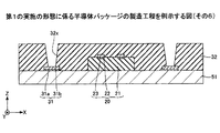
[第1の実施の形態に係る半導体パッケージの構造]
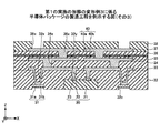
図1は、第1の実施の形態に係る半導体パッケージを例示する断面図である。図1を参照するに、半導体パッケージ10は、半導体チップ20と、第1配線層31と、第1絶縁層32と、第2配線層33と、第2絶縁層34と、第3配線層35と、第3絶縁層36と、第4配線層37と、ソルダーレジスト層38と、外部接続端子39とを有する。
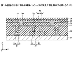
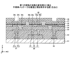
次に、第1の実施の形態に係る半導体パッケージの製造方法について説明する。図3〜図16は、第1の実施の形態に係る半導体パッケージの製造工程を例示する図である。
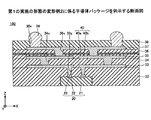
次に、第1の実施の形態に係る半導体パッケージの実装例について説明する。図17は、第1の実施の形態に係る半導体パッケージの実装例を示す断面図である。図17を参照するに、マザーボード100上に半導体パッケージ101が実装され、更に半導体パッケージ101上に半導体パッケージ102が実装されている。なお、図17では、便宜上、半導体パッケージ101及び102は別符号としているが、何れも半導体パッケージ10(図1参照)と同一構造の半導体パッケージである。又、図17において、半導体パッケージ101及び102は、図1に示す半導体パッケージ10とは上下が反転した状態で描かれている。
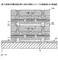
第1の実施の形態の変形例1では、第1絶縁層32(封止絶縁層)から最も遠い絶縁層にあたるソルダーレジスト層に、ガラスクロス40を内蔵する例を示す。なお、第1の実施の形態の変形例1において、既に説明した実施の形態と同一構成部品についての説明は省略する。
第1の実施の形態の変形例2では、第1電極パッド31を設けない例を示す。なお、第1の実施の形態の変形例2において、既に説明した実施の形態と同一構成部品についての説明は省略する。
第1の実施の形態の変形例3では、第1電極パッド31を第1絶縁層32の下面より窪んだ位置に設ける例を示す。なお、第1の実施の形態の変形例3において、既に説明した実施の形態と同一構成部品についての説明は省略する。
図1において第2配線層33と第2絶縁層34との間に、更に絶縁層と配線層を交互に3層ずつ挿入した、全部で7つの配線層及び7つの絶縁層(1つのソルダーレジスト層を含む)を有する半導体パッケージ(便宜上、半導体パッケージ10Dとする)について、反りのシミュレーションを実行した。

20 半導体チップ
21 半導体基板
22 電極パッド
23 突起電極
31 第1配線層
31a 第1層
31b 第2層
32 第1絶縁層
32x 第1ビアホール
32y 第2ビアホール
32z 凹部
33 第2配線層
34 第2絶縁層
34x 第3ビアホール
35 第3配線層
36、46 第3絶縁層
36x 第4ビアホール
37 第4配線層
37x 凹部
38、48 ソルダーレジスト層
38x、48x、52x 開口部
39 外部接続端子
40 ガラスクロス
40a、40b ガラス繊維束
51 支持体
52 レジスト層
53 犠牲層
100 マザーボード
110 電極パッド
Claims (10)
- 半導体チップの回路形成面及び側面を封止する封止絶縁層と、
前記封止絶縁層の前記回路形成面側の面である第1面に交互に積層された配線層及び絶縁層と、を有し、
前記第1面に形成された配線層は、前記半導体チップと電気的に接続されており、
前記絶縁層は補強部材を内蔵している半導体パッケージ。 - 前記第1面には、複数の配線層及び複数の絶縁層が交互に積層され、
前記封止絶縁層から最も遠い絶縁層は補強部材を内蔵している請求項1記載の半導体パッケージ。 - 前記第1面には、複数の配線層及び複数の絶縁層が交互に積層され、
前記封止絶縁層から最も遠い絶縁層に隣接する絶縁層は補強部材を内蔵している請求項1又は2記載の半導体パッケージ。 - 前記補強部材は織布又は不織布である請求項1乃至3の何れか一項記載の半導体パッケージ。
- 前記封止絶縁層の第1面の反対面である第2面から露出する電極パッドと、
前記封止絶縁層を貫通し、前記第1面に形成されている配線層と前記電極パッドとを電気的に接続する貫通配線と、を更に有する請求項1乃至4の何れか一項記載の半導体パッケージ。 - 前記半導体チップの裏面及び前記電極パッドの露出面は、前記第2面と面一である請求項5記載の半導体パッケージ。
- 前記半導体チップの裏面は、前記第2面と面一であり、
前記電極パッドの露出面は、前記第2面よりも窪んでいる請求項5記載の半導体パッケージ。 - 支持体の一方の面に半導体チップを回路形成面を上にして配置する第1工程と、
前記半導体チップの回路形成面及び側面を封止するように、前記支持体の一方の面に封止絶縁層を形成する第2工程と、
前記封止絶縁層の前記回路形成面側の面である第1面に、複数の配線層及び複数の絶縁層を交互に積層する第3工程と、を有し、
前記第3工程では、前記第1面に前記半導体チップと電気的に接続するように配線層を形成し、更に、少なくとも1つの絶縁層として補強部材を内蔵している絶縁層を積層する半導体パッケージの製造方法。 - 前記補強部材は織布又は不織布である請求項8記載の半導体パッケージの製造方法。
- 前記第2工程よりも前に、前記支持体の一方の面に電極パッドを形成し、
前記第2工程では、前記半導体チップの回路形成面及び側面、並びに、前記電極パッドの上面及び側面を封止するように、前記支持体の一方の面に封止絶縁層を形成し、
前記第2工程と前記第3工程との間に、前記封止絶縁層を貫通し、前記電極パッドの上面を露出する貫通孔を形成し、
前記第3工程で前記第1面に形成する配線層は、前記貫通孔内に形成され前記電極パッドと電気的に接続される貫通配線を含む請求項8又は9記載の半導体パッケージの製造方法。
Priority Applications (2)
| Application Number | Priority Date | Filing Date | Title |
|---|---|---|---|
| JP2011013180A JP5715835B2 (ja) | 2011-01-25 | 2011-01-25 | 半導体パッケージ及びその製造方法 |
| US13/354,663 US9142524B2 (en) | 2011-01-25 | 2012-01-20 | Semiconductor package and method for manufacturing semiconductor package |
Applications Claiming Priority (1)
| Application Number | Priority Date | Filing Date | Title |
|---|---|---|---|
| JP2011013180A JP5715835B2 (ja) | 2011-01-25 | 2011-01-25 | 半導体パッケージ及びその製造方法 |
Publications (3)
| Publication Number | Publication Date |
|---|---|
| JP2012156251A true JP2012156251A (ja) | 2012-08-16 |
| JP2012156251A5 JP2012156251A5 (ja) | 2013-12-26 |
| JP5715835B2 JP5715835B2 (ja) | 2015-05-13 |
Family
ID=46543582
Family Applications (1)
| Application Number | Title | Priority Date | Filing Date |
|---|---|---|---|
| JP2011013180A Active JP5715835B2 (ja) | 2011-01-25 | 2011-01-25 | 半導体パッケージ及びその製造方法 |
Country Status (2)
| Country | Link |
|---|---|
| US (1) | US9142524B2 (ja) |
| JP (1) | JP5715835B2 (ja) |
Cited By (24)
| Publication number | Priority date | Publication date | Assignee | Title |
|---|---|---|---|---|
| JP2013254918A (ja) * | 2012-06-08 | 2013-12-19 | Shinko Electric Ind Co Ltd | 半導体パッケージ及びその製造方法 |
| JP2014086598A (ja) * | 2012-10-24 | 2014-05-12 | Hitachi Chemical Co Ltd | 半導体装置の製造方法、半導体装置、及び感光性樹脂組成物 |
| US9570400B2 (en) | 2014-05-02 | 2017-02-14 | Samsung Electronics Co., Ltd. | Semiconductor package |
| JP2017103475A (ja) * | 2017-01-24 | 2017-06-08 | 信越化学工業株式会社 | 半導体装置、積層型半導体装置、及び封止後積層型半導体装置 |
| JP2017228756A (ja) * | 2016-06-20 | 2017-12-28 | サムソン エレクトロ−メカニックス カンパニーリミテッド. | ファン−アウト半導体パッケージ |
| JP2019525488A (ja) * | 2016-08-12 | 2019-09-05 | コーボ ユーエス,インコーポレイティド | 性能を向上させたウエハレベルパッケージ |
| US20200235054A1 (en) | 2019-01-23 | 2020-07-23 | Qorvo Us, Inc. | Rf devices with enhanced performance and methods of forming the same |
| JP2021044530A (ja) * | 2019-09-09 | 2021-03-18 | 日月光半導体製造股▲ふん▼有限公司 | 埋め込み部品のパッケージ構造及びその製造方法 |
| US20210296199A1 (en) | 2018-11-29 | 2021-09-23 | Qorvo Us, Inc. | Thermally enhanced semiconductor package with at least one heat extractor and process for making the same |
| US11152363B2 (en) | 2018-03-28 | 2021-10-19 | Qorvo Us, Inc. | Bulk CMOS devices with enhanced performance and methods of forming the same utilizing bulk CMOS process |
| US20220108938A1 (en) | 2019-01-23 | 2022-04-07 | Qorvo Us, Inc. | Rf devices with enhanced performance and methods of forming the same |
| US20220139862A1 (en) | 2019-01-23 | 2022-05-05 | Qorvo Us, Inc. | Rf devices with enhanced performance and methods of forming the same |
| US11387157B2 (en) | 2019-01-23 | 2022-07-12 | Qorvo Us, Inc. | RF devices with enhanced performance and methods of forming the same |
| US11646289B2 (en) | 2019-12-02 | 2023-05-09 | Qorvo Us, Inc. | RF devices with enhanced performance and methods of forming the same |
| US11923238B2 (en) | 2019-12-12 | 2024-03-05 | Qorvo Us, Inc. | Method of forming RF devices with enhanced performance including attaching a wafer to a support carrier by a bonding technique without any polymer adhesive |
| US12046483B2 (en) | 2019-01-23 | 2024-07-23 | Qorvo Us, Inc. | RF devices with enhanced performance and methods of forming the same |
| US12046505B2 (en) | 2018-04-20 | 2024-07-23 | Qorvo Us, Inc. | RF devices with enhanced performance and methods of forming the same utilizing localized SOI formation |
| US12046535B2 (en) | 2018-07-02 | 2024-07-23 | Qorvo Us, Inc. | RF devices with enhanced performance and methods of forming the same |
| US12062701B2 (en) | 2018-04-04 | 2024-08-13 | Qorvo Us, Inc. | Gallium-nitride-based module with enhanced electrical performance and process for making the same |
| US12062571B2 (en) | 2021-03-05 | 2024-08-13 | Qorvo Us, Inc. | Selective etching process for SiGe and doped epitaxial silicon |
| US12074086B2 (en) | 2019-11-01 | 2024-08-27 | Qorvo Us, Inc. | RF devices with nanotube particles for enhanced performance and methods of forming the same |
| US12125825B2 (en) | 2019-01-23 | 2024-10-22 | Qorvo Us, Inc. | RF devices with enhanced performance and methods of forming the same |
| US12129168B2 (en) | 2019-12-23 | 2024-10-29 | Qorvo Us, Inc. | Microelectronics package with vertically stacked MEMS device and controller device |
| US12482731B2 (en) | 2020-12-11 | 2025-11-25 | Qorvo Us, Inc. | Multi-level 3D stacked package and methods of forming the same |
Families Citing this family (12)
| Publication number | Priority date | Publication date | Assignee | Title |
|---|---|---|---|---|
| US20120090883A1 (en) * | 2010-10-13 | 2012-04-19 | Qualcomm Incorporated | Method and Apparatus for Improving Substrate Warpage |
| CN103730436B (zh) * | 2012-10-15 | 2016-11-16 | 景硕科技股份有限公司 | 线路载板的增层结构 |
| JP6161380B2 (ja) * | 2013-04-17 | 2017-07-12 | ルネサスエレクトロニクス株式会社 | 半導体装置の製造方法 |
| US9728498B2 (en) * | 2015-06-30 | 2017-08-08 | Taiwan Semiconductor Manufacturing Co., Ltd. | Package structure |
| US9711458B2 (en) * | 2015-11-13 | 2017-07-18 | Taiwan Semiconductor Manufacturing Company, Ltd. | Structure and formation method for chip package |
| WO2017175001A1 (en) | 2016-04-07 | 2017-10-12 | Advanced E-Textiles Ltd | Improvements relating to textiles incorporating electronic devices |
| TWI584425B (zh) * | 2016-06-27 | 2017-05-21 | 力成科技股份有限公司 | 扇出型晶圓級封裝結構 |
| JP2018018936A (ja) * | 2016-07-27 | 2018-02-01 | イビデン株式会社 | 配線基板 |
| CN110783300B (zh) * | 2018-07-26 | 2021-08-13 | 钰桥半导体股份有限公司 | 具有调节件及防裂结构的导线架衬底及其覆晶组体 |
| JP7211757B2 (ja) * | 2018-10-22 | 2023-01-24 | 新光電気工業株式会社 | 配線基板 |
| KR20220151431A (ko) | 2021-05-06 | 2022-11-15 | 삼성전기주식회사 | 인쇄회로기판 |
| CN114188290B (zh) * | 2021-12-03 | 2024-11-22 | 江苏中科智芯集成科技有限公司 | 一种降低翘曲的扇出型封装结构 |
Citations (9)
| Publication number | Priority date | Publication date | Assignee | Title |
|---|---|---|---|---|
| JP2005332887A (ja) * | 2004-05-18 | 2005-12-02 | Shinko Electric Ind Co Ltd | 多層配線の形成方法および多層配線基板の製造方法 |
| JP2006339412A (ja) * | 2005-06-02 | 2006-12-14 | Toppan Printing Co Ltd | 半導体装置基板形成用基材、及びそれを用いた半導体装置基板の製造方法、及び半導体装置基板 |
| WO2007126090A1 (ja) * | 2006-04-27 | 2007-11-08 | Nec Corporation | 回路基板、電子デバイス装置及び回路基板の製造方法 |
| JP2008257710A (ja) * | 2007-03-13 | 2008-10-23 | Semiconductor Energy Lab Co Ltd | 半導体装置及びその作製方法 |
| JP2008300854A (ja) * | 2008-07-02 | 2008-12-11 | Shinko Electric Ind Co Ltd | 半導体装置及びその製造方法 |
| JP2008306071A (ja) * | 2007-06-08 | 2008-12-18 | Nec Corp | 半導体装置及びその製造方法 |
| JP2009224739A (ja) * | 2008-03-19 | 2009-10-01 | Shinko Electric Ind Co Ltd | 多層配線基板およびその製造方法 |
| WO2010010910A1 (ja) * | 2008-07-23 | 2010-01-28 | 日本電気株式会社 | コアレス配線基板、半導体装置及びそれらの製造方法 |
| WO2010010911A1 (ja) * | 2008-07-23 | 2010-01-28 | 日本電気株式会社 | 半導体装置及びその製造方法 |
Family Cites Families (12)
| Publication number | Priority date | Publication date | Assignee | Title |
|---|---|---|---|---|
| US7202556B2 (en) * | 2001-12-20 | 2007-04-10 | Micron Technology, Inc. | Semiconductor package having substrate with multi-layer metal bumps |
| TWI239581B (en) * | 2003-01-16 | 2005-09-11 | Casio Computer Co Ltd | Semiconductor device and method of manufacturing the same |
| JP4072176B2 (ja) * | 2005-08-29 | 2008-04-09 | 新光電気工業株式会社 | 多層配線基板の製造方法 |
| DE102006062473A1 (de) * | 2006-12-28 | 2008-07-03 | Qimonda Ag | Halbleiterbauelement mit auf einem Substrat montiertem Chip |
| JP4073945B1 (ja) * | 2007-01-12 | 2008-04-09 | 新光電気工業株式会社 | 多層配線基板の製造方法 |
| JP4842167B2 (ja) * | 2007-02-07 | 2011-12-21 | 新光電気工業株式会社 | 多層配線基板の製造方法 |
| EP1970952A3 (en) * | 2007-03-13 | 2009-05-06 | Semiconductor Energy Laboratory Co., Ltd. | Semiconductor device and manufacturing method thereof |
| KR101517598B1 (ko) * | 2008-07-21 | 2015-05-06 | 삼성전자주식회사 | 반도체 장치 및 그 제조 방법 |
| WO2010024233A1 (ja) * | 2008-08-27 | 2010-03-04 | 日本電気株式会社 | 機能素子を内蔵可能な配線基板及びその製造方法 |
| JP5249173B2 (ja) * | 2009-10-30 | 2013-07-31 | 新光電気工業株式会社 | 半導体素子実装配線基板及びその製造方法 |
| JP2011187473A (ja) * | 2010-03-04 | 2011-09-22 | Nec Corp | 半導体素子内蔵配線基板 |
| JP5570855B2 (ja) * | 2010-03-18 | 2014-08-13 | 新光電気工業株式会社 | 配線基板及びその製造方法並びに半導体装置及びその製造方法 |
-
2011
- 2011-01-25 JP JP2011013180A patent/JP5715835B2/ja active Active
-
2012
- 2012-01-20 US US13/354,663 patent/US9142524B2/en active Active
Patent Citations (9)
| Publication number | Priority date | Publication date | Assignee | Title |
|---|---|---|---|---|
| JP2005332887A (ja) * | 2004-05-18 | 2005-12-02 | Shinko Electric Ind Co Ltd | 多層配線の形成方法および多層配線基板の製造方法 |
| JP2006339412A (ja) * | 2005-06-02 | 2006-12-14 | Toppan Printing Co Ltd | 半導体装置基板形成用基材、及びそれを用いた半導体装置基板の製造方法、及び半導体装置基板 |
| WO2007126090A1 (ja) * | 2006-04-27 | 2007-11-08 | Nec Corporation | 回路基板、電子デバイス装置及び回路基板の製造方法 |
| JP2008257710A (ja) * | 2007-03-13 | 2008-10-23 | Semiconductor Energy Lab Co Ltd | 半導体装置及びその作製方法 |
| JP2008306071A (ja) * | 2007-06-08 | 2008-12-18 | Nec Corp | 半導体装置及びその製造方法 |
| JP2009224739A (ja) * | 2008-03-19 | 2009-10-01 | Shinko Electric Ind Co Ltd | 多層配線基板およびその製造方法 |
| JP2008300854A (ja) * | 2008-07-02 | 2008-12-11 | Shinko Electric Ind Co Ltd | 半導体装置及びその製造方法 |
| WO2010010910A1 (ja) * | 2008-07-23 | 2010-01-28 | 日本電気株式会社 | コアレス配線基板、半導体装置及びそれらの製造方法 |
| WO2010010911A1 (ja) * | 2008-07-23 | 2010-01-28 | 日本電気株式会社 | 半導体装置及びその製造方法 |
Cited By (43)
| Publication number | Priority date | Publication date | Assignee | Title |
|---|---|---|---|---|
| JP2013254918A (ja) * | 2012-06-08 | 2013-12-19 | Shinko Electric Ind Co Ltd | 半導体パッケージ及びその製造方法 |
| JP2014086598A (ja) * | 2012-10-24 | 2014-05-12 | Hitachi Chemical Co Ltd | 半導体装置の製造方法、半導体装置、及び感光性樹脂組成物 |
| US9570400B2 (en) | 2014-05-02 | 2017-02-14 | Samsung Electronics Co., Ltd. | Semiconductor package |
| US10714437B2 (en) | 2016-06-20 | 2020-07-14 | Samsung Electronics Co., Ltd. | Fan-out semiconductor package |
| US11011482B2 (en) | 2016-06-20 | 2021-05-18 | Samsung Electronics Co., Ltd. | Fan-out semiconductor package |
| JP2017228756A (ja) * | 2016-06-20 | 2017-12-28 | サムソン エレクトロ−メカニックス カンパニーリミテッド. | ファン−アウト半導体パッケージ |
| US10600748B2 (en) | 2016-06-20 | 2020-03-24 | Samsung Electronics Co., Ltd. | Fan-out semiconductor package |
| JP2022071128A (ja) * | 2016-08-12 | 2022-05-13 | コーボ ユーエス,インコーポレイティド | 性能を向上させたウエハレベルパッケージ |
| JP2019525488A (ja) * | 2016-08-12 | 2019-09-05 | コーボ ユーエス,インコーポレイティド | 性能を向上させたウエハレベルパッケージ |
| JP7037544B2 (ja) | 2016-08-12 | 2022-03-16 | コーボ ユーエス,インコーポレイティド | 性能を向上させたウエハレベルパッケージ |
| JP7265052B2 (ja) | 2016-08-12 | 2023-04-25 | コーボ ユーエス,インコーポレイティド | 性能を向上させたウエハレベルパッケージ |
| JP2017103475A (ja) * | 2017-01-24 | 2017-06-08 | 信越化学工業株式会社 | 半導体装置、積層型半導体装置、及び封止後積層型半導体装置 |
| US11152363B2 (en) | 2018-03-28 | 2021-10-19 | Qorvo Us, Inc. | Bulk CMOS devices with enhanced performance and methods of forming the same utilizing bulk CMOS process |
| US12062701B2 (en) | 2018-04-04 | 2024-08-13 | Qorvo Us, Inc. | Gallium-nitride-based module with enhanced electrical performance and process for making the same |
| US12062700B2 (en) | 2018-04-04 | 2024-08-13 | Qorvo Us, Inc. | Gallium-nitride-based module with enhanced electrical performance and process for making the same |
| US12046505B2 (en) | 2018-04-20 | 2024-07-23 | Qorvo Us, Inc. | RF devices with enhanced performance and methods of forming the same utilizing localized SOI formation |
| US12125739B2 (en) | 2018-04-20 | 2024-10-22 | Qorvo Us, Inc. | RF devices with enhanced performance and methods of forming the same utilizing localized SOI formation |
| US12046535B2 (en) | 2018-07-02 | 2024-07-23 | Qorvo Us, Inc. | RF devices with enhanced performance and methods of forming the same |
| US12165951B2 (en) | 2018-07-02 | 2024-12-10 | Qorvo Us, Inc. | RF devices with enhanced performance and methods of forming the same |
| US11646242B2 (en) | 2018-11-29 | 2023-05-09 | Qorvo Us, Inc. | Thermally enhanced semiconductor package with at least one heat extractor and process for making the same |
| US11942389B2 (en) | 2018-11-29 | 2024-03-26 | Qorvo Us, Inc. | Thermally enhanced semiconductor package with at least one heat extractor and process for making the same |
| US20210296199A1 (en) | 2018-11-29 | 2021-09-23 | Qorvo Us, Inc. | Thermally enhanced semiconductor package with at least one heat extractor and process for making the same |
| US12057374B2 (en) | 2019-01-23 | 2024-08-06 | Qorvo Us, Inc. | RF devices with enhanced performance and methods of forming the same |
| US12112999B2 (en) | 2019-01-23 | 2024-10-08 | Qorvo Us, Inc. | RF devices with enhanced performance and methods of forming the same |
| US12368056B2 (en) | 2019-01-23 | 2025-07-22 | Qorvo Us, Inc. | RF devices with enhanced performance and methods of forming the same |
| US11961813B2 (en) | 2019-01-23 | 2024-04-16 | Qorvo Us, Inc. | RF devices with enhanced performance and methods of forming the same |
| US12046483B2 (en) | 2019-01-23 | 2024-07-23 | Qorvo Us, Inc. | RF devices with enhanced performance and methods of forming the same |
| US20220139862A1 (en) | 2019-01-23 | 2022-05-05 | Qorvo Us, Inc. | Rf devices with enhanced performance and methods of forming the same |
| US20220108938A1 (en) | 2019-01-23 | 2022-04-07 | Qorvo Us, Inc. | Rf devices with enhanced performance and methods of forming the same |
| US12046570B2 (en) | 2019-01-23 | 2024-07-23 | Qorvo Us, Inc. | RF devices with enhanced performance and methods of forming the same |
| US11387157B2 (en) | 2019-01-23 | 2022-07-12 | Qorvo Us, Inc. | RF devices with enhanced performance and methods of forming the same |
| US12062623B2 (en) | 2019-01-23 | 2024-08-13 | Qorvo Us, Inc. | RF device without silicon handle substrate for enhanced thermal and electrical performance and methods of forming the same |
| US20200235054A1 (en) | 2019-01-23 | 2020-07-23 | Qorvo Us, Inc. | Rf devices with enhanced performance and methods of forming the same |
| US11923313B2 (en) | 2019-01-23 | 2024-03-05 | Qorvo Us, Inc. | RF device without silicon handle substrate for enhanced thermal and electrical performance and methods of forming the same |
| US12125825B2 (en) | 2019-01-23 | 2024-10-22 | Qorvo Us, Inc. | RF devices with enhanced performance and methods of forming the same |
| JP2021044530A (ja) * | 2019-09-09 | 2021-03-18 | 日月光半導体製造股▲ふん▼有限公司 | 埋め込み部品のパッケージ構造及びその製造方法 |
| US11139179B2 (en) | 2019-09-09 | 2021-10-05 | Advanced Semiconductor Engineering, Inc. | Embedded component package structure and manufacturing method thereof |
| US12074086B2 (en) | 2019-11-01 | 2024-08-27 | Qorvo Us, Inc. | RF devices with nanotube particles for enhanced performance and methods of forming the same |
| US11646289B2 (en) | 2019-12-02 | 2023-05-09 | Qorvo Us, Inc. | RF devices with enhanced performance and methods of forming the same |
| US11923238B2 (en) | 2019-12-12 | 2024-03-05 | Qorvo Us, Inc. | Method of forming RF devices with enhanced performance including attaching a wafer to a support carrier by a bonding technique without any polymer adhesive |
| US12129168B2 (en) | 2019-12-23 | 2024-10-29 | Qorvo Us, Inc. | Microelectronics package with vertically stacked MEMS device and controller device |
| US12482731B2 (en) | 2020-12-11 | 2025-11-25 | Qorvo Us, Inc. | Multi-level 3D stacked package and methods of forming the same |
| US12062571B2 (en) | 2021-03-05 | 2024-08-13 | Qorvo Us, Inc. | Selective etching process for SiGe and doped epitaxial silicon |
Also Published As
| Publication number | Publication date |
|---|---|
| US20120187557A1 (en) | 2012-07-26 |
| US9142524B2 (en) | 2015-09-22 |
| JP5715835B2 (ja) | 2015-05-13 |
Similar Documents
| Publication | Publication Date | Title |
|---|---|---|
| JP5715835B2 (ja) | 半導体パッケージ及びその製造方法 | |
| JP5903337B2 (ja) | 半導体パッケージ及びその製造方法 | |
| JP5662551B1 (ja) | 配線基板、半導体装置及び配線基板の製造方法 | |
| JP6375121B2 (ja) | 配線基板、半導体装置及び配線基板の製造方法 | |
| JP5864180B2 (ja) | 半導体パッケージ及びその製造方法 | |
| KR101968957B1 (ko) | 배선 기판 및 그 제조 방법, 반도체 패키지 | |
| JP6081693B2 (ja) | 配線基板及び配線基板の製造方法 | |
| JP5977051B2 (ja) | 半導体パッケージ、半導体装置及び半導体パッケージの製造方法 | |
| JP6152254B2 (ja) | 半導体パッケージ、半導体装置及び半導体パッケージの製造方法 | |
| CN102300396B (zh) | 配线基板 | |
| JP5851211B2 (ja) | 半導体パッケージ、半導体パッケージの製造方法及び半導体装置 | |
| JP6594264B2 (ja) | 配線基板及び半導体装置、並びにそれらの製造方法 | |
| JP6133227B2 (ja) | 配線基板及びその製造方法 | |
| JP6661232B2 (ja) | 配線基板、半導体装置、配線基板の製造方法及び半導体装置の製造方法 | |
| US11152293B2 (en) | Wiring board having two insulating films and hole penetrating therethrough | |
| JP2013069807A (ja) | 半導体パッケージ及びその製造方法 | |
| JP2022016495A (ja) | 配線基板、半導体装置、配線基板の製造方法及び半導体装置の製造方法 | |
| JP6761064B2 (ja) | 配線基板及びその製造方法 | |
| CN103369874B (zh) | 布线基板的制造方法以及布线基板 | |
| JP2009081357A (ja) | 配線基板の製造方法及び配線基板 | |
| JP2014045071A (ja) | プリント配線板及びその製造方法 | |
| JP5444136B2 (ja) | 配線基板 | |
| JP5432354B2 (ja) | 配線基板製造用の仮基板及びその製造方法 | |
| JP2012004440A5 (ja) |
Legal Events
| Date | Code | Title | Description |
|---|---|---|---|
| A521 | Request for written amendment filed |
Free format text: JAPANESE INTERMEDIATE CODE: A523 Effective date: 20131107 |
|
| A621 | Written request for application examination |
Free format text: JAPANESE INTERMEDIATE CODE: A621 Effective date: 20131107 |
|
| A977 | Report on retrieval |
Free format text: JAPANESE INTERMEDIATE CODE: A971007 Effective date: 20140828 |
|
| A131 | Notification of reasons for refusal |
Free format text: JAPANESE INTERMEDIATE CODE: A131 Effective date: 20140916 |
|
| A521 | Request for written amendment filed |
Free format text: JAPANESE INTERMEDIATE CODE: A523 Effective date: 20141105 |
|
| A131 | Notification of reasons for refusal |
Free format text: JAPANESE INTERMEDIATE CODE: A131 Effective date: 20141209 |
|
| A521 | Request for written amendment filed |
Free format text: JAPANESE INTERMEDIATE CODE: A523 Effective date: 20150128 |
|
| TRDD | Decision of grant or rejection written | ||
| A01 | Written decision to grant a patent or to grant a registration (utility model) |
Free format text: JAPANESE INTERMEDIATE CODE: A01 Effective date: 20150224 |
|
| A61 | First payment of annual fees (during grant procedure) |
Free format text: JAPANESE INTERMEDIATE CODE: A61 Effective date: 20150316 |
|
| R150 | Certificate of patent or registration of utility model |
Ref document number: 5715835 Country of ref document: JP Free format text: JAPANESE INTERMEDIATE CODE: R150 |