JP2012157151A - Power supply unit and electronic apparatus using the same - Google Patents
Power supply unit and electronic apparatus using the same Download PDFInfo
- Publication number
- JP2012157151A JP2012157151A JP2011013675A JP2011013675A JP2012157151A JP 2012157151 A JP2012157151 A JP 2012157151A JP 2011013675 A JP2011013675 A JP 2011013675A JP 2011013675 A JP2011013675 A JP 2011013675A JP 2012157151 A JP2012157151 A JP 2012157151A
- Authority
- JP
- Japan
- Prior art keywords
- power supply
- supply device
- output
- control unit
- output voltage
- Prior art date
- Legal status (The legal status is an assumption and is not a legal conclusion. Google has not performed a legal analysis and makes no representation as to the accuracy of the status listed.)
- Granted
Links
- 238000001514 detection method Methods 0.000 claims description 37
- 230000007274 generation of a signal involved in cell-cell signaling Effects 0.000 claims description 6
- 239000003990 capacitor Substances 0.000 description 22
- 239000004065 semiconductor Substances 0.000 description 13
- 230000005669 field effect Effects 0.000 description 8
- 238000010586 diagram Methods 0.000 description 3
- 239000004973 liquid crystal related substance Substances 0.000 description 2
- 230000004048 modification Effects 0.000 description 2
- 238000012986 modification Methods 0.000 description 2
- 230000004913 activation Effects 0.000 description 1
- 229910044991 metal oxide Inorganic materials 0.000 description 1
- 150000004706 metal oxides Chemical class 0.000 description 1
- 230000000630 rising effect Effects 0.000 description 1
Images

Landscapes
- Direct Current Feeding And Distribution (AREA)
- Dc-Dc Converters (AREA)
Abstract
Description
本発明は、複数の出力電圧を生成する多出力型の電源装置、及び、これを用いた電子機器に関するものである。 The present invention relates to a multi-output type power supply device that generates a plurality of output voltages, and an electronic apparatus using the same.
図5は、電源装置の一従来例を示す図である。本従来例の電源装置100は、出力電圧V1を生成する第1電源部101と、出力電圧V2を生成する第2電源部102と、出力電圧V3を生成する第3電源部103と、出力電圧V4を生成する第4電源部104と、を有する多出力型の電源装置である。
FIG. 5 is a diagram illustrating a conventional example of a power supply device. The
本従来例の電源装置100には、メインコントローラ200からイネーブル信号EN1〜EN4がパラレル入力されており、電源部101〜104は、それぞれ、イネーブル信号EN1〜EN4に応じてオン/オフ制御されていた。
Enable signals EN1 to EN4 are input in parallel from the
なお、上記に関連する従来技術の一例としては、特許文献1を挙げることができる。
As an example of the related art related to the above,
ところで、多出力型の電源装置100では、システムの安全性などを鑑み、電源装置100の起動時には出力電圧の目標値がより低い電源部から順にオンしていき、逆に、電源装置100の停止時には出力電圧の目標値がより高い電源部から順にオフしていくように要求される場合があった。このような場合、メインコントローラ200では、所望のオン/オフシーケンス(電源部101〜104のオン/オフ順序)を実現するために、イネーブル信号EN1〜EN4の生成タイミングを制御しなければならず、メインコントローラ200の負荷(電源装置100が搭載されるシステム側の負荷)が増大していた。
By the way, in the multi-output type
本発明は、本願の発明者により見出された上記の問題点に鑑み、システムの負荷を低減することが可能な電源装置、及び、これを用いた電子機器を提供することを目的とする。 In view of the above-described problems found by the inventors of the present application, an object of the present invention is to provide a power supply device capable of reducing the load on the system and an electronic apparatus using the same.
上記目的を達成するために、本発明に係る電源装置は、各々別系統の出力電圧を生成する複数の電源部と、イネーブル信号の入力を受けて所定の順序で前記複数の電源部のオン/オフ制御を行うシーケンス制御部と、を有する構成(第1の構成)とされている。 In order to achieve the above object, a power supply device according to the present invention includes a plurality of power supply units each generating an output voltage of a different system, and an ON / OFF of the plurality of power supply units in a predetermined order upon receiving an enable signal. And a sequence control unit that performs off control (first configuration).
なお、上記第1の構成から成る電源装置において、前記シーケンス制御部は、前記電源装置の起動時には出力電圧の目標値がより低い電源部から順にオンしていく構成(第2の構成)にするとよい。 In the power supply device having the first configuration described above, the sequence control unit may be configured to turn on sequentially from a power supply unit having a lower output voltage target value when the power supply device is started up (second configuration). Good.
また、上記第2の構成から成る電源装置において、前記シーケンス制御部は、前記電源装置の停止時には出力電圧の目標値がより高い電源部から順にオフしていく構成(第3の構成)にするとよい。 Further, in the power supply device having the second configuration, when the power supply device is stopped, the sequence control unit is configured to be sequentially turned off from a power supply unit having a higher output voltage target value (third configuration). Good.
また、上記第3の構成から成る電源装置にて、前記シーケンス制御部は、前記電源装置の起動時には先にオンした電源部の出力電圧が立ち上がったことを検出して次にオンすべき電源部をオンし、前記電源装置の停止時には先にオフした電源部の出力電圧が立ち下がったことを検出して次にオフすべき電源部をオフする構成(第4の構成)にするとよい。 Further, in the power supply device having the third configuration, the sequence control unit detects that the output voltage of the power supply unit that has been turned on first rises when the power supply device is started up, and is to be turned on next time. When the power supply apparatus is stopped, it is preferable to detect that the output voltage of the power supply section that was turned off first falls and to turn off the power supply section that should be turned off next (fourth structure).
また、上記第4の構成から成る電源装置において、前記シーケンス制御部は、前記複数の出力電圧と各々に設定された閾値電圧とを各々比較して複数の出力検出信号を生成する出力検出信号生成部と、前記イネーブル信号と前記複数の出力検出信号から複数のオン/オフ制御信号を生成して前記複数の電源部に各々供給するオン/オフ制御信号生成部と、を含む構成(第5の構成)にするとよい。 Further, in the power supply device having the fourth configuration, the sequence control unit compares the plurality of output voltages with a threshold voltage set for each to generate a plurality of output detection signals. And an on / off control signal generation unit that generates a plurality of on / off control signals from the enable signal and the plurality of output detection signals and supplies the plurality of on / off control signals to the plurality of power supply units, Configuration).
また、上記第5の構成から成る電源装置において、前記閾値電圧には、ヒステリシスが与えられている構成(第6の構成)にするとよい。 In the power supply device having the fifth configuration, the threshold voltage may be configured to have a hysteresis (sixth configuration).
また、上記第6の構成から成る電源装置は、前記複数の出力検出信号を前記電源装置の外部に出力するための外部端子を有する構成(第7の構成)にするとよい。 The power supply device having the sixth configuration may have a configuration (seventh configuration) having an external terminal for outputting the plurality of output detection signals to the outside of the power supply device.
また、本発明に係る電子機器は、上記第1〜第7いずれかの構成から成る電源装置と、前記電源装置に前記イネーブル信号を供給するメインコントローラと、前記複数の出力電圧が供給される複数の負荷と、を有する構成(第8の構成)とされている。 According to another aspect of the present invention, there is provided an electronic apparatus including a power supply device having any one of the first to seventh configurations, a main controller that supplies the enable signal to the power supply device, and a plurality of output voltages to which the plurality of output voltages are supplied. It is set as the structure (8th structure) which has this load.
本発明によれば、システム側の負荷を低減することが可能な電源装置、及び、これを用いた電子機器を提供することが可能となる。 ADVANTAGE OF THE INVENTION According to this invention, it becomes possible to provide the power supply device which can reduce the load by the side of a system, and an electronic device using the same.
<全体構成>
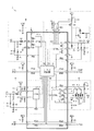
図1は、本発明に係る電源装置の一実施形態を示す図である。本実施形態の電源装置1は、回路ブロック的に見ると、第1降圧DC/DCコンバータAと、第2降圧DC/DCコンバータBと、昇圧DC/DCコンバータCと、正チャージポンプDと、シーケンス制御部Xと、を有する。
<Overall configuration>
FIG. 1 is a diagram showing an embodiment of a power supply device according to the present invention. In terms of circuit blocks, the
なお、本明細書中では、第1降圧DC/DCコンバータA、第2降圧DC/DCコンバータB、昇圧DC/DCコンバータC、及び、正チャージポンプDのことを適宜、電源部A〜Dと略称することがある。 In this specification, the first step-down DC / DC converter A, the second step-down DC / DC converter B, the step-up DC / DC converter C, and the positive charge pump D are referred to as power supply units A to D as appropriate. Sometimes abbreviated.
第1降圧DC/DCコンバータAは、電源電圧VCCを降圧して出力電圧V1を生成する降圧型のスイッチングレギュレータである。第1降圧DC/DCコンバータAは、Pチャネル型MOS[Metal Oxide Semiconductor]電界効果トランジスタA1と、Nチャネル型MOS電界効果トランジスタA2と、インダクタA3と、抵抗A4〜A8と、キャパシタA9〜A11と、スイッチ制御部A12と、を含む。 The first step-down DC / DC converter A is a step-down switching regulator that steps down the power supply voltage VCC and generates an output voltage V1. The first step-down DC / DC converter A includes a P-channel MOS [Metal Oxide Semiconductor] field effect transistor A1, an N-channel MOS field effect transistor A2, an inductor A3, resistors A4 to A8, and capacitors A9 to A11. , Switch control unit A12.
トランジスタA1のソース及びバックゲートは、いずれも電源電圧VCCの印加端に接続されている。トランジスタA1のドレインは、インダクタA3の第1端に接続されている。トランジスタA1のゲートは、スイッチ制御部A12に接続されている。トランジスタA2のソース及びバックゲートは、いずれも接地端に接続されている。トランジスタA2のドレインは、インダクタA3の第1端に接続されている。トランジスタA2のゲートは、スイッチ制御部A12に接続されている。インダクタA3の第2端は、出力電圧V1の印加端に接続されている。抵抗A4は、トランジスタA1のゲートと電源電圧VCCの印加端との間に接続されている。抵抗A5は、トランジスタA2のゲートと接地端との間に接続されている。抵抗A6と抵抗A7から成る直列回路は、出力電圧V1の印加端と接地端との間に接続されている。抵抗A6と抵抗A7との接続ノードは、帰還電圧FB1の印加端としてスイッチ制御部A12及びシーケンス制御部Xに接続されている。抵抗A8とキャパシタA9から成る直列回路は、抵抗A6の両端間に接続されている。キャパシタA10は、電源電圧VCCの印加端と接地端との間に接続されている。キャパシタA11は、出力電圧V1の印加端と接地端との間に接続されている。 The source and back gate of the transistor A1 are both connected to the application terminal of the power supply voltage VCC. The drain of the transistor A1 is connected to the first end of the inductor A3. The gate of the transistor A1 is connected to the switch control unit A12. The source and back gate of the transistor A2 are both connected to the ground terminal. The drain of the transistor A2 is connected to the first end of the inductor A3. The gate of the transistor A2 is connected to the switch control unit A12. The second end of the inductor A3 is connected to the application end of the output voltage V1. The resistor A4 is connected between the gate of the transistor A1 and the application end of the power supply voltage VCC. The resistor A5 is connected between the gate of the transistor A2 and the ground terminal. A series circuit including the resistors A6 and A7 is connected between the application terminal of the output voltage V1 and the ground terminal. A connection node between the resistor A6 and the resistor A7 is connected to the switch control unit A12 and the sequence control unit X as an application end of the feedback voltage FB1. A series circuit including a resistor A8 and a capacitor A9 is connected between both ends of the resistor A6. The capacitor A10 is connected between the application terminal of the power supply voltage VCC and the ground terminal. The capacitor A11 is connected between the application terminal of the output voltage V1 and the ground terminal.
スイッチ制御部A12は、電源電圧VCCの入力を受けて動作し、帰還電圧FB1が目標値と一致するようにトランジスタA1及びA2のスイッチング制御を行う。また、スイッチ制御部A12は、シーケンス制御部Xから入力されるオン/オフ制御信号S1に応じてオン/オフ制御される。 The switch control unit A12 operates in response to the input of the power supply voltage VCC, and performs switching control of the transistors A1 and A2 so that the feedback voltage FB1 matches the target value. The switch control unit A12 is on / off controlled according to the on / off control signal S1 input from the sequence control unit X.
なお、上記した構成要素のうち、スイッチ制御部A12は半導体装置Yに集積化されており、その他の回路素子A1〜A11はいずれも半導体装置Yに外付けされている。 Of the above-described components, the switch control unit A12 is integrated in the semiconductor device Y, and the other circuit elements A1 to A11 are all externally attached to the semiconductor device Y.
第2降圧DC/DCコンバータBは、電源電圧VCCを降圧して出力電圧V2を生成する降圧型のスイッチングレギュレータである。第2降圧DC/DCコンバータBは、Pチャネル型MOS電界効果トランジスタB1と、Nチャネル型MOS電界効果トランジスタB2と、インダクタB3と、抵抗B4〜B6と、キャパシタB7〜B9と、スイッチ制御部B10と、を含む。 The second step-down DC / DC converter B is a step-down switching regulator that steps down the power supply voltage VCC to generate the output voltage V2. The second step-down DC / DC converter B includes a P-channel MOS field effect transistor B1, an N-channel MOS field effect transistor B2, an inductor B3, resistors B4 to B6, capacitors B7 to B9, and a switch control unit B10. And including.
トランジスタB1のソース及びバックゲートは、いずれも電源電圧VCCの印加端に接続されている。トランジスタB1のドレインは、インダクタB3の第1端に接続されている。トランジスタB1のゲートは、スイッチ制御部B10に接続されている。トランジスタB2のソース及びバックゲートは、いずれも接地端に接続されている。トランジスタB2のドレインは、インダクタB3の第1端に接続されている。トランジスタB2のゲートは、スイッチ制御部B10に接続されている。インダクタB3の第2端は、出力電圧V2の印加端に接続されている。抵抗B4と抵抗B5から成る直列回路は、出力電圧V2の印加端と接地端との間に接続されている。抵抗B4と抵抗B5との接続ノードは、帰還電圧FB2の印加端としてスイッチ制御部B10及びシーケンス制御部Xに接続されている。抵抗B6とキャパシタB7から成る直列回路は、抵抗B4の両端間に接続されている。キャパシタB8は、電源電圧VCCの印加端と接地端との間に接続されている。キャパシタB9は、出力電圧V2の印加端と接地端との間に接続されている。 The source and back gate of the transistor B1 are both connected to the application terminal of the power supply voltage VCC. The drain of the transistor B1 is connected to the first end of the inductor B3. The gate of the transistor B1 is connected to the switch control unit B10. The source and back gate of the transistor B2 are both connected to the ground terminal. The drain of the transistor B2 is connected to the first end of the inductor B3. The gate of the transistor B2 is connected to the switch control unit B10. The second end of the inductor B3 is connected to the application end of the output voltage V2. The series circuit including the resistors B4 and B5 is connected between the application terminal of the output voltage V2 and the ground terminal. A connection node between the resistor B4 and the resistor B5 is connected to the switch control unit B10 and the sequence control unit X as an application terminal of the feedback voltage FB2. A series circuit including a resistor B6 and a capacitor B7 is connected between both ends of the resistor B4. The capacitor B8 is connected between the application terminal of the power supply voltage VCC and the ground terminal. The capacitor B9 is connected between the application terminal of the output voltage V2 and the ground terminal.
スイッチ制御部B10は、帰還電圧FB2が目標値と一致するようにトランジスタB1及びB2のスイッチング制御を行う。また、スイッチ制御部B10は、シーケンス制御部Xから入力されるオン/オフ制御信号S2に応じてオン/オフ制御される。 The switch control unit B10 performs switching control of the transistors B1 and B2 so that the feedback voltage FB2 matches the target value. The switch control unit B10 is on / off controlled in accordance with the on / off control signal S2 input from the sequence control unit X.
なお、上記した構成要素のうち、トランジスタB1、トランジスタB2、及び、スイッチ制御部B10はいずれも半導体装置Yに集積化されており、その他の回路素子B3〜B9はいずれも半導体装置Yに外付けされている。 Of the above-described components, the transistor B1, the transistor B2, and the switch control unit B10 are all integrated in the semiconductor device Y, and the other circuit elements B3 to B9 are all externally attached to the semiconductor device Y. Has been.
昇圧DC/DCコンバータCは、電源電圧VCCを昇圧して出力電圧V3を生成する昇圧型のスイッチングレギュレータである。昇圧DC/DCコンバータCは、Pチャネル型MOS電界効果トランジスタC0及びC1と、Nチャネル型MOS電界効果トランジスタC2と、インダクタC3と、抵抗C4〜C8と、キャパシタC9〜C12と、スイッチ制御部C13と、を含む。 The step-up DC / DC converter C is a step-up type switching regulator that steps up the power supply voltage VCC and generates an output voltage V3. The step-up DC / DC converter C includes P-channel MOS field effect transistors C0 and C1, an N-channel MOS field effect transistor C2, an inductor C3, resistors C4 to C8, capacitors C9 to C12, and a switch control unit C13. And including.
トランジスタC0のソース及びバックゲートは、いずれも抵抗C7を介して電源電圧VCCの印加端に接続される一方、スイッチ制御部C13にも接続されている。トランジスタC0のドレインは、インダクタC3の第1端に接続されている。トランジスタC0のゲートは、スイッチ制御部C13に接続されている。トランジスタC1のソース及びバックゲートは、いずれも出力電圧V3の印加端に接続されている。トランジスタC1のドレインは、インダクタC3の第2端に接続されている。トランジスタC1のゲートは、スイッチ制御部C13に接続されている。トランジスタC2のソース及びバックゲートは、いずれも接地端に接続されている。トランジスタC2のドレインは、インダクタC3の第2端に接続されている。トランジスタC2のゲートは、スイッチ制御部C13に接続されている。抵抗C4と抵抗C5から成る直列回路は、出力電圧V3の印加端と接地端との間に接続されている。抵抗C4と抵抗C5との接続ノードは、帰還電圧FB3の印加端としてスイッチ制御部C13及びシーケンス制御部Xに接続されている。抵抗C6とキャパシタC11から成る直列回路は、抵抗C4の両端間に接続されている。キャパシタC9は、電源電圧VCCの印加端と接地端との間に接続されている。キャパシタC10は、出力電圧V3の印加端と接地端との間に接続されている。抵抗C8とキャパシタC12から成る直列回路は、位相補償回路としてスイッチ制御部C13に接続されている。 The source and back gate of the transistor C0 are both connected to the application terminal of the power supply voltage VCC via the resistor C7, and are also connected to the switch control unit C13. The drain of the transistor C0 is connected to the first end of the inductor C3. The gate of the transistor C0 is connected to the switch control unit C13. The source and back gate of the transistor C1 are both connected to the application terminal for the output voltage V3. The drain of the transistor C1 is connected to the second end of the inductor C3. The gate of the transistor C1 is connected to the switch control unit C13. The source and back gate of the transistor C2 are both connected to the ground terminal. The drain of the transistor C2 is connected to the second end of the inductor C3. The gate of the transistor C2 is connected to the switch control unit C13. A series circuit composed of the resistor C4 and the resistor C5 is connected between the application terminal of the output voltage V3 and the ground terminal. A connection node between the resistor C4 and the resistor C5 is connected to the switch control unit C13 and the sequence control unit X as an application end of the feedback voltage FB3. A series circuit including a resistor C6 and a capacitor C11 is connected between both ends of the resistor C4. The capacitor C9 is connected between the application terminal of the power supply voltage VCC and the ground terminal. The capacitor C10 is connected between the application terminal of the output voltage V3 and the ground terminal. A series circuit including a resistor C8 and a capacitor C12 is connected to the switch control unit C13 as a phase compensation circuit.
スイッチ制御部C13は、帰還電圧FB3が目標値と一致するようにトランジスタC1及びC2のスイッチング制御を行う。また、スイッチ制御部C13は、シーケンス制御部Xから入力されるオン/オフ制御信号S3に応じてオン/オフ制御される。また、スイッチ制御部C13は、外部入力される動作モード選択信号SELに応じて、トランジスタC1及びC2のスイッチング制御に代えて、外付けトランジスタのスイッチング制御を行う機能を備えている(図中の括弧付き部分を参照)。また、スイッチ制御部C13は、インダクタ電流が過大となったときにトランジスタC0をオフして昇圧動作をシャットダウンする機能も備えている。 The switch control unit C13 performs switching control of the transistors C1 and C2 so that the feedback voltage FB3 matches the target value. The switch control unit C13 is on / off controlled according to the on / off control signal S3 input from the sequence control unit X. In addition, the switch control unit C13 has a function of performing switching control of external transistors in place of switching control of the transistors C1 and C2 in accordance with an operation mode selection signal SEL input externally (in parentheses in the figure). See attached part). The switch control unit C13 also has a function of turning off the transistor C0 and shutting down the boosting operation when the inductor current becomes excessive.
なお、上記した構成要素のうち、トランジスタC1、トランジスタC2、及び、スイッチ制御部C13はいずれも半導体装置Yに集積化されており、その他の回路素子C3〜C12はいずれも半導体装置Yに外付けされている。 Of the above-described components, the transistor C1, the transistor C2, and the switch control unit C13 are all integrated in the semiconductor device Y, and the other circuit elements C3 to C12 are all externally attached to the semiconductor device Y. Has been.
正チャージポンプDは、キャパシタとスイッチを組み合わせることにより、電源電圧VCCを昇圧して出力電圧V4を生成する正昇圧型のチャージポンプである。正チャージポンプDは、Pチャネル型MOS電界効果トランジスタD1及びD2と、Nチャネル型MOS電界効果トランジスタD3と、ダイオード(スイッチ)D4〜D7と、抵抗D8及びD9と、キャパシタD10〜D14と、スイッチ制御部D15と、を含む。 The positive charge pump D is a positive boost type charge pump that boosts the power supply voltage VCC to generate an output voltage V4 by combining a capacitor and a switch. The positive charge pump D includes P-channel MOS field effect transistors D1 and D2, N-channel MOS field effect transistors D3, diodes (switches) D4 to D7, resistors D8 and D9, capacitors D10 to D14, and switches And a control unit D15.
トランジスタD1のソース及びバックゲートは、いずれも出力電圧V3の印加端に接続されている。トランジスタD1のドレインは、ダイオードD4のアノードに接続されている。トランジスタD1のゲートは、スイッチ制御部D15に接続されている。トランジスタD2のソース及びバックゲートは、いずれもダイオードD4のアノードに接続されている。トランジスタD2及びD3のドレインは、いずれもキャパシタD11及びD12の第1端に接続されている。トランジスタD2及びD3のゲートは、いずれもスイッチ制御部D15に接続されている。トランジスタD3のソース及びバックゲートは、いずれも接地端に接続されている。ダイオードD4のカソードとダイオードD5のアノードは、いずれもキャパシタD11の第2端に接続されている。ダイオードD5のカソードとダイオードD6のアノードは、いずれもキャパシタD13の第1端に接続されている。キャパシタD13の第2端は、接地端に接続されている。ダイオードD6のカソードとダイオードD7のアノードは、いずれもキャパシタD12の第2端に接続されている。ダイオードD7のカソードは、出力電圧V4の印加端に接続されている。抵抗D8と抵抗D9から成る直列回路は、出力電圧V4の印加端と接地端との間に接続されている。抵抗D8と抵抗D9との接続ノードは、帰還電圧FB4の印加端としてスイッチ制御部D15及びシーケンス制御部Xに接続されている。キャパシタD10は、出力電圧V3の印加端と接地端との間に接続されている。キャパシタD14は、出力電圧V4の印加端と接地端との間に接続されている。 The source and back gate of the transistor D1 are both connected to the application terminal for the output voltage V3. The drain of the transistor D1 is connected to the anode of the diode D4. The gate of the transistor D1 is connected to the switch control unit D15. The source and back gate of the transistor D2 are both connected to the anode of the diode D4. The drains of the transistors D2 and D3 are both connected to the first ends of the capacitors D11 and D12. The gates of the transistors D2 and D3 are both connected to the switch control unit D15. The source and back gate of the transistor D3 are both connected to the ground terminal. Both the cathode of the diode D4 and the anode of the diode D5 are connected to the second end of the capacitor D11. Both the cathode of the diode D5 and the anode of the diode D6 are connected to the first terminal of the capacitor D13. A second terminal of the capacitor D13 is connected to the ground terminal. Both the cathode of the diode D6 and the anode of the diode D7 are connected to the second end of the capacitor D12. The cathode of the diode D7 is connected to the application terminal for the output voltage V4. The series circuit composed of the resistor D8 and the resistor D9 is connected between the application terminal of the output voltage V4 and the ground terminal. A connection node between the resistor D8 and the resistor D9 is connected to the switch control unit D15 and the sequence control unit X as an application end of the feedback voltage FB4. The capacitor D10 is connected between the application terminal of the output voltage V3 and the ground terminal. The capacitor D14 is connected between the application terminal of the output voltage V4 and the ground terminal.
スイッチ制御部D15は、出力電圧V3の入力を受けて動作し、帰還電圧FB4が目標値と一致するようにトランジスタD1〜D3のスイッチング制御を行う。また、スイッチ制御部D15は、シーケンス制御部Xから入力されるオン/オフ制御信号S4に応じてオン/オフ制御される。 The switch control unit D15 operates in response to the input of the output voltage V3, and performs switching control of the transistors D1 to D3 so that the feedback voltage FB4 matches the target value. The switch control unit D15 is on / off controlled in accordance with the on / off control signal S4 input from the sequence control unit X.
なお、上記した構成要素のうち、トランジスタD1〜D3、及び、スイッチ制御部D15はいずれも半導体装置Yに集積化されており、その他の回路素子D4〜D14はいずれも半導体装置Yに外付けされている。 Of the above-described components, the transistors D1 to D3 and the switch control unit D15 are all integrated in the semiconductor device Y, and the other circuit elements D4 to D14 are all externally attached to the semiconductor device Y. ing.
シーケンス制御部Xは、半導体装置Yに集積化されており、電源装置1の外部に設けられたメインコントローラ(不図示)からイネーブル信号E1の入力を受けて先述のオン/オフ制御信号S1〜S4を生成し、所定の順序で電源部A〜Dのオン/オフ制御を行う。
The sequence control unit X is integrated in the semiconductor device Y and receives the enable signal E1 from a main controller (not shown) provided outside the
具体的に述べると、シーケンス制御部Xは、電源装置1の起動時には出力電圧の目標値がより低い電源部から順にオンしていくようにオン/オフ制御信号S1〜S4を生成し、逆に、電源装置1の停止時には出力電圧の目標値がより高い電源部から順にオフしていくようにオン/オフ制御信号S1〜S4を生成する。すなわち、V1(目標値)<V2(目標値)<V3(目標値)<V4(目標値)である場合、シーケンス制御部Xは、電源装置1の起動時には、第1降圧DC/DCコンバータA、第2降圧DC/DCコンバータB、昇圧DC/DCコンバータC、正チャージポンプDの順にオンしていくようにオン/オフ制御信号S1〜S4を生成し、逆に、電源装置1の停止時には、正チャージポンプD、昇圧DC/DCコンバータC、第2降圧DC/DCコンバータB、第1降圧DC/DCコンバータAの順にオフしていくようにオン/オフ制御信号S1〜S4を生成する。
Specifically, the sequence control unit X generates the on / off control signals S1 to S4 so that the
また、シーケンス制御部Xは、出力電圧V1〜V4と各々に設定された閾値電圧とを各々比較して出力検出信号PG1〜PG4を生成し、外部端子を介して電源装置1の外部に出力する。なお、出力検出信号PG1〜PG4が伝達される信号線は、それぞれ、外付けの抵抗R1〜R4を介して定電圧REGの印加端にプルアップされている。上記の出力検出信号PG1〜PG4は、電源装置1の外部において出力電圧V1〜V4の立ち上がり/立ち下がりが正しく完了したことを確認する際に用いられる一方、シーケンス制御部Xの内部において先述のオン/オフ制御信号S1〜S4を生成する際にも用いられる。
Further, the sequence control unit X generates output detection signals PG1 to PG4 by comparing the output voltages V1 to V4 with the threshold voltages set for each, and outputs the output detection signals PG1 to PG4 to the outside of the
なお、図1では、半導体装置Yの外部に出力された出力検出信号PG1〜PG3をイネーブル信号EN2〜EN4として半導体装置Yの内部に再入力する構成が描写されているが、本発明の構成はこれに限定されるものではなく、シーケンス制御部Xの内部で出力検出信号PG1〜PG3をイネーブル信号EN2〜EN4として読み替える構成としても構わない。後者の構成を採用した場合、イネーブル信号EN2〜EN4を入力するための外部端子は不要となるので、半導体装置Yのサイズを小型化することが可能となる。また、いずれの構成を採用した場合でも、電源装置1の外部(メインコントローラ)から供給する必要があるのは、一系統のイネーブル信号EN1のみである。 In FIG. 1, the configuration in which the output detection signals PG1 to PG3 output to the outside of the semiconductor device Y are re-input into the semiconductor device Y as enable signals EN2 to EN4 is depicted. The present invention is not limited to this, and the configuration may be such that the output detection signals PG1 to PG3 are read as enable signals EN2 to EN4 inside the sequence control unit X. When the latter configuration is adopted, the external terminals for inputting the enable signals EN2 to EN4 are not necessary, and the size of the semiconductor device Y can be reduced. In any case, only one system of the enable signal EN1 needs to be supplied from the outside of the power supply device 1 (main controller).
<シーケンス制御部>
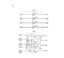
図2は、シーケンス制御部Xの一構成例を示す図である。本構成例のシーケンス制御部Xは、出力検出信号生成部X10と、オン/オフ制御信号生成部X20と、を含む。
<Sequence control unit>
FIG. 2 is a diagram illustrating a configuration example of the sequence control unit X. The sequence control unit X of this configuration example includes an output detection signal generation unit X10 and an on / off control signal generation unit X20.
出力検出信号生成部X10は、帰還電圧FB1〜FB4(出力電圧V1〜V4の分圧電圧)と各々に設定された閾値電圧とを各々比較して出力検出信号PG1〜PG4を生成する回路ブロックであり、4系統のシュミットトリガX11〜X14を含む。なお、シュミットトリガX11〜X14の各閾値電圧には、所定のヒステリシスが与えられている。このような構成とすることにより、ノイズに対する耐性を高めることが可能となる。 The output detection signal generation unit X10 is a circuit block that generates the output detection signals PG1 to PG4 by comparing the feedback voltages FB1 to FB4 (divided voltages of the output voltages V1 to V4) with the threshold voltages set for each. Yes, including 4 Schmitt triggers X11-X14. A predetermined hysteresis is given to each threshold voltage of the Schmitt triggers X11 to X14. By adopting such a configuration, it is possible to increase resistance to noise.
オン/オフ制御信号生成部X20は、イネーブル信号EN1と出力検出信号PG1〜PG4からオン/オフ制御信号S1〜S4を生成する回路ブロックであり、ORゲートX21〜X23と、ANDゲートX24〜X26とを含む。ORゲートX21は、イネーブル信号EN1と出力検出信号PG2(=イネーブル信号EN3)との論理和演算を行う。ORゲートX21の出力信号は、オン/オフ制御信号S1として出力される。ORゲートX22は、イネーブル信号EN1と出力検出信号PG3(=イネーブル信号EN4)との論理和演算を行う。ORゲートX23は、イネーブル信号EN1と出力検出信号PG4との論理和演算を行う。ANDゲートX24は、イネーブル信号EN1と出力検出信号PG3(=イネーブル信号EN4)との論理積演算を行う。ANDゲートX24の出力信号はオン/オフ制御信号S4として出力される。ANDゲートX25は、ORゲートX22の出力信号と出力検出信号PG1(=イネーブル信号EN2)との論理積演算を行う。ANDゲートX25の出力信号は、オン/オフ制御信号S2として出力される。ANDゲートX26は、ORゲートX23の出力信号と出力検出信号PG2(=イネーブル信号EN3)との論理積演算を行う。ANDゲートX26の出力信号は、オン/オフ制御信号S3として出力される。 The on / off control signal generator X20 is a circuit block that generates the on / off control signals S1 to S4 from the enable signal EN1 and the output detection signals PG1 to PG4. including. The OR gate X21 performs an OR operation between the enable signal EN1 and the output detection signal PG2 (= enable signal EN3). The output signal of the OR gate X21 is output as the on / off control signal S1. The OR gate X22 performs an OR operation between the enable signal EN1 and the output detection signal PG3 (= enable signal EN4). The OR gate X23 performs an OR operation between the enable signal EN1 and the output detection signal PG4. The AND gate X24 performs an AND operation between the enable signal EN1 and the output detection signal PG3 (= enable signal EN4). The output signal of the AND gate X24 is output as an on / off control signal S4. The AND gate X25 performs an AND operation between the output signal of the OR gate X22 and the output detection signal PG1 (= enable signal EN2). The output signal of the AND gate X25 is output as the on / off control signal S2. The AND gate X26 performs an AND operation between the output signal of the OR gate X23 and the output detection signal PG2 (= enable signal EN3). The output signal of the AND gate X26 is output as an on / off control signal S3.
<タイムチャート>
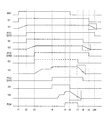
図3は、シーケンス制御部Xの一動作例を示すタイムチャートであり、上から順に、イネーブル信号EN1、オン/オフ制御信号S1、出力電圧V1、出力検出信号PG1(=イネーブル信号EN2)、オン/オフ制御信号S2、出力電圧V2、出力検出信号PG2(=イネーブル信号EN3)、オン/オフ制御信号S3、出力電圧V3、出力検出信号PG3(=イネーブル信号EN4)、オン/オフ制御信号S4、出力電圧V4、及び、出力検出信号PG4が描写されている。
<Time chart>
FIG. 3 is a time chart showing an operation example of the sequence control unit X. From the top, the enable signal EN1, the on / off control signal S1, the output voltage V1, the output detection signal PG1 (= enable signal EN2), and on / Off control signal S2, output voltage V2, output detection signal PG2 (= enable signal EN3), on / off control signal S3, output voltage V3, output detection signal PG3 (= enable signal EN4), on / off control signal S4, The output voltage V4 and the output detection signal PG4 are depicted.
時刻t1において、イネーブル信号EN1がローレベルからハイレベルに立ち上げられると、オン/オフ制御信号S1がローレベルからハイレベルに立ち上げられる。その結果第1降圧DC/DCコンバータAが起動されて出力電圧V1が上昇し始める。 When the enable signal EN1 is raised from the low level to the high level at time t1, the on / off control signal S1 is raised from the low level to the high level. As a result, the first step-down DC / DC converter A is activated and the output voltage V1 starts to rise.
時刻t2において、出力電圧V1が所定の閾値電圧を上回り、出力検出信号PG1がローレベルからハイレベルに立ち上げられると、オン/オフ制御信号S2がローレベルからハイレベルに立ち上げられる。その結果、第2降圧DC/DCコンバータBが起動されて出力電圧V2が上昇し始める。 At time t2, when the output voltage V1 exceeds a predetermined threshold voltage and the output detection signal PG1 is raised from the low level to the high level, the on / off control signal S2 is raised from the low level to the high level. As a result, the second step-down DC / DC converter B is activated and the output voltage V2 starts to rise.
時刻t3において、出力電圧V2が所定の閾値電圧を上回り、出力検出信号PG2がローレベルからハイレベルに立ち上げられると、オン/オフ制御信号S3がローレベルからハイレベルに立ち上げられる。その結果、昇圧DC/DCコンバータCが起動されて出力電圧V3が上昇し始める。 At time t3, when the output voltage V2 exceeds a predetermined threshold voltage and the output detection signal PG2 is raised from the low level to the high level, the on / off control signal S3 is raised from the low level to the high level. As a result, the step-up DC / DC converter C is activated and the output voltage V3 starts to rise.
時刻t4において、出力電圧V3が所定の閾値電圧を上回り、出力検出信号PG3がローレベルからハイレベルに立ち上げられると、オン/オフ制御信号S4がローレベルからハイレベルに立ち上げられる。その結果、正チャージポンプDが起動されて出力電圧V4が上昇し始める。 At time t4, when the output voltage V3 exceeds a predetermined threshold voltage and the output detection signal PG3 is raised from the low level to the high level, the on / off control signal S4 is raised from the low level to the high level. As a result, the positive charge pump D is activated and the output voltage V4 starts to rise.
時刻t5において、出力電圧V4が所定の閾値電圧を上回り、出力検出信号PG4がローレベルからハイレベルに立ち上げられる。この時点で、電源部A〜Dの起動が全て完了されたことになる。 At time t5, the output voltage V4 exceeds a predetermined threshold voltage, and the output detection signal PG4 is raised from the low level to the high level. At this point, the activation of the power supply units A to D is completed.
時刻t6において、イネーブル信号EN1がハイレベルからローレベルに立ち下げられると、オン/オフ制御信号S4がハイレベルからローレベルに立ち下げられる。その結果正チャージポンプDが停止されて出力電圧V4が低下し始める。 When the enable signal EN1 falls from the high level to the low level at time t6, the on / off control signal S4 falls from the high level to the low level. As a result, the positive charge pump D is stopped and the output voltage V4 starts to decrease.
時刻t7において、出力電圧V4が所定の閾値電圧を下回り、出力検出信号PG4がハイレベルからローレベルに立ち下げられると、オン/オフ制御信号S3がハイレベルからローレベルに立ち下げられる。その結果、昇圧DC/DCコンバータCが停止されて出力電圧V3が低下し始める。 At time t7, when the output voltage V4 falls below a predetermined threshold voltage and the output detection signal PG4 falls from the high level to the low level, the on / off control signal S3 falls from the high level to the low level. As a result, the step-up DC / DC converter C is stopped and the output voltage V3 starts to decrease.
時刻t8において、出力電圧V3が所定の閾値電圧を下回り、出力検出信号PG3がハイレベルからローレベルに立ち下げられると、オン/オフ制御信号S2がハイレベルからローレベルに立ち下げられる。その結果、第2降圧DC/DCコンバータBが停止されて出力電圧V2が低下し始める。 At time t8, when the output voltage V3 falls below a predetermined threshold voltage and the output detection signal PG3 falls from the high level to the low level, the on / off control signal S2 falls from the high level to the low level. As a result, the second step-down DC / DC converter B is stopped and the output voltage V2 starts to decrease.
時刻t9において、出力電圧V2が所定の閾値電圧を下回り、出力検出信号PG2がハイレベルからローレベルに立ち下げられると、オン/オフ制御信号S1がハイレベルからローレベルに立ち下げられる。その結果、第1降圧DC/DCコンバータAが停止されて出力電圧V1が低下し始める。 At time t9, when the output voltage V2 falls below a predetermined threshold voltage and the output detection signal PG2 falls from the high level to the low level, the on / off control signal S1 falls from the high level to the low level. As a result, the first step-down DC / DC converter A is stopped and the output voltage V1 starts to decrease.
時刻t10において、出力電圧V1が所定の閾値電圧を下回り、出力検出信号PG1がハイレベルからローレベルに立ち下げられる。この時点で、電源部A〜Dの停止が全て完了されたことになる。 At time t10, the output voltage V1 falls below a predetermined threshold voltage, and the output detection signal PG1 falls from the high level to the low level. At this point, the power supply units A to D are all stopped.
上記したように、シーケンス制御部Xは、電源装置1の起動時には出力電圧の目標値がより低い電源部から順にオンしていくようにオン/オフ制御信号S1〜S4を生成し、逆に、電源装置1の停止時には出力電圧の目標値がより高い電源部から順にオフしていくようにオン/オフ制御信号S1〜S4を生成する。このような構成とすることにより、システムの安全性を高めることが可能となる。
As described above, the sequence control unit X generates the on / off control signals S1 to S4 so that the
また、電源装置1が搭載されるシステム全体を見た場合、上記のオン/オフシーケンスを実現するに際して、電源装置1の外部(メインコントローラ)から供給する必要があるのは、一系統のイネーブル信号EN1のみである。従って、メインコントローラの負荷軽減やシステムの省スペース化に貢献することが可能となる。
Further, when looking at the entire system in which the
また、シーケンス制御部Xは、電源装置1の起動時には先にオンした電源部の出力電圧が立ち上がったことを検出して次にオンすべき電源部をオンし、電源装置1の停止時には先にオフした電源部の出力電圧が立ち下がったことを検出して次にオフすべき電源部をオフする構成とされている。このような構成とすることにより、オン/オフシーケンスの確実性を高めることが可能となる。
Further, the sequence control unit X detects that the output voltage of the power supply unit that was turned on first rises when the
<その他の変形例>
なお、上記の実施形態では、4チャンネルの電源部を備えた電源装置に本発明を適用した構成を例に挙げて説明を行ったが、出力チャンネル数は上記の実施形態に限定されるものではなく、複数の出力電圧を生成する多出力型の電源装置全般に広く適用することが可能である。
<Other variations>
In the embodiment described above, the configuration in which the present invention is applied to a power supply device including a 4-channel power supply unit has been described as an example. However, the number of output channels is not limited to the above embodiment. In addition, the present invention can be widely applied to all multi-output power supply devices that generate a plurality of output voltages.
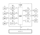
例えば、図4では、負荷3a〜3gにそれぞれ別系統の出力電圧V1〜V7を供給する7チャンネルの電源部A〜G(第1降圧DC/DCコンバータA、第2降圧DC/DCコンバータB、昇圧DC/DCコンバータC、正チャージポンプD、負チャージポンプE、コモン電圧生成部F、及び、高電圧LDO[Low Drop-Out]レギュレータG)を備えた電源装置1(液晶パネル向けのシステム電源IC)が描写されている。このような多チャンネルの電源装置1において、メインコントローラ2からイネーブル信号EN1のみの入力を受けて所定の順序で電源部A〜Gのオン/オフ制御を行うシーケンス制御部Xを設ければ、メインコントローラ2の負荷(電源装置1が搭載されるシステム側の負荷)を大幅に低減することが可能となる。
For example, in FIG. 4, seven-channel power supply units A to G (first step-down DC / DC converter A, second step-down DC / DC converter B, and the like) that supply output voltages V1 to V7 of different systems to
また、本発明の構成は、上記実施形態のほか、発明の主旨を逸脱しない範囲で種々の変更を加えることが可能である。すなわち、上記実施形態は、全ての点で例示であって、制限的なものではないと考えられるべきであり、本発明の技術的範囲は、上記実施形態の説明ではなく、特許請求の範囲によって示されるものであり、特許請求の範囲と均等の意味及び範囲内に属する全ての変更が含まれると理解されるべきである。 The configuration of the present invention can be variously modified within the scope of the present invention in addition to the above embodiment. That is, the above-described embodiment is an example in all respects and should not be considered as limiting, and the technical scope of the present invention is not the description of the above-described embodiment, but the claims. It should be understood that all modifications that come within the meaning and range of equivalents of the claims are included.
例えば、上記実施形態では、全ての電源部毎にオン/オフタイミングが異なる場合を例に挙げて説明を行ったが、本発明の構成はこれに限定されるものではなく、複数の電源部のうち、オン/オフタイミングが一致しているものがあっても構わない。 For example, in the above embodiment, the case where the on / off timing is different for every power supply unit has been described as an example. However, the configuration of the present invention is not limited to this, and a plurality of power supply units Of these, there may be ones with the same on / off timing.
また、上記実施形態では、電源装置の起動時には出力電圧の目標値がより低い電源部から順にオンしていき、電源装置の停止時には出力電圧の目標値がより高い電源部から順にオフしていく構成を例に挙げて説明を行ったが、本発明の構成はこれに限定されるものではなく、上記以外のオン/オフシーケンスとしても構わない。 In the above embodiment, the power supply device is turned on in order from the power supply unit with the lower target value of the output voltage when starting up, and the power supply unit is turned off in turn from the power supply unit with the higher target value of output voltage when the power supply device is stopped. The configuration has been described as an example, but the configuration of the present invention is not limited to this, and an on / off sequence other than the above may be used.
本発明に係る多出力型の電源装置は、例えば、液晶パネル向けのシステム電源ICとして利用することが可能である。 The multi-output type power supply device according to the present invention can be used as, for example, a system power supply IC for a liquid crystal panel.
1 電源装置
2 メインコントローラ
3a〜3g 負荷
A 第1降圧DC/DCコンバータ
B 第2降圧DC/DCコンバータ
C 昇圧DC/DCコンバータ
D 正チャージポンプ
E 負チャージポンプ
F コモン電圧生成部
G 高電圧LDOレギュレータ
X シーケンス制御部
X10 出力検出信号生成部
X20 オン/オフ制御信号生成部
DESCRIPTION OF
Claims (8)
イネーブル信号の入力を受けて所定の順序で前記複数の電源部のオン/オフ制御を行うシーケンス制御部と、
を有することを特徴とする電源装置。 A plurality of power supply units each generating an output voltage of a separate system;
A sequence control unit that receives input of an enable signal and performs on / off control of the plurality of power supply units in a predetermined order;
A power supply device comprising:
前記複数の出力電圧と各々に設定された閾値電圧とを各々比較して複数の出力検出信号を生成する出力検出信号生成部と、
前記イネーブル信号と前記複数の出力検出信号から複数のオン/オフ制御信号を生成して前記複数の電源部に各々供給するオン/オフ制御信号生成部と、
を含むことを特徴とする請求項4に記載の電源装置。 The sequence controller is
An output detection signal generation unit that generates a plurality of output detection signals by comparing the plurality of output voltages with a threshold voltage set for each of the plurality of output voltages;
An on / off control signal generation unit that generates a plurality of on / off control signals from the enable signal and the plurality of output detection signals and supplies the plurality of on / off control signals to the plurality of power supply units;
The power supply device according to claim 4, comprising:
前記電源装置に前記イネーブル信号を供給するメインコントローラと、
前記複数の出力電圧が供給される複数の負荷と、
を有することを特徴とする電子機器。 The power supply device according to any one of claims 1 to 7,
A main controller for supplying the enable signal to the power supply;
A plurality of loads to which the plurality of output voltages are supplied;
An electronic device comprising:
Priority Applications (1)
| Application Number | Priority Date | Filing Date | Title |
|---|---|---|---|
| JP2011013675A JP5695918B2 (en) | 2011-01-26 | 2011-01-26 | Power supply device and electronic device using the same |
Applications Claiming Priority (1)
| Application Number | Priority Date | Filing Date | Title |
|---|---|---|---|
| JP2011013675A JP5695918B2 (en) | 2011-01-26 | 2011-01-26 | Power supply device and electronic device using the same |
Publications (2)
| Publication Number | Publication Date |
|---|---|
| JP2012157151A true JP2012157151A (en) | 2012-08-16 |
| JP5695918B2 JP5695918B2 (en) | 2015-04-08 |
Family
ID=46838272
Family Applications (1)
| Application Number | Title | Priority Date | Filing Date |
|---|---|---|---|
| JP2011013675A Expired - Fee Related JP5695918B2 (en) | 2011-01-26 | 2011-01-26 | Power supply device and electronic device using the same |
Country Status (1)
| Country | Link |
|---|---|
| JP (1) | JP5695918B2 (en) |
Cited By (3)
| Publication number | Priority date | Publication date | Assignee | Title |
|---|---|---|---|---|
| JP2019134500A (en) * | 2018-01-29 | 2019-08-08 | ファナック株式会社 | Power supply controller and control method of the same |
| CN111697791A (en) * | 2020-06-22 | 2020-09-22 | 上海大因多媒体技术有限公司 | Centralized power supply device |
| JP2021093842A (en) * | 2019-12-10 | 2021-06-17 | ローム株式会社 | Power supply device |
Citations (6)
| Publication number | Priority date | Publication date | Assignee | Title |
|---|---|---|---|---|
| JPH0383445U (en) * | 1989-12-14 | 1991-08-26 | ||
| JP2000152497A (en) * | 1998-11-05 | 2000-05-30 | Hitachi Ltd | Power sequence circuit device |
| JP2004140944A (en) * | 2002-10-18 | 2004-05-13 | Hitachi Ltd | Power supply |
| JP2006311748A (en) * | 2005-04-28 | 2006-11-09 | Canon Inc | Power supply and equipment |
| JP2009296852A (en) * | 2008-06-09 | 2009-12-17 | Canon Inc | Power supply unit |
| JP2010170341A (en) * | 2009-01-22 | 2010-08-05 | Fujitsu Ltd | Power supply control device and power supply control system |
-
2011
- 2011-01-26 JP JP2011013675A patent/JP5695918B2/en not_active Expired - Fee Related
Patent Citations (6)
| Publication number | Priority date | Publication date | Assignee | Title |
|---|---|---|---|---|
| JPH0383445U (en) * | 1989-12-14 | 1991-08-26 | ||
| JP2000152497A (en) * | 1998-11-05 | 2000-05-30 | Hitachi Ltd | Power sequence circuit device |
| JP2004140944A (en) * | 2002-10-18 | 2004-05-13 | Hitachi Ltd | Power supply |
| JP2006311748A (en) * | 2005-04-28 | 2006-11-09 | Canon Inc | Power supply and equipment |
| JP2009296852A (en) * | 2008-06-09 | 2009-12-17 | Canon Inc | Power supply unit |
| JP2010170341A (en) * | 2009-01-22 | 2010-08-05 | Fujitsu Ltd | Power supply control device and power supply control system |
Cited By (4)
| Publication number | Priority date | Publication date | Assignee | Title |
|---|---|---|---|---|
| JP2019134500A (en) * | 2018-01-29 | 2019-08-08 | ファナック株式会社 | Power supply controller and control method of the same |
| US10720844B2 (en) | 2018-01-29 | 2020-07-21 | Fanuc Corporation | Power supply control device and control method for power supply control device |
| JP2021093842A (en) * | 2019-12-10 | 2021-06-17 | ローム株式会社 | Power supply device |
| CN111697791A (en) * | 2020-06-22 | 2020-09-22 | 上海大因多媒体技术有限公司 | Centralized power supply device |
Also Published As
| Publication number | Publication date |
|---|---|
| JP5695918B2 (en) | 2015-04-08 |
Similar Documents
| Publication | Publication Date | Title |
|---|---|---|
| JP6002818B2 (en) | Power supply | |
| US20110274295A1 (en) | Negative-voltage charge pump circuit | |
| JP4652918B2 (en) | STEP-UP SWITCHING REGULATOR, ITS CONTROL CIRCUIT, AND ELECTRONIC DEVICE USING THE SAME | |
| US20090295340A1 (en) | Regulator with soft-start using current source | |
| US20140253019A1 (en) | Charger Circuit and Control Circuit and Control Method Thereof | |
| JP6093144B2 (en) | Switching power supply | |
| JP2015130744A (en) | Power circuit | |
| JP5091101B2 (en) | Soft start circuit and power supply circuit including the soft start circuit | |
| US7336057B2 (en) | DC/DC converter | |
| JP2015058826A (en) | Power supply device | |
| JP6205596B2 (en) | Soft start circuit and power supply device | |
| JP5695918B2 (en) | Power supply device and electronic device using the same | |
| US9800149B2 (en) | Switching regulator | |
| JP6029062B2 (en) | Switching power supply | |
| US8436681B2 (en) | Voltage regulation circuit | |
| JP6693385B2 (en) | DC-DC converter and electronic control device | |
| US8912782B2 (en) | DC-to-DC converter | |
| JP2010081748A (en) | Circuit and method for controlling step-up dc-dc converter and step-up dc-dc converter | |
| JP2012039823A (en) | Control circuit for switching regulator, and switching regulator and electronic apparatus using the same | |
| US20240380306A1 (en) | Power supply control circuit and power supply device including same | |
| US20240380312A1 (en) | Power supply control circuit and power supply device including same | |
| JP2008257493A (en) | Power supply device and electric equipment using this | |
| JP5212494B2 (en) | Multiple voltage output power supply | |
| JP2014057476A (en) | Switching regulator and its control circuit, and electronic apparatus | |
| JP5086843B2 (en) | Power supply circuit device and electronic device |
Legal Events
| Date | Code | Title | Description |
|---|---|---|---|
| A621 | Written request for application examination |
Free format text: JAPANESE INTERMEDIATE CODE: A621 Effective date: 20140127 |
|
| A977 | Report on retrieval |
Free format text: JAPANESE INTERMEDIATE CODE: A971007 Effective date: 20140926 |
|
| A131 | Notification of reasons for refusal |
Free format text: JAPANESE INTERMEDIATE CODE: A131 Effective date: 20140930 |
|
| A521 | Written amendment |
Free format text: JAPANESE INTERMEDIATE CODE: A523 Effective date: 20141114 |
|
| RD03 | Notification of appointment of power of attorney |
Free format text: JAPANESE INTERMEDIATE CODE: A7423 Effective date: 20141114 |
|
| TRDD | Decision of grant or rejection written | ||
| A01 | Written decision to grant a patent or to grant a registration (utility model) |
Free format text: JAPANESE INTERMEDIATE CODE: A01 Effective date: 20150113 |
|
| A61 | First payment of annual fees (during grant procedure) |
Free format text: JAPANESE INTERMEDIATE CODE: A61 Effective date: 20150209 |
|
| R150 | Certificate of patent or registration of utility model |
Ref document number: 5695918 Country of ref document: JP Free format text: JAPANESE INTERMEDIATE CODE: R150 |
|
| LAPS | Cancellation because of no payment of annual fees |