JP2012157151A - 電源装置及びこれを用いた電子機器 - Google Patents
電源装置及びこれを用いた電子機器 Download PDFInfo
- Publication number
- JP2012157151A JP2012157151A JP2011013675A JP2011013675A JP2012157151A JP 2012157151 A JP2012157151 A JP 2012157151A JP 2011013675 A JP2011013675 A JP 2011013675A JP 2011013675 A JP2011013675 A JP 2011013675A JP 2012157151 A JP2012157151 A JP 2012157151A
- Authority
- JP
- Japan
- Prior art keywords
- power supply
- supply device
- output
- control unit
- output voltage
- Prior art date
- Legal status (The legal status is an assumption and is not a legal conclusion. Google has not performed a legal analysis and makes no representation as to the accuracy of the status listed.)
- Granted
Links
- 238000001514 detection method Methods 0.000 claims description 37
- 230000007274 generation of a signal involved in cell-cell signaling Effects 0.000 claims description 6
- 239000003990 capacitor Substances 0.000 description 22
- 239000004065 semiconductor Substances 0.000 description 13
- 230000005669 field effect Effects 0.000 description 8
- 238000010586 diagram Methods 0.000 description 3
- 239000004973 liquid crystal related substance Substances 0.000 description 2
- 230000004048 modification Effects 0.000 description 2
- 238000012986 modification Methods 0.000 description 2
- 230000004913 activation Effects 0.000 description 1
- 229910044991 metal oxide Inorganic materials 0.000 description 1
- 150000004706 metal oxides Chemical class 0.000 description 1
- 230000000630 rising effect Effects 0.000 description 1
Images

Landscapes
- Direct Current Feeding And Distribution (AREA)
- Dc-Dc Converters (AREA)
Abstract
【解決手段】各々別系統の出力電圧V1〜V7を生成する複数の電源部A〜Gと、イネーブル信号EN1の入力を受けて所定の順序で複数の電源部A〜Gのオン/オフ制御を行うシーケンス制御部Xと、を有する。
【選択図】図4
Description
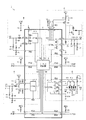
図1は、本発明に係る電源装置の一実施形態を示す図である。本実施形態の電源装置1は、回路ブロック的に見ると、第1降圧DC/DCコンバータAと、第2降圧DC/DCコンバータBと、昇圧DC/DCコンバータCと、正チャージポンプDと、シーケンス制御部Xと、を有する。
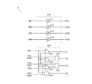
図2は、シーケンス制御部Xの一構成例を示す図である。本構成例のシーケンス制御部Xは、出力検出信号生成部X10と、オン/オフ制御信号生成部X20と、を含む。
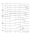
図3は、シーケンス制御部Xの一動作例を示すタイムチャートであり、上から順に、イネーブル信号EN1、オン/オフ制御信号S1、出力電圧V1、出力検出信号PG1(=イネーブル信号EN2)、オン/オフ制御信号S2、出力電圧V2、出力検出信号PG2(=イネーブル信号EN3)、オン/オフ制御信号S3、出力電圧V3、出力検出信号PG3(=イネーブル信号EN4)、オン/オフ制御信号S4、出力電圧V4、及び、出力検出信号PG4が描写されている。
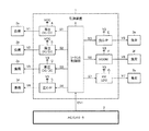
なお、上記の実施形態では、4チャンネルの電源部を備えた電源装置に本発明を適用した構成を例に挙げて説明を行ったが、出力チャンネル数は上記の実施形態に限定されるものではなく、複数の出力電圧を生成する多出力型の電源装置全般に広く適用することが可能である。
2 メインコントローラ
3a〜3g 負荷
A 第1降圧DC/DCコンバータ
B 第2降圧DC/DCコンバータ
C 昇圧DC/DCコンバータ
D 正チャージポンプ
E 負チャージポンプ
F コモン電圧生成部
G 高電圧LDOレギュレータ
X シーケンス制御部
X10 出力検出信号生成部
X20 オン/オフ制御信号生成部
Claims (8)
- 各々別系統の出力電圧を生成する複数の電源部と、
イネーブル信号の入力を受けて所定の順序で前記複数の電源部のオン/オフ制御を行うシーケンス制御部と、
を有することを特徴とする電源装置。 - 前記シーケンス制御部は、前記電源装置の起動時には出力電圧の目標値がより低い電源部から順にオンしていくことを特徴とする請求項1に記載の電源装置。
- 前記シーケンス制御部は、前記電源装置の停止時には出力電圧の目標値がより高い電源部から順にオフしていくことを特徴とする請求項2に記載の電源装置。
- 前記シーケンス制御部は、前記電源装置の起動時には先にオンした電源部の出力電圧が立ち上がったことを検出して次にオンすべき電源部をオンし、前記電源装置の停止時には先にオフした電源部の出力電圧が立ち下がったことを検出して次にオフすべき電源部をオフすることを特徴とする請求項3に記載の電源装置。
- 前記シーケンス制御部は、
前記複数の出力電圧と各々に設定された閾値電圧とを各々比較して複数の出力検出信号を生成する出力検出信号生成部と、
前記イネーブル信号と前記複数の出力検出信号から複数のオン/オフ制御信号を生成して前記複数の電源部に各々供給するオン/オフ制御信号生成部と、
を含むことを特徴とする請求項4に記載の電源装置。 - 前記閾値電圧には、ヒステリシスが与えられていることを特徴とする請求項5に記載の電源装置。
- 前記複数の出力検出信号を前記電源装置の外部に出力するための外部端子を有することを特徴とする請求項6に記載の電源装置。
- 請求項1〜請求項7のいずれか一項に記載の電源装置と、
前記電源装置に前記イネーブル信号を供給するメインコントローラと、
前記複数の出力電圧が供給される複数の負荷と、
を有することを特徴とする電子機器。
Priority Applications (1)
| Application Number | Priority Date | Filing Date | Title |
|---|---|---|---|
| JP2011013675A JP5695918B2 (ja) | 2011-01-26 | 2011-01-26 | 電源装置及びこれを用いた電子機器 |
Applications Claiming Priority (1)
| Application Number | Priority Date | Filing Date | Title |
|---|---|---|---|
| JP2011013675A JP5695918B2 (ja) | 2011-01-26 | 2011-01-26 | 電源装置及びこれを用いた電子機器 |
Publications (2)
| Publication Number | Publication Date |
|---|---|
| JP2012157151A true JP2012157151A (ja) | 2012-08-16 |
| JP5695918B2 JP5695918B2 (ja) | 2015-04-08 |
Family
ID=46838272
Family Applications (1)
| Application Number | Title | Priority Date | Filing Date |
|---|---|---|---|
| JP2011013675A Expired - Fee Related JP5695918B2 (ja) | 2011-01-26 | 2011-01-26 | 電源装置及びこれを用いた電子機器 |
Country Status (1)
| Country | Link |
|---|---|
| JP (1) | JP5695918B2 (ja) |
Cited By (3)
| Publication number | Priority date | Publication date | Assignee | Title |
|---|---|---|---|---|
| JP2019134500A (ja) * | 2018-01-29 | 2019-08-08 | ファナック株式会社 | 電源制御装置および電源制御装置の制御方法 |
| CN111697791A (zh) * | 2020-06-22 | 2020-09-22 | 上海大因多媒体技术有限公司 | 一种集中供电装置 |
| JP2021093842A (ja) * | 2019-12-10 | 2021-06-17 | ローム株式会社 | 電源装置 |
Citations (6)
| Publication number | Priority date | Publication date | Assignee | Title |
|---|---|---|---|---|
| JPH0383445U (ja) * | 1989-12-14 | 1991-08-26 | ||
| JP2000152497A (ja) * | 1998-11-05 | 2000-05-30 | Hitachi Ltd | パワーシーケンス回路装置 |
| JP2004140944A (ja) * | 2002-10-18 | 2004-05-13 | Hitachi Ltd | 電源装置 |
| JP2006311748A (ja) * | 2005-04-28 | 2006-11-09 | Canon Inc | 電源装置および機器 |
| JP2009296852A (ja) * | 2008-06-09 | 2009-12-17 | Canon Inc | 電源装置 |
| JP2010170341A (ja) * | 2009-01-22 | 2010-08-05 | Fujitsu Ltd | 電源制御装置および電源制御システム |
-
2011
- 2011-01-26 JP JP2011013675A patent/JP5695918B2/ja not_active Expired - Fee Related
Patent Citations (6)
| Publication number | Priority date | Publication date | Assignee | Title |
|---|---|---|---|---|
| JPH0383445U (ja) * | 1989-12-14 | 1991-08-26 | ||
| JP2000152497A (ja) * | 1998-11-05 | 2000-05-30 | Hitachi Ltd | パワーシーケンス回路装置 |
| JP2004140944A (ja) * | 2002-10-18 | 2004-05-13 | Hitachi Ltd | 電源装置 |
| JP2006311748A (ja) * | 2005-04-28 | 2006-11-09 | Canon Inc | 電源装置および機器 |
| JP2009296852A (ja) * | 2008-06-09 | 2009-12-17 | Canon Inc | 電源装置 |
| JP2010170341A (ja) * | 2009-01-22 | 2010-08-05 | Fujitsu Ltd | 電源制御装置および電源制御システム |
Cited By (4)
| Publication number | Priority date | Publication date | Assignee | Title |
|---|---|---|---|---|
| JP2019134500A (ja) * | 2018-01-29 | 2019-08-08 | ファナック株式会社 | 電源制御装置および電源制御装置の制御方法 |
| US10720844B2 (en) | 2018-01-29 | 2020-07-21 | Fanuc Corporation | Power supply control device and control method for power supply control device |
| JP2021093842A (ja) * | 2019-12-10 | 2021-06-17 | ローム株式会社 | 電源装置 |
| CN111697791A (zh) * | 2020-06-22 | 2020-09-22 | 上海大因多媒体技术有限公司 | 一种集中供电装置 |
Also Published As
| Publication number | Publication date |
|---|---|
| JP5695918B2 (ja) | 2015-04-08 |
Similar Documents
| Publication | Publication Date | Title |
|---|---|---|
| JP6002818B2 (ja) | 電源装置 | |
| US20110274295A1 (en) | Negative-voltage charge pump circuit | |
| JP4652918B2 (ja) | 昇圧型スイッチングレギュレータおよびその制御回路ならびにそれを用いた電子機器 | |
| US20140253019A1 (en) | Charger Circuit and Control Circuit and Control Method Thereof | |
| JP6093144B2 (ja) | スイッチング電源装置 | |
| JP2015130744A (ja) | 電源回路 | |
| JP5091101B2 (ja) | ソフトスタート回路及びそのソフトスタート回路を備えた電源回路 | |
| US7336057B2 (en) | DC/DC converter | |
| JP6205596B2 (ja) | ソフトスタート回路及び電源装置 | |
| JP2015058826A (ja) | 電源装置 | |
| JP5695918B2 (ja) | 電源装置及びこれを用いた電子機器 | |
| US9800149B2 (en) | Switching regulator | |
| JP6029062B2 (ja) | スイッチング電源装置 | |
| US8436681B2 (en) | Voltage regulation circuit | |
| JP6693385B2 (ja) | Dc−dcコンバータ及び電子制御装置 | |
| US8912782B2 (en) | DC-to-DC converter | |
| JP2010081748A (ja) | 昇圧型dc−dcコンバータの制御回路、昇圧型dc−dcコンバータの制御方法及び昇圧型dc−dcコンバータ | |
| JP2012039823A (ja) | スイッチングレギュレータの制御回路およびそれを利用したスイッチングレギュレータ、電子機器 | |
| US20240380306A1 (en) | Power supply control circuit and power supply device including same | |
| US20240380312A1 (en) | Power supply control circuit and power supply device including same | |
| JP2008257493A (ja) | 電源装置及びこれを用いた電気機器 | |
| JP5212494B2 (ja) | 複数電圧出力型電源装置 | |
| JP2014057476A (ja) | スイッチングレギュレータおよびその制御回路、ならびに電子機器 | |
| JP5086843B2 (ja) | 電源回路装置および電子機器 | |
| JP5792504B2 (ja) | 電源装置およびその制御回路、電子機器 |
Legal Events
| Date | Code | Title | Description |
|---|---|---|---|
| A621 | Written request for application examination |
Free format text: JAPANESE INTERMEDIATE CODE: A621 Effective date: 20140127 |
|
| A977 | Report on retrieval |
Free format text: JAPANESE INTERMEDIATE CODE: A971007 Effective date: 20140926 |
|
| A131 | Notification of reasons for refusal |
Free format text: JAPANESE INTERMEDIATE CODE: A131 Effective date: 20140930 |
|
| A521 | Written amendment |
Free format text: JAPANESE INTERMEDIATE CODE: A523 Effective date: 20141114 |
|
| RD03 | Notification of appointment of power of attorney |
Free format text: JAPANESE INTERMEDIATE CODE: A7423 Effective date: 20141114 |
|
| TRDD | Decision of grant or rejection written | ||
| A01 | Written decision to grant a patent or to grant a registration (utility model) |
Free format text: JAPANESE INTERMEDIATE CODE: A01 Effective date: 20150113 |
|
| A61 | First payment of annual fees (during grant procedure) |
Free format text: JAPANESE INTERMEDIATE CODE: A61 Effective date: 20150209 |
|
| R150 | Certificate of patent or registration of utility model |
Ref document number: 5695918 Country of ref document: JP Free format text: JAPANESE INTERMEDIATE CODE: R150 |
|
| LAPS | Cancellation because of no payment of annual fees |