JP2012160731A - 電荷積分多重線形画像センサ - Google Patents
電荷積分多重線形画像センサ Download PDFInfo
- Publication number
- JP2012160731A JP2012160731A JP2012015418A JP2012015418A JP2012160731A JP 2012160731 A JP2012160731 A JP 2012160731A JP 2012015418 A JP2012015418 A JP 2012015418A JP 2012015418 A JP2012015418 A JP 2012015418A JP 2012160731 A JP2012160731 A JP 2012160731A
- Authority
- JP
- Japan
- Prior art keywords
- gates
- potential
- gate
- charge
- pixel
- Prior art date
- Legal status (The legal status is an assumption and is not a legal conclusion. Google has not performed a legal analysis and makes no representation as to the accuracy of the status listed.)
- Granted
Links
Images


Classifications
-
- H—ELECTRICITY
- H10—SEMICONDUCTOR DEVICES; ELECTRIC SOLID-STATE DEVICES NOT OTHERWISE PROVIDED FOR
- H10F—INORGANIC SEMICONDUCTOR DEVICES SENSITIVE TO INFRARED RADIATION, LIGHT, ELECTROMAGNETIC RADIATION OF SHORTER WAVELENGTH OR CORPUSCULAR RADIATION
- H10F39/00—Integrated devices, or assemblies of multiple devices, comprising at least one element covered by group H10F30/00, e.g. radiation detectors comprising photodiode arrays
- H10F39/10—Integrated devices
- H10F39/12—Image sensors
- H10F39/15—Charge-coupled device [CCD] image sensors
- H10F39/153—Two-dimensional or three-dimensional array CCD image sensors
- H10F39/1538—Time-delay and integration
-
- H—ELECTRICITY
- H04—ELECTRIC COMMUNICATION TECHNIQUE
- H04N—PICTORIAL COMMUNICATION, e.g. TELEVISION
- H04N25/00—Circuitry of solid-state image sensors [SSIS]; Control thereof
Landscapes
- Engineering & Computer Science (AREA)
- Multimedia (AREA)
- Signal Processing (AREA)
- Solid State Image Pick-Up Elements (AREA)
- Transforming Light Signals Into Electric Signals (AREA)
Abstract
【解決手段】ピクセルは、半導体層12を覆う連続する複数の絶縁されたゲートG1i、G2i、G3i、G4iを含み、1個のピクセルのゲートは互いに分離されていて、且つゲートの狭く覆われていない間隙により、別のラインの隣接するピクセルのゲートから分離されていて、p型のドープ領域16に覆われたn型のドープ領域14を含み、表面領域は全く同一の基準電位に保たれており、隣接するゲート間の狭い間隙の幅は、ゲートが、1個のピクセルから次のピクセルへの電荷の移動に必要な電位の交替を継続する場合に、n型のドープ領域14の内部電位が狭い間隙の幅全体にわたり変更される。
【選択図】図1
Description
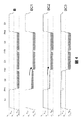
− フェーズΦ3はゼロに減らされ、
− フェーズΦ2はVddに上げられ、
− フェーズΦ4は0に減らされ、
− 最後にフェーズΦ1は、ラインAの構成に従い、0に減らされる。
− 図のラインA;Φ1、Φ4は0、Φ2、Φ3はVdd、
− 図のラインB;Φ4はVddに達し、
− 図のラインC;Φ2は0に達し、
− 図のラインD;Φ1はVddとなる。
− Φ2はVdd、Φ1およびΦ3は0、第2のゲートの下に電荷を保存する、
− Φ3はVddに達し、電荷はG2およびG3の下に拡散する、
− Φ2はゼロに達し、電荷はG3の下に集められる。これらはゲートG2からゲートG3まで前進したものである。
− Φ1はVddに達し、電荷はG3と次のピクセルのゲートG1との間で拡散する、
− Φ3はゼロに達し、電荷は次のピクセルのゲートG1の下で集められる。
以下同様に、フェーズの周期的循環を通じて、電荷は2ステップで1個のゲートから、および6ステップで完全な1個のピクセルから前進する。
12 エピタキシャル半導体層
14 領域
16 表面領域
A〜D ライン
BC1〜BC3 ライン
N ラインの個数
P ピクセル
G1〜G41 ゲート
PH1〜PH4 間隙
Φ1〜Φ4 制御フェーズ
VL,VH,Vdd 電位
Vbi、VbiH、VbiL 内蔵電位
Claims (5)
- 時間遅延および電荷積分を伴い動作する電荷移動画像センサであって、前記センサがP個のピクセルのN個の隣接ラインを、前記各種ライン内で所与のランクのピクセル内の画像点により生成された電荷が蓄積されたピクセルの複数のラインにより、全く同一の画像ラインを連続的に観察する目的で含み、前記ピクセルが、光透過性の絶縁ゲートに覆われた第1の種類の導電性を有する半導体層内に形成されていて、前記ゲートに高および低電位を交互に印加して、電荷の保存、次いで、1個のゲートから次のゲートへの指向的移動を可能にする手段が提供され、1個のピクセルが前記半導体層の上方に一連の複数の絶縁ゲートを含んでいて、1個のピクセルの前記ゲートは互いに分離されていて、且つ前記第1の種類のドープ表面領域に覆われた第2の種類の導電性を有するドープ領域上方に配置された、狭くて覆われていない間隙により、別のラインの隣接ピクセルのゲートから分離されていて、前記表面領域が全く同一の基準電位に保たれており、隣接するゲート間の前記狭い間隙の幅が、前記間隙に隣接するゲートが高および低電位を交互に受信した際に、前記第2の種類のドープ領域の内部電位が、前記狭い間隙の幅全体にわたり変更されることを特徴とする画像センサ。
- 前記基準電位が、前記第1の種類の半導体層の共通電位であることを特徴とする、請求項1に記載の画像センサ。
- 前記第1の種類の導電性を有する前記表面領域が全て、前記半導体層を接合する同一種類の深い拡散部と隣接していることを特徴とする、請求項2に記載の画像センサ。
- 前記ピクセルが、狭い間隙により分離された4個の隣接するゲートを含むこと、且つ4個のフェーズにより制御されること、すなわち前記各種ピクセルの同一行の全てのゲートが、前記4個のフェーズから取られた全く同一のフェーズを受信すること、を特徴とする、請求項1〜3のいずれか1項に記載の画像センサ。
- 前記ピクセルが、狭い間隙により分離された3個の隣接するゲートを含むこと、且つ3個のフェーズにより制御されること、すなわち前記各種のピクセルの全く同一の行の全てのゲートが、前記3個のフェーズから取られた全く同一のフェーズを受信すること、を特徴とする、請求項1〜3のいずれか1項に記載の画像センサ。
Applications Claiming Priority (2)
| Application Number | Priority Date | Filing Date | Title |
|---|---|---|---|
| FR1150658 | 2011-01-28 | ||
| FR1150658A FR2971084B1 (fr) | 2011-01-28 | 2011-01-28 | Capteur d'image multilineaire a integration de charges |
Publications (2)
| Publication Number | Publication Date |
|---|---|
| JP2012160731A true JP2012160731A (ja) | 2012-08-23 |
| JP5998409B2 JP5998409B2 (ja) | 2016-09-28 |
Family
ID=44454742
Family Applications (1)
| Application Number | Title | Priority Date | Filing Date |
|---|---|---|---|
| JP2012015418A Expired - Fee Related JP5998409B2 (ja) | 2011-01-28 | 2012-01-27 | 電荷積分多重線形画像センサ |
Country Status (7)
| Country | Link |
|---|---|
| US (1) | US8933495B2 (ja) |
| EP (1) | EP2482317B1 (ja) |
| JP (1) | JP5998409B2 (ja) |
| KR (1) | KR101968340B1 (ja) |
| CN (1) | CN102623479B (ja) |
| FR (1) | FR2971084B1 (ja) |
| IL (1) | IL217742A (ja) |
Cited By (1)
| Publication number | Priority date | Publication date | Assignee | Title |
|---|---|---|---|---|
| CN103986888A (zh) * | 2014-05-20 | 2014-08-13 | 天津大学 | 针对单粒子效应加固的tdi型cmos图像传感器累加电路 |
Families Citing this family (7)
| Publication number | Priority date | Publication date | Assignee | Title |
|---|---|---|---|---|
| FR2953642B1 (fr) * | 2009-12-09 | 2012-07-13 | E2V Semiconductors | Capteur d'image multilineaire a integration de charges. |
| US9049353B2 (en) | 2011-09-28 | 2015-06-02 | Semiconductor Components Industries, Llc | Time-delay-and-integrate image sensors having variable integration times |
| CN103094299B (zh) * | 2013-01-22 | 2015-06-17 | 南京理工大学 | 具有亚微米级间隙的高效电荷转移寄存器及其制备工艺 |
| FR3036848B1 (fr) | 2015-05-28 | 2017-05-19 | E2V Semiconductors | Capteur d'image a transfert de charges a double implantation de grille |
| FR3047112B1 (fr) | 2016-01-22 | 2018-01-19 | Teledyne E2V Semiconductors Sas | Capteur d'image multilineaire a transfert de charges a reglage de temps d'integration |
| US10469782B2 (en) * | 2016-09-27 | 2019-11-05 | Kla-Tencor Corporation | Power-conserving clocking for scanning sensors |
| CN117038684B (zh) * | 2023-07-14 | 2024-12-24 | 北京空间机电研究所 | 一种可精细调整电荷累加级数的tdi-cmos图像探测器 |
Citations (5)
| Publication number | Priority date | Publication date | Assignee | Title |
|---|---|---|---|---|
| JPS52155070A (en) * | 1976-06-18 | 1977-12-23 | Matsushita Electric Ind Co Ltd | Production of ccd |
| JPS60213061A (ja) * | 1984-04-09 | 1985-10-25 | Nec Corp | 電荷転送デバイス |
| JPH02229439A (ja) * | 1989-03-01 | 1990-09-12 | Matsushita Electron Corp | 電荷転送装置およびその駆動方法 |
| JPH10223877A (ja) * | 1997-02-07 | 1998-08-21 | Nec Corp | 固体撮像素子とその製造方法 |
| JP2005135965A (ja) * | 2003-10-28 | 2005-05-26 | Fuji Photo Film Co Ltd | 固体撮像素子およびその製造方法 |
Family Cites Families (10)
| Publication number | Priority date | Publication date | Assignee | Title |
|---|---|---|---|---|
| US6906749B1 (en) | 1998-09-16 | 2005-06-14 | Dalsa, Inc. | CMOS TDI image sensor |
| US6465820B1 (en) * | 1998-09-16 | 2002-10-15 | Dalsa, Inc. | CMOS compatible single phase CCD charge transfer device |
| WO2001026382A1 (en) | 1999-10-05 | 2001-04-12 | California Institute Of Technology | Time-delayed-integration imaging with active pixel sensors |
| US6680222B2 (en) * | 1999-11-05 | 2004-01-20 | Isetex, Inc | Split-gate virtual-phase CCD image sensor with a diffused lateral overflow anti-blooming drain structure and process of making |
| JP2005101486A (ja) * | 2003-08-28 | 2005-04-14 | Sanyo Electric Co Ltd | 固体撮像素子及びその制御方法 |
| US8446508B2 (en) * | 2005-07-27 | 2013-05-21 | Sony Corporation | Solid state imaging device with optimized locations of internal electrical components |
| FR2906080B1 (fr) | 2006-09-19 | 2008-11-28 | E2V Semiconductors Soc Par Act | Capteur d'image en defilement par integrations successives et sommation, a pixels cmos actifs |
| FR2906081B1 (fr) | 2006-09-19 | 2008-11-28 | E2V Semiconductors Soc Par Act | Capteur d'image lineaire cmos a fonctionnement de type transfert de charges |
| US7923763B2 (en) * | 2007-03-08 | 2011-04-12 | Teledyne Licensing, Llc | Two-dimensional time delay integration visible CMOS image sensor |
| JP4968227B2 (ja) * | 2008-10-03 | 2012-07-04 | 三菱電機株式会社 | イメージセンサ及びその駆動方法 |
-
2011
- 2011-01-28 FR FR1150658A patent/FR2971084B1/fr not_active Expired - Fee Related
-
2012
- 2012-01-18 EP EP12151572.0A patent/EP2482317B1/fr not_active Not-in-force
- 2012-01-20 CN CN201210056894.7A patent/CN102623479B/zh not_active Expired - Fee Related
- 2012-01-26 IL IL217742A patent/IL217742A/en active IP Right Grant
- 2012-01-26 US US13/359,200 patent/US8933495B2/en not_active Expired - Fee Related
- 2012-01-27 KR KR1020120008626A patent/KR101968340B1/ko not_active Expired - Fee Related
- 2012-01-27 JP JP2012015418A patent/JP5998409B2/ja not_active Expired - Fee Related
Patent Citations (5)
| Publication number | Priority date | Publication date | Assignee | Title |
|---|---|---|---|---|
| JPS52155070A (en) * | 1976-06-18 | 1977-12-23 | Matsushita Electric Ind Co Ltd | Production of ccd |
| JPS60213061A (ja) * | 1984-04-09 | 1985-10-25 | Nec Corp | 電荷転送デバイス |
| JPH02229439A (ja) * | 1989-03-01 | 1990-09-12 | Matsushita Electron Corp | 電荷転送装置およびその駆動方法 |
| JPH10223877A (ja) * | 1997-02-07 | 1998-08-21 | Nec Corp | 固体撮像素子とその製造方法 |
| JP2005135965A (ja) * | 2003-10-28 | 2005-05-26 | Fuji Photo Film Co Ltd | 固体撮像素子およびその製造方法 |
Cited By (1)
| Publication number | Priority date | Publication date | Assignee | Title |
|---|---|---|---|---|
| CN103986888A (zh) * | 2014-05-20 | 2014-08-13 | 天津大学 | 针对单粒子效应加固的tdi型cmos图像传感器累加电路 |
Also Published As
| Publication number | Publication date |
|---|---|
| KR20120087855A (ko) | 2012-08-07 |
| EP2482317A1 (fr) | 2012-08-01 |
| CN102623479B (zh) | 2016-01-13 |
| CN102623479A (zh) | 2012-08-01 |
| FR2971084B1 (fr) | 2013-08-23 |
| FR2971084A1 (fr) | 2012-08-03 |
| US8933495B2 (en) | 2015-01-13 |
| US20120193683A1 (en) | 2012-08-02 |
| IL217742A (en) | 2016-05-31 |
| JP5998409B2 (ja) | 2016-09-28 |
| IL217742A0 (en) | 2012-06-28 |
| KR101968340B1 (ko) | 2019-04-11 |
| EP2482317B1 (fr) | 2014-12-03 |
Similar Documents
| Publication | Publication Date | Title |
|---|---|---|
| JP5998409B2 (ja) | 電荷積分多重線形画像センサ | |
| CN108336101B (zh) | 飞行时间探测像素 | |
| CN102971852B (zh) | 具有非对称栅极的矩阵电荷转移图像传感器 | |
| JP6210559B2 (ja) | 半導体素子及び固体撮像装置 | |
| EP2453477B1 (en) | Solid state imaging element | |
| TWI521689B (zh) | 利用電荷積分的多重線性影像感測器 | |
| TW201633518A (zh) | 光感測器及其之訊號讀出方法以及固體攝像裝置及其之訊號讀出方法 | |
| JPH04505543A (ja) | インターライン転送ccdイメージセンサ装置におけるインターレース/非インターレースモードの選択作用 | |
| US20130075791A1 (en) | Depleted charge-multiplying ccd image sensor | |
| JP4777798B2 (ja) | 固体撮像装置とその駆動方法 | |
| JP6133973B2 (ja) | 非対称ゲートを備えた双方向電荷転送を実現するマトリクス画像センサ | |
| CN100502025C (zh) | 图像传感器 | |
| TWI711167B (zh) | 具有雙閘極植入之電荷轉移影像感測器 | |
| JPH03246971A (ja) | 電荷結合素子およびこれを用いた固体撮像装置 | |
| JPS5850874A (ja) | 固体撮像装置およびその駆動法 | |
| Fife et al. | Design and characterization of submicron ccds in cmos |
Legal Events
| Date | Code | Title | Description |
|---|---|---|---|
| A621 | Written request for application examination |
Free format text: JAPANESE INTERMEDIATE CODE: A621 Effective date: 20141218 |
|
| A521 | Request for written amendment filed |
Free format text: JAPANESE INTERMEDIATE CODE: A523 Effective date: 20150219 |
|
| A977 | Report on retrieval |
Free format text: JAPANESE INTERMEDIATE CODE: A971007 Effective date: 20150831 |
|
| A131 | Notification of reasons for refusal |
Free format text: JAPANESE INTERMEDIATE CODE: A131 Effective date: 20150908 |
|
| A521 | Request for written amendment filed |
Free format text: JAPANESE INTERMEDIATE CODE: A523 Effective date: 20151125 |
|
| TRDD | Decision of grant or rejection written | ||
| A01 | Written decision to grant a patent or to grant a registration (utility model) |
Free format text: JAPANESE INTERMEDIATE CODE: A01 Effective date: 20160614 |
|
| A61 | First payment of annual fees (during grant procedure) |
Free format text: JAPANESE INTERMEDIATE CODE: A61 Effective date: 20160701 |
|
| A61 | First payment of annual fees (during grant procedure) |
Free format text: JAPANESE INTERMEDIATE CODE: A61 Effective date: 20160812 |
|
| R150 | Certificate of patent or registration of utility model |
Ref document number: 5998409 Country of ref document: JP Free format text: JAPANESE INTERMEDIATE CODE: R150 |
|
| S533 | Written request for registration of change of name |
Free format text: JAPANESE INTERMEDIATE CODE: R313533 |
|
| R350 | Written notification of registration of transfer |
Free format text: JAPANESE INTERMEDIATE CODE: R350 |
|
| R250 | Receipt of annual fees |
Free format text: JAPANESE INTERMEDIATE CODE: R250 |
|
| R250 | Receipt of annual fees |
Free format text: JAPANESE INTERMEDIATE CODE: R250 |
|
| LAPS | Cancellation because of no payment of annual fees |