JP2012175103A - 光学装置、スキャン方法、リソグラフィ装置及びデバイス製造方法 - Google Patents
光学装置、スキャン方法、リソグラフィ装置及びデバイス製造方法 Download PDFInfo
- Publication number
- JP2012175103A JP2012175103A JP2012027606A JP2012027606A JP2012175103A JP 2012175103 A JP2012175103 A JP 2012175103A JP 2012027606 A JP2012027606 A JP 2012027606A JP 2012027606 A JP2012027606 A JP 2012027606A JP 2012175103 A JP2012175103 A JP 2012175103A
- Authority
- JP
- Japan
- Prior art keywords
- radiation
- substrate
- mirror
- mark
- objective lens
- Prior art date
- Legal status (The legal status is an assumption and is not a legal conclusion. Google has not performed a legal analysis and makes no representation as to the accuracy of the status listed.)
- Granted
Links
Images


Classifications
-
- H—ELECTRICITY
- H10—SEMICONDUCTOR DEVICES; ELECTRIC SOLID-STATE DEVICES NOT OTHERWISE PROVIDED FOR
- H10P—GENERIC PROCESSES OR APPARATUS FOR THE MANUFACTURE OR TREATMENT OF DEVICES COVERED BY CLASS H10
- H10P76/00—Manufacture or treatment of masks on semiconductor bodies, e.g. by lithography or photolithography
- H10P76/20—Manufacture or treatment of masks on semiconductor bodies, e.g. by lithography or photolithography of masks comprising organic materials
- H10P76/204—Manufacture or treatment of masks on semiconductor bodies, e.g. by lithography or photolithography of masks comprising organic materials of organic photoresist masks
-
- G—PHYSICS
- G02—OPTICS
- G02B—OPTICAL ELEMENTS, SYSTEMS OR APPARATUS
- G02B21/00—Microscopes
- G02B21/0004—Microscopes specially adapted for specific applications
- G02B21/002—Scanning microscopes
- G02B21/0024—Confocal scanning microscopes (CSOMs) or confocal "macroscopes"; Accessories which are not restricted to use with CSOMs, e.g. sample holders
- G02B21/0036—Scanning details, e.g. scanning stages
- G02B21/0048—Scanning details, e.g. scanning stages scanning mirrors, e.g. rotating or galvanomirrors, MEMS mirrors
-
- G—PHYSICS
- G01—MEASURING; TESTING
- G01B—MEASURING LENGTH, THICKNESS OR SIMILAR LINEAR DIMENSIONS; MEASURING ANGLES; MEASURING AREAS; MEASURING IRREGULARITIES OF SURFACES OR CONTOURS
- G01B11/00—Measuring arrangements characterised by the use of optical techniques
-
- G—PHYSICS
- G01—MEASURING; TESTING
- G01B—MEASURING LENGTH, THICKNESS OR SIMILAR LINEAR DIMENSIONS; MEASURING ANGLES; MEASURING AREAS; MEASURING IRREGULARITIES OF SURFACES OR CONTOURS
- G01B11/00—Measuring arrangements characterised by the use of optical techniques
- G01B11/14—Measuring arrangements characterised by the use of optical techniques for measuring distance or clearance between spaced objects or spaced apertures
-
- G—PHYSICS
- G02—OPTICS
- G02B—OPTICAL ELEMENTS, SYSTEMS OR APPARATUS
- G02B26/00—Optical devices or arrangements for the control of light using movable or deformable optical elements
- G02B26/08—Optical devices or arrangements for the control of light using movable or deformable optical elements for controlling the direction of light
- G02B26/10—Scanning systems
- G02B26/105—Scanning systems with one or more pivoting mirrors or galvano-mirrors
-
- G—PHYSICS
- G03—PHOTOGRAPHY; CINEMATOGRAPHY; ANALOGOUS TECHNIQUES USING WAVES OTHER THAN OPTICAL WAVES; ELECTROGRAPHY; HOLOGRAPHY
- G03F—PHOTOMECHANICAL PRODUCTION OF TEXTURED OR PATTERNED SURFACES, e.g. FOR PRINTING, FOR PROCESSING OF SEMICONDUCTOR DEVICES; MATERIALS THEREFOR; ORIGINALS THEREFOR; APPARATUS SPECIALLY ADAPTED THEREFOR
- G03F7/00—Photomechanical, e.g. photolithographic, production of textured or patterned surfaces, e.g. printing surfaces; Materials therefor, e.g. comprising photoresists; Apparatus specially adapted therefor
- G03F7/70—Microphotolithographic exposure; Apparatus therefor
- G03F7/70483—Information management; Active and passive control; Testing; Wafer monitoring, e.g. pattern monitoring
- G03F7/70605—Workpiece metrology
- G03F7/70616—Monitoring the printed patterns
- G03F7/70625—Dimensions, e.g. line width, critical dimension [CD], profile, sidewall angle or edge roughness
-
- G—PHYSICS
- G03—PHOTOGRAPHY; CINEMATOGRAPHY; ANALOGOUS TECHNIQUES USING WAVES OTHER THAN OPTICAL WAVES; ELECTROGRAPHY; HOLOGRAPHY
- G03F—PHOTOMECHANICAL PRODUCTION OF TEXTURED OR PATTERNED SURFACES, e.g. FOR PRINTING, FOR PROCESSING OF SEMICONDUCTOR DEVICES; MATERIALS THEREFOR; ORIGINALS THEREFOR; APPARATUS SPECIALLY ADAPTED THEREFOR
- G03F9/00—Registration or positioning of originals, masks, frames, photographic sheets or textured or patterned surfaces, e.g. automatically
- G03F9/70—Registration or positioning of originals, masks, frames, photographic sheets or textured or patterned surfaces, e.g. automatically for microlithography
- G03F9/7088—Alignment mark detection, e.g. TTR, TTL, off-axis detection, array detector, video detection
-
- H—ELECTRICITY
- H10—SEMICONDUCTOR DEVICES; ELECTRIC SOLID-STATE DEVICES NOT OTHERWISE PROVIDED FOR
- H10P—GENERIC PROCESSES OR APPARATUS FOR THE MANUFACTURE OR TREATMENT OF DEVICES COVERED BY CLASS H10
- H10P76/00—Manufacture or treatment of masks on semiconductor bodies, e.g. by lithography or photolithography
- H10P76/20—Manufacture or treatment of masks on semiconductor bodies, e.g. by lithography or photolithography of masks comprising organic materials
- H10P76/204—Manufacture or treatment of masks on semiconductor bodies, e.g. by lithography or photolithography of masks comprising organic materials of organic photoresist masks
- H10P76/2041—Photolithographic processes
Landscapes
- Physics & Mathematics (AREA)
- General Physics & Mathematics (AREA)
- Optics & Photonics (AREA)
- Engineering & Computer Science (AREA)
- Multimedia (AREA)
- Chemical & Material Sciences (AREA)
- Analytical Chemistry (AREA)
- Exposure And Positioning Against Photoresist Photosensitive Materials (AREA)
- Length Measuring Devices By Optical Means (AREA)
- Exposure Of Semiconductors, Excluding Electron Or Ion Beam Exposure (AREA)
Abstract
【解決手段】装置は、リソグラフィ基板W上のマーク202の位置を測定する。測定光学システムは、マークを放射スポットで照明する照明サブシステムと、マークによって回折した放射を検出する検出サブシステム580とを備える。傾斜ミラー562は、放射スポットを、マーク自体のスキャン運動と同期して測定光学システムの基準フレームに対して移動させて、正確な位置測定値を取得するより多くの時間を提供する。ミラー傾斜軸568は、ミラー平面と対物レンズ524の瞳面Pとの交点に沿って配置され、スキャンのアーティファクトを最小限にする。他のタイプの装置、例えば共焦顕微鏡におけるスキャンのために同じ幾何学的構成を使用できる。
【選択図】図5
Description
− 放射ビームB(例えばUV放射又はEUV放射)を調節するように構成された照明システム(イルミネータ)ILと、
− パターニングデバイス(例えばマスク)MAを支持するように構築され、特定のパラメータに従ってパターニングデバイスを正確に位置決めするように構成された第1のポジショナPMに接続された支持構造(例えばマスクテーブル)MTと、
− 基板(例えばレジストコートウェーハ)Wを保持するように構築され、特定のパラメータに従って基板を正確に位置決めするように構成された第2のポジショナPWに接続された基板テーブル(例えばウェーハテーブル)WTと、
− パターニングデバイスMAによって放射ビームBに与えられたパターンを基板Wのターゲット部分C(例えば1つ又は複数のダイを含む)に投影するように構成された投影システム(例えば屈折投影レンズシステム)PSとを備える。
1.ステップモードにおいては、マスクテーブルMT及び基板テーブルWTa/WTbは、基本的に静止状態に維持される一方、放射ビームに与えたパターン全体が1回でターゲット部分Cに投影される(すなわち単一静的露光)。次に、別のターゲット部分Cを露光できるように、基板テーブルWTa/WTbがX方向及び/又はY方向に移動される。ステップモードでは、露光フィールドの最大サイズによって、単一静的露光で像が形成されるターゲット部分Cのサイズが制限される。
2.スキャンモードにおいては、マスクテーブルMT及び基板テーブルWTa/WTbは同期的にスキャンされる一方、放射ビームに与えられるパターンがターゲット部分Cに投影される(すなわち単一動的露光)。マスクテーブルMTに対する基板テーブルWTa/WTbの速度及び方向は、投影システムPSの拡大(縮小)及び像反転特性によって求めることができる。スキャンモードでは、露光フィールドの最大サイズによって、単一動的露光におけるターゲット部分の(非スキャン方向における)幅が制限され、スキャン動作の長さによってターゲット部分の(スキャン方向における)高さが決まる。
3.別のモードでは、マスクテーブルMTはプログラマブルパターニングデバイスを保持して基本的に静止状態に維持され、基板テーブルWTa/WTbを移動又はスキャンさせながら、放射ビームに与えられたパターンをターゲット部分Cに投影する。このモードでは、一般にパルス状放射源を使用して、基板テーブルWTa/WTbを移動させる毎に、又はスキャン中に連続する放射パルスの間で、プログラマブルパターニングデバイスを必要に応じて更新する。この動作モードは、以上で言及したようなタイプのプログラマブルミラーアレイなどのプログラマブルパターニングデバイスを使用するマスクレスリソグラフィに容易に利用できる。
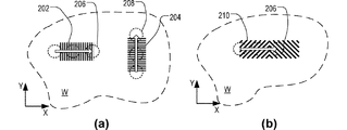
[0051] 例示的実施形態の検出器530a及び530bはその領域にわたってピクセルを有する画像センサとして記述されているが、検出器が瞳像平面P”の一定の地点にだけ提供される代替実施形態も可能である。特に、1次回折照明が予想される周辺位置に数個の検出器を配置することでアライメント信号を入手できる。瞳像の周辺全体に一組の検出器を離間させることができ、マーク202がX方向かY方向か、又は図2(b)に示すタイプのX−Yマークかに従って、位置測定値を生成する処理を実行するために適当な検出器からの信号を選択することができる。
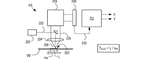
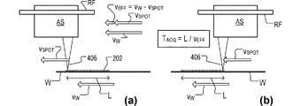
[0057] アライメントセンサは、ミラーとミラーが使用される光学システムの瞳面と同じ平面に位置するように枢動軸が変位される傾斜ミラーの用途例である。この構成は、基板上への平均入射角を変更することなく照明スポットを基板平面内で偏向させる特殊な能力を有する。アライメントセンサ以外の用途にこの原理を適用でき、共焦顕微鏡は別の例である。
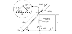
[0061] 上記の例では、揺動ミラーは約90°の角度で光学経路を方向転換させ、対物レンズ524又は1524の瞳面に対して45°の角度に装着される。ミラー平面と対物レンズ524/1524の瞳面Pとの交点にミラー562/1562の枢動軸を配置するという同じ原理を45°以外の角度に拡張することができる。

Claims (15)
- 該装置の光学システムとオブジェクトとの間で放射線を伝送する対物レンズを備える光学装置であって、
前記光学システムと前記対物レンズとの間に配置され、前記対物レンズを前記放射線が通過する際に前記放射線の方向を変えるように傾斜するミラーを備える、少なくとも1つの可動素子をさらに備え、
前記ミラーが、前記対物レンズの瞳面と前記ミラーの平面との間の交点にほぼ沿った軸を中心に傾斜するように強制される、光学装置。 - 前記可動素子は、揺動して前記放射線に繰り返しスキャン運動を付与するように装着される、請求項1に記載の装置。
- 前記可動光学素子は、共振周波数で揺動するように装着される、請求項2に記載の装置。
- 基板上のマークの位置を測定する請求項1乃至3のいずれかに記載の装置であって、
前記マークを前記対物レンズを介して放射スポットで照明する照明サブシステムと、前記マークによって回折した放射を前記対物レンズを介して検出する検出サブシステムとを備える前記光学システムと、
前記基板と測定光学システムの動きを互いに対して第1の速度で制御して、前記マークを前記放射スポットでスキャンしながら、前記回折放射を表す信号を検出し処理して前記測定光学システムの基準フレームに対する前記マークの位置を計算する第1の位置決めサブシステムと、
前記放射スポットを前記測定光学システムの前記基準フレームに対して第2の速度で移動させるために前記第1の位置決めサブシステムと同期して動作可能な前記可動光学素子とを備え、
前記第1及び第2の速度が、前記信号が検出されている間に前記第1の速度より低い第3の速度で前記スポットが前記マークをスキャンする関係にある、装置。 - 動作時に前記第1及び第2の速度が並列であり、前記第2の速度が前記第1の速度より低く、前記第3の速度が前記第1の速度から前記第2の速度を引いたものに等しい、請求項4に記載の装置。
- 前記対物レンズは、前記測定光学システムの前記基準フレームとの関係で固定されている、請求項4又は5に記載の装置。
- 前記光学システムは、前記回折放射の2つの部分を回転させ再結合する自己参照型干渉計を含む、請求項4、5又は6に記載の装置。
- オブジェクトの検査のための共焦顕微鏡を備える、請求項1、2又は3に記載の装置であって、
オブジェクトを前記対物レンズを介して放射スポットで照明する照明サブシステムと、前記オブジェクトによって前記放射スポットにおける特定の地点で反射された放射を前記対物レンズを介して検出する検出サブシステムとを備える前記光学システムと、
前記放射スポットと前記特定の地点とを少なくとも第1のスキャン方向にスキャンして、前記オブジェクトにわたって地点の線から検出された放射強度を記録するように動作可能な前記可動光学素子と
を備える装置。 - 前記オブジェクトと前記対物レンズとを互いに対して第2のスキャン方向に移動させて、前記オブジェクトにわたって一連の地点の線からの放射強度を記録する位置決めサブシステムをさらに備える、請求項8に記載の装置。
- パターニングデバイスから基板上にパターンを転写するように構成されたリソグラフィ装置であって、
基板を保持する基板テーブルと、前記リソグラフィ装置の基準フレームに対する前記基板上のマークの位置を測定するアライメントセンサとを備え、
前記アライメントセンサが、請求項4から7のいずれかに記載の測定装置を備え、
前記リソグラフィ装置が、前記測定装置を用いて測定される前記基板上のマークの位置を基準にして前記基板上へのパターンの転写を制御するように構成された、リソグラフィ装置。 - オブジェクトを対物レンズを介して放射線でスキャンする方法であって、
前記対物レンズの前に前記放射線の経路内にミラーを配置すること、及び
前記放射線が対物レンズを通過する際に前記放射線の方向を変更するようにミラーを傾斜させて、それにより前記ミラーの傾斜角に従って前記放射線を前記オブジェクトの異なる部分に入射させることを含み、
前記ミラーが、前記対物レンズの瞳面と前記ミラーの平面との間の交点にほぼ沿った軸を中心に傾斜するように強制される、方法。 - 前記ミラーは、揺動して前記放射線に繰り返しスキャン運動を付与するように装着される、請求項11に記載の方法。
- 前記可動光学素子は、共振周波数で揺動するように装着され駆動される、請求項12に記載の方法。
- 前記スキャンが、基板上のマークの位置を測定する工程の一部として実行される、請求項11、12又は13に記載の方法。
- リソグラフィ工程が、パターニングデバイスから基板上にパターンを転写するために使用され、前記基板上へのパターンの転写が、請求項14に記載の方法を用いて測定される前記基板上のマークの位置を基準にして制御される、デバイス製造方法。
Applications Claiming Priority (4)
| Application Number | Priority Date | Filing Date | Title |
|---|---|---|---|
| US201161444373P | 2011-02-18 | 2011-02-18 | |
| US61/444,373 | 2011-02-18 | ||
| US201161468208P | 2011-03-28 | 2011-03-28 | |
| US61/468,208 | 2011-03-28 |
Publications (2)
| Publication Number | Publication Date |
|---|---|
| JP2012175103A true JP2012175103A (ja) | 2012-09-10 |
| JP5466721B2 JP5466721B2 (ja) | 2014-04-09 |
Family
ID=46652455
Family Applications (2)
| Application Number | Title | Priority Date | Filing Date |
|---|---|---|---|
| JP2012027626A Active JP5438148B2 (ja) | 2011-02-18 | 2012-02-10 | 測定方法、測定装置、及びリソグラフィ装置 |
| JP2012027606A Active JP5466721B2 (ja) | 2011-02-18 | 2012-02-10 | 光学装置、スキャン方法、リソグラフィ装置及びデバイス製造方法 |
Family Applications Before (1)
| Application Number | Title | Priority Date | Filing Date |
|---|---|---|---|
| JP2012027626A Active JP5438148B2 (ja) | 2011-02-18 | 2012-02-10 | 測定方法、測定装置、及びリソグラフィ装置 |
Country Status (6)
| Country | Link |
|---|---|
| US (2) | US9303978B2 (ja) |
| JP (2) | JP5438148B2 (ja) |
| KR (2) | KR101365146B1 (ja) |
| CN (2) | CN102645847A (ja) |
| NL (2) | NL2008111A (ja) |
| TW (2) | TWI459153B (ja) |
Cited By (8)
| Publication number | Priority date | Publication date | Assignee | Title |
|---|---|---|---|---|
| JP2012191177A (ja) * | 2011-02-18 | 2012-10-04 | Asml Netherlands Bv | 測定方法、測定装置、リソグラフィ装置及びデバイス製造方法 |
| WO2015098282A1 (ja) * | 2013-12-26 | 2015-07-02 | 東京エレクトロン株式会社 | 基板処理システム、基板搬送方法及びコンピュータ記憶媒体 |
| WO2016104511A1 (ja) * | 2014-12-24 | 2016-06-30 | 株式会社ニコン | 計測装置及び計測方法、露光装置及び露光方法、並びにデバイス製造方法 |
| WO2016125790A1 (ja) * | 2015-02-05 | 2016-08-11 | 株式会社ニコン | 計測装置及び計測方法、露光装置及び露光方法、並びにデバイス製造方法 |
| JPWO2016104513A1 (ja) * | 2014-12-24 | 2017-11-24 | 株式会社ニコン | 移動体の制御方法、露光方法、デバイス製造方法、移動体装置、及び露光装置 |
| JP2018527630A (ja) * | 2015-08-28 | 2018-09-20 | エーエスエムエル ネザーランズ ビー.ブイ. | リソグラフィ装置、リソグラフィアライメント方法およびデータ処理システム |
| JP2019504364A (ja) * | 2016-01-26 | 2019-02-14 | シャンハイ マイクロ エレクトロニクス イクイプメント(グループ)カンパニー リミティド | スキャン反射性ミラー監視システム及び方法、フォーカス・レベリングシステム |
| JP2021535419A (ja) * | 2018-08-29 | 2021-12-16 | エーエスエムエル ホールディング エヌ.ブイ. | コンパクトなアライメントセンサ配置 |
Families Citing this family (48)
| Publication number | Priority date | Publication date | Assignee | Title |
|---|---|---|---|---|
| EP2458441B1 (en) * | 2010-11-30 | 2022-01-19 | ASML Netherlands BV | Measuring method, apparatus and substrate |
| JP5873212B2 (ja) | 2012-04-12 | 2016-03-01 | エーエスエムエル ネザーランズ ビー.ブイ. | 位置測定方法、位置測定装置、リソグラフィ装置及びデバイス製造方法並びに光学要素 |
| NL2010717A (en) * | 2012-05-21 | 2013-11-25 | Asml Netherlands Bv | Determining a structural parameter and correcting an asymmetry property. |
| NL2011173A (en) | 2012-07-30 | 2014-02-03 | Asml Netherlands Bv | Position measuring apparatus, position measuring method, lithographic apparatus and device manufacturing method. |
| US9778025B2 (en) | 2012-08-16 | 2017-10-03 | Asml Netherlands B.V. | Method and apparatus for measuring asymmetry of a microstructure, position measuring method, position measuring apparatus, lithographic apparatus and device manufacturing method |
| NL2011477A (en) | 2012-10-10 | 2014-04-14 | Asml Netherlands Bv | Mark position measuring apparatus and method, lithographic apparatus and device manufacturing method. |
| WO2014062972A1 (en) * | 2012-10-18 | 2014-04-24 | Kla-Tencor Corporation | Symmetric target design in scatterometry overlay metrology |
| CN103777476B (zh) * | 2012-10-19 | 2016-01-27 | 上海微电子装备有限公司 | 一种离轴对准系统及对准方法 |
| NL2011681C2 (en) * | 2012-10-26 | 2014-05-01 | Mapper Lithography Ip Bv | Method of determining a position of a substrate in a lithography system, substrate for use in such method, and lithography system for carrying out such method. |
| WO2014068116A1 (en) * | 2012-11-05 | 2014-05-08 | Asml Netherlands B.V. | Method and apparatus for measuring asymmetry of a microstructure, position measuring method, position measuring apparatus, lithographic apparatus and device manufacturing method |
| US8941085B2 (en) | 2013-03-14 | 2015-01-27 | Taiwan Semiconductor Manufacturing Company, Ltd. | Electron beam lithography systems and methods including time division multiplex loading |
| US9030661B1 (en) * | 2013-03-15 | 2015-05-12 | Kla-Tencor Corporation | Alignment measurement system |
| JP6181284B2 (ja) | 2013-03-20 | 2017-08-16 | エーエスエムエル ネザーランズ ビー.ブイ. | 微小構造の非対称性の測定方法ならびに測定装置、位置測定方法、位置測定装置、リソグラフィ装置およびデバイス製造方法 |
| US9696264B2 (en) | 2013-04-03 | 2017-07-04 | Kla-Tencor Corporation | Apparatus and methods for determining defect depths in vertical stack memory |
| WO2014193854A1 (en) * | 2013-05-27 | 2014-12-04 | Kla-Tencor Corporation | Scatterometry overlay metrology targets and methods |
| US9740108B2 (en) * | 2013-05-27 | 2017-08-22 | Kla-Tencor Corporation | Scatterometry overlay metrology targets and methods |
| CN104375383B (zh) * | 2013-08-13 | 2017-08-29 | 上海微电子装备有限公司 | 用于光刻设备的调焦调平检测装置及方法 |
| NL2013457A (en) | 2013-10-09 | 2015-04-13 | Asml Netherlands Bv | Polarization independent interferometer. |
| CN105900016B (zh) * | 2013-12-05 | 2018-02-13 | Asml荷兰有限公司 | 用于测量衬底上的结构的方法和设备、用于误差校正的模型、用于实施这样的方法和设备的计算机程序产品 |
| JP6306724B2 (ja) * | 2014-01-09 | 2018-04-04 | ザイゴ コーポレーションZygo Corporation | 非球面およびその他の非平坦面のトポグラフィの測定 |
| JP6341883B2 (ja) * | 2014-06-27 | 2018-06-13 | キヤノン株式会社 | 位置検出装置、位置検出方法、インプリント装置及び物品の製造方法 |
| JP6496808B2 (ja) | 2014-08-25 | 2019-04-10 | エーエスエムエル ホールディング エヌ.ブイ. | 測定方法、測定装置、リソグラフィ装置、及びデバイス製造方法 |
| JP6470528B2 (ja) * | 2014-09-05 | 2019-02-13 | キヤノン株式会社 | 検出装置、計測装置、露光装置、物品の製造方法、および計測方法 |
| CN107430352B (zh) * | 2015-03-25 | 2020-01-21 | Asml荷兰有限公司 | 量测方法、量测设备和器件制造方法 |
| NL2016543A (en) * | 2015-04-16 | 2016-10-19 | Asml Holding Nv | Method and apparatus for optical fiber connection. |
| WO2017093256A1 (en) | 2015-12-03 | 2017-06-08 | Asml Netherlands B.V. | Position measuring method of an alignment target |
| US10607873B2 (en) | 2016-03-30 | 2020-03-31 | Asml Netherlands B.V. | Substrate edge detection |
| NL2018376A (en) | 2016-04-12 | 2017-10-17 | Asml Netherlands Bv | Mark Position Determination Method |
| IL263515B2 (en) | 2016-06-09 | 2023-03-01 | Asml Netherlands Bv | source of radiation |
| TWI800855B (zh) * | 2016-06-20 | 2023-05-01 | 日商尼康股份有限公司 | 具有失真匹配的密集線極紫外光微影系統以及將圖案轉移至工件上的方法 |
| TWI583982B (zh) | 2016-09-26 | 2017-05-21 | 峰安車業股份有限公司 | 位移量測裝置及加工系統 |
| DE102016012500A1 (de) * | 2016-10-19 | 2018-04-19 | Texmag Gmbh Vertriebsgesellschaft | Verfahren und Vorrichtung zur Lageerfassung einer laufenden Warenbahn |
| NL2020921A (en) | 2017-06-07 | 2018-12-13 | Stichting Vu | Alignment Measurement System |
| NL2021218A (en) | 2017-08-16 | 2019-02-25 | Asml Netherlands Bv | Alignment Measurement System |
| CN112005157B (zh) * | 2018-02-27 | 2023-03-03 | Asml荷兰有限公司 | 用于确定衬底上的一个或更多个结构的特性的量测设备和方法 |
| US11971665B2 (en) * | 2019-02-21 | 2024-04-30 | Asml Holding N.V. | Wafer alignment using form birefringence of targets or product |
| JP7430194B2 (ja) * | 2019-02-26 | 2024-02-09 | エーエスエムエル ネザーランズ ビー.ブイ. | 検査装置、リソグラフィ装置及び測定方法 |
| US11073768B2 (en) * | 2019-06-26 | 2021-07-27 | Kla Corporation | Metrology target for scanning metrology |
| US11994808B2 (en) | 2019-09-27 | 2024-05-28 | Asml Holding N.V. | Lithographic apparatus, metrology systems, phased array illumination sources and methods thereof |
| CN111508932B (zh) * | 2020-04-27 | 2021-12-14 | 深圳中科飞测科技股份有限公司 | 套刻标记及套刻误差的测量方法 |
| US12287583B2 (en) * | 2020-06-16 | 2025-04-29 | Asml Netherlands B.V. | Method for modeling measurement data over a substrate area and associated apparatuses |
| US11521874B2 (en) * | 2020-09-30 | 2022-12-06 | Kla Corporation | Systems and methods for determining measurement location in semiconductor wafer metrology |
| JP7614858B2 (ja) * | 2021-01-26 | 2025-01-16 | キヤノン株式会社 | 検出装置、リソグラフィ装置、および物品製造方法 |
| WO2022212738A1 (en) * | 2021-03-31 | 2022-10-06 | The Regents Of The University Of California | Uv lithography system and method |
| US20250028258A1 (en) * | 2021-08-20 | 2025-01-23 | Asml Netherlands B.V. | Compensating optical system for nonuniform surfaces, a metrology system, lithographic apparatus, and methods thereof |
| CN114046731B (zh) * | 2021-10-29 | 2023-03-14 | 西安工程大学 | 基于硅光电倍增管的亚微米单光子量级微小光斑测量方法 |
| JP2024098435A (ja) * | 2023-01-10 | 2024-07-23 | キオクシア株式会社 | 計測装置、及び、計測方法 |
| CN118068660B (zh) * | 2024-03-29 | 2025-05-27 | 上海微电子装备(集团)股份有限公司 | 曝光设备 |
Citations (8)
| Publication number | Priority date | Publication date | Assignee | Title |
|---|---|---|---|---|
| JPS6180215A (ja) * | 1984-09-28 | 1986-04-23 | Nippon Jido Seigyo Kk | 走査型顕微鏡撮像装置 |
| JPH02232918A (ja) * | 1989-03-07 | 1990-09-14 | Nikon Corp | 位置検出装置 |
| JPH06302499A (ja) * | 1993-04-09 | 1994-10-28 | Canon Inc | 位置検出装置及びそれを用いた半導体素子の製造方法 |
| JP2003247807A (ja) * | 2002-02-25 | 2003-09-05 | Hitachi Ltd | 合わせ精度計測装置及びその方法並びに半導体装置の製造方法及びそのシステム |
| JP2008263187A (ja) * | 2007-03-30 | 2008-10-30 | Asml Netherlands Bv | 角度分解スキャトロメータ、検査方法、リソグラフィ装置、リソグラフィ処理セル、デバイス製造方法およびアラインメントセンサ |
| JP2009047460A (ja) * | 2007-08-15 | 2009-03-05 | Lasertec Corp | 共焦点顕微鏡 |
| JP2009186555A (ja) * | 2008-02-04 | 2009-08-20 | Nsk Ltd | 露光装置 |
| JP2012191177A (ja) * | 2011-02-18 | 2012-10-04 | Asml Netherlands Bv | 測定方法、測定装置、リソグラフィ装置及びデバイス製造方法 |
Family Cites Families (17)
| Publication number | Priority date | Publication date | Assignee | Title |
|---|---|---|---|---|
| FR2523351B1 (fr) * | 1982-03-09 | 1989-07-13 | Thomson Csf | Tete optique dans un dispositif d'enregistrement-lecture d'un support d'information |
| JP2884947B2 (ja) * | 1992-10-01 | 1999-04-19 | 株式会社ニコン | 投影露光装置、露光方法および半導体集積回路の製造方法 |
| WO1998039689A1 (en) | 1997-03-07 | 1998-09-11 | Asm Lithography B.V. | Lithographic projection apparatus with off-axis alignment unit |
| DE60319462T2 (de) * | 2002-06-11 | 2009-03-12 | Asml Netherlands B.V. | Lithographischer Apparat und Verfahren zur Herstellung eines Artikels |
| TWI227814B (en) * | 2002-09-20 | 2005-02-11 | Asml Netherlands Bv | Alignment system and methods for lithographic systems using at least two wavelengths |
| US7341822B2 (en) | 2003-02-25 | 2008-03-11 | Asml Netherlands B.V. | Time-optimal setpoint generator in a lithographic apparatus |
| US7791727B2 (en) | 2004-08-16 | 2010-09-07 | Asml Netherlands B.V. | Method and apparatus for angular-resolved spectroscopic lithography characterization |
| US20060061743A1 (en) | 2004-09-22 | 2006-03-23 | Asml Netherlands B.V. | Lithographic apparatus, alignment system, and device manufacturing method |
| US7626701B2 (en) * | 2004-12-27 | 2009-12-01 | Asml Netherlands B.V. | Lithographic apparatus with multiple alignment arrangements and alignment measuring method |
| US7515281B2 (en) * | 2005-04-08 | 2009-04-07 | Asml Netherlands B.V. | Lithographic apparatus and device manufacturing method |
| US7626181B2 (en) | 2005-12-09 | 2009-12-01 | Asml Netherlands B.V. | Lithographic apparatus and device manufacturing method |
| DE102007009550B4 (de) | 2007-02-27 | 2008-12-18 | Ludwig-Maximilian-Universität | Verfahren und Mikroskopvorrichtung zur Beobachtung einer bewegten Probe |
| EP2048543B1 (en) * | 2007-10-09 | 2013-12-04 | ASML Netherlands B.V. | An optical focus sensor, an inspection apparatus and a lithographic apparatus |
| EP2048542A2 (en) * | 2007-10-09 | 2009-04-15 | ASML Netherlands B.V. | Alignment method and apparatus, lithographic apparatus, metrology apparatus and device manufacturing method |
| NL1036476A1 (nl) | 2008-02-01 | 2009-08-04 | Asml Netherlands Bv | Alignment mark and a method of aligning a substrate comprising such an alignment mark. |
| US8120781B2 (en) | 2008-11-26 | 2012-02-21 | Zygo Corporation | Interferometric systems and methods featuring spectral analysis of unevenly sampled data |
| NL2004094A (en) | 2009-02-11 | 2010-08-12 | Asml Netherlands Bv | Inspection apparatus, lithographic apparatus, lithographic processing cell and inspection method. |
-
2012
- 2012-01-12 NL NL2008111A patent/NL2008111A/en not_active Application Discontinuation
- 2012-01-12 NL NL2008110A patent/NL2008110A/en not_active Application Discontinuation
- 2012-01-17 US US13/351,728 patent/US9303978B2/en not_active Expired - Fee Related
- 2012-02-09 US US13/369,614 patent/US8593646B2/en not_active Expired - Fee Related
- 2012-02-10 JP JP2012027626A patent/JP5438148B2/ja active Active
- 2012-02-10 JP JP2012027606A patent/JP5466721B2/ja active Active
- 2012-02-13 TW TW101104570A patent/TWI459153B/zh not_active IP Right Cessation
- 2012-02-13 TW TW101104574A patent/TWI448844B/zh active
- 2012-02-14 CN CN2012100330017A patent/CN102645847A/zh active Pending
- 2012-02-14 CN CN201210033098.1A patent/CN102681167B/zh active Active
- 2012-02-17 KR KR1020120016248A patent/KR101365146B1/ko active Active
- 2012-02-17 KR KR1020120016249A patent/KR101386057B1/ko not_active Expired - Fee Related
Patent Citations (8)
| Publication number | Priority date | Publication date | Assignee | Title |
|---|---|---|---|---|
| JPS6180215A (ja) * | 1984-09-28 | 1986-04-23 | Nippon Jido Seigyo Kk | 走査型顕微鏡撮像装置 |
| JPH02232918A (ja) * | 1989-03-07 | 1990-09-14 | Nikon Corp | 位置検出装置 |
| JPH06302499A (ja) * | 1993-04-09 | 1994-10-28 | Canon Inc | 位置検出装置及びそれを用いた半導体素子の製造方法 |
| JP2003247807A (ja) * | 2002-02-25 | 2003-09-05 | Hitachi Ltd | 合わせ精度計測装置及びその方法並びに半導体装置の製造方法及びそのシステム |
| JP2008263187A (ja) * | 2007-03-30 | 2008-10-30 | Asml Netherlands Bv | 角度分解スキャトロメータ、検査方法、リソグラフィ装置、リソグラフィ処理セル、デバイス製造方法およびアラインメントセンサ |
| JP2009047460A (ja) * | 2007-08-15 | 2009-03-05 | Lasertec Corp | 共焦点顕微鏡 |
| JP2009186555A (ja) * | 2008-02-04 | 2009-08-20 | Nsk Ltd | 露光装置 |
| JP2012191177A (ja) * | 2011-02-18 | 2012-10-04 | Asml Netherlands Bv | 測定方法、測定装置、リソグラフィ装置及びデバイス製造方法 |
Cited By (26)
| Publication number | Priority date | Publication date | Assignee | Title |
|---|---|---|---|---|
| JP2012191177A (ja) * | 2011-02-18 | 2012-10-04 | Asml Netherlands Bv | 測定方法、測定装置、リソグラフィ装置及びデバイス製造方法 |
| US8593646B2 (en) | 2011-02-18 | 2013-11-26 | Asml Netherlands B.V. | Measuring method, measuring apparatus, lithographic apparatus and device manufacturing method |
| US9303978B2 (en) | 2011-02-18 | 2016-04-05 | Asml Netherlands B.V. | Optical apparatus, method of scanning, lithographic apparatus and device manufacturing method |
| WO2015098282A1 (ja) * | 2013-12-26 | 2015-07-02 | 東京エレクトロン株式会社 | 基板処理システム、基板搬送方法及びコンピュータ記憶媒体 |
| JP2015126083A (ja) * | 2013-12-26 | 2015-07-06 | 東京エレクトロン株式会社 | 基板処理システム、基板搬送方法、プログラム及びコンピュータ記憶媒体 |
| JPWO2016104513A1 (ja) * | 2014-12-24 | 2017-11-24 | 株式会社ニコン | 移動体の制御方法、露光方法、デバイス製造方法、移動体装置、及び露光装置 |
| US11994811B2 (en) | 2014-12-24 | 2024-05-28 | Nikon Corporation | Control method of movable body, exposure method, device manufacturing method, movable body apparatus, and exposure apparatus |
| JPWO2016104511A1 (ja) * | 2014-12-24 | 2017-09-28 | 株式会社ニコン | 計測装置及び計測方法、露光装置及び露光方法、並びにデバイス製造方法 |
| JP7147738B2 (ja) | 2014-12-24 | 2022-10-05 | 株式会社ニコン | 計測装置及び計測方法、並びに露光装置 |
| CN107407894A (zh) * | 2014-12-24 | 2017-11-28 | 株式会社尼康 | 测量装置及测量方法、曝光装置及曝光方法、以及器件制造方法 |
| JP2018139010A (ja) * | 2014-12-24 | 2018-09-06 | 株式会社ニコン | 移動体装置及び露光装置 |
| US12164236B2 (en) | 2014-12-24 | 2024-12-10 | Nikon Corporation | Measurement device and measurement method, exposure apparatus and exposure method, and device manufacturing method |
| WO2016104511A1 (ja) * | 2014-12-24 | 2016-06-30 | 株式会社ニコン | 計測装置及び計測方法、露光装置及び露光方法、並びにデバイス製造方法 |
| US10372046B2 (en) | 2014-12-24 | 2019-08-06 | Nikon Corporation | Measurement device and measurement method, exposure apparatus and exposure method, and device manufacturing method |
| US11567419B2 (en) | 2014-12-24 | 2023-01-31 | Nikon Corporation | Control method of movable body, exposure method, device manufacturing method, movable body apparatus, and exposure apparatus |
| CN107407894B (zh) * | 2014-12-24 | 2020-01-24 | 株式会社尼康 | 测量装置及测量方法、曝光装置及曝光方法、以及器件制造方法 |
| JP2020052430A (ja) * | 2014-12-24 | 2020-04-02 | 株式会社ニコン | 計測装置及び計測方法、並びに露光装置 |
| US10642169B2 (en) | 2014-12-24 | 2020-05-05 | Nikon Corporation | Measurement device and measurement method, exposure apparatus and exposure method, and device manufacturing method |
| US11003100B2 (en) | 2014-12-24 | 2021-05-11 | Nikon Corporation | Control method of movable body, exposure method, device manufacturing method, movable body apparatus, and exposure apparatus |
| WO2016125790A1 (ja) * | 2015-02-05 | 2016-08-11 | 株式会社ニコン | 計測装置及び計測方法、露光装置及び露光方法、並びにデバイス製造方法 |
| US10386735B2 (en) | 2015-08-28 | 2019-08-20 | Asml Netherlands B.V. | Lithographic apparatus alignment sensor and method |
| JP2018527630A (ja) * | 2015-08-28 | 2018-09-20 | エーエスエムエル ネザーランズ ビー.ブイ. | リソグラフィ装置、リソグラフィアライメント方法およびデータ処理システム |
| JP2019504364A (ja) * | 2016-01-26 | 2019-02-14 | シャンハイ マイクロ エレクトロニクス イクイプメント(グループ)カンパニー リミティド | スキャン反射性ミラー監視システム及び方法、フォーカス・レベリングシステム |
| JP7124205B2 (ja) | 2018-08-29 | 2022-08-23 | エーエスエムエル ホールディング エヌ.ブイ. | コンパクトなアライメントセンサ配置 |
| JP2021535419A (ja) * | 2018-08-29 | 2021-12-16 | エーエスエムエル ホールディング エヌ.ブイ. | コンパクトなアライメントセンサ配置 |
| US11531280B2 (en) | 2018-08-29 | 2022-12-20 | Asml Holding N.V. | Compact alignment sensor arrangements |
Also Published As
| Publication number | Publication date |
|---|---|
| CN102681167B (zh) | 2015-03-18 |
| TWI448844B (zh) | 2014-08-11 |
| US9303978B2 (en) | 2016-04-05 |
| TWI459153B (zh) | 2014-11-01 |
| US8593646B2 (en) | 2013-11-26 |
| CN102645847A (zh) | 2012-08-22 |
| JP5466721B2 (ja) | 2014-04-09 |
| JP5438148B2 (ja) | 2014-03-12 |
| TW201239547A (en) | 2012-10-01 |
| US20120212749A1 (en) | 2012-08-23 |
| KR20120095316A (ko) | 2012-08-28 |
| CN102681167A (zh) | 2012-09-19 |
| KR101365146B1 (ko) | 2014-02-19 |
| US20120212718A1 (en) | 2012-08-23 |
| JP2012191177A (ja) | 2012-10-04 |
| KR20120095317A (ko) | 2012-08-28 |
| NL2008110A (en) | 2012-08-21 |
| TW201239554A (en) | 2012-10-01 |
| KR101386057B1 (ko) | 2014-04-16 |
| NL2008111A (en) | 2012-08-21 |
Similar Documents
| Publication | Publication Date | Title |
|---|---|---|
| JP5466721B2 (ja) | 光学装置、スキャン方法、リソグラフィ装置及びデバイス製造方法 | |
| JP5873212B2 (ja) | 位置測定方法、位置測定装置、リソグラフィ装置及びデバイス製造方法並びに光学要素 | |
| TWI448831B (zh) | 位置感測器及微影裝置 | |
| JP6002851B2 (ja) | マーク位置測定装置及び方法、リソグラフィ装置、及びデバイス製造方法 | |
| JP5323875B2 (ja) | リソグラフィ装置及びデバイス製造方法 | |
| JP6496808B2 (ja) | 測定方法、測定装置、リソグラフィ装置、及びデバイス製造方法 | |
| JP6080970B2 (ja) | 位置測定システム、位置測定システムの格子及び方法 | |
| CN111656183B (zh) | 用于确定衬底上目标结构的位置的设备和方法 | |
| JP6076487B2 (ja) | リソグラフィ用センサシステム | |
| JP4951008B2 (ja) | ゼロレベルを規定するように構成されたエンコーダを有するリソグラフィ装置 | |
| JP5624093B2 (ja) | 動きを検出するシステム、リソグラフィ装置、およびデバイス製造方法 | |
| JP2011127981A (ja) | 変位測定装置、ステージ装置、露光装置、スケール製造方法、及びデバイス製造方法 | |
| JP2018531417A (ja) | センサを備えた装置、及びターゲット測定を実行する方法 | |
| JP2018531417A6 (ja) | センサを備えた装置、及びターゲット測定を実行する方法 |
Legal Events
| Date | Code | Title | Description |
|---|---|---|---|
| A977 | Report on retrieval |
Free format text: JAPANESE INTERMEDIATE CODE: A971007 Effective date: 20130228 |
|
| A131 | Notification of reasons for refusal |
Free format text: JAPANESE INTERMEDIATE CODE: A131 Effective date: 20130301 |
|
| A521 | Request for written amendment filed |
Free format text: JAPANESE INTERMEDIATE CODE: A523 Effective date: 20130527 |
|
| TRDD | Decision of grant or rejection written | ||
| A01 | Written decision to grant a patent or to grant a registration (utility model) |
Free format text: JAPANESE INTERMEDIATE CODE: A01 Effective date: 20140107 |
|
| A61 | First payment of annual fees (during grant procedure) |
Free format text: JAPANESE INTERMEDIATE CODE: A61 Effective date: 20140124 |
|
| R150 | Certificate of patent or registration of utility model |
Ref document number: 5466721 Country of ref document: JP Free format text: JAPANESE INTERMEDIATE CODE: R150 Free format text: JAPANESE INTERMEDIATE CODE: R150 |
|
| R250 | Receipt of annual fees |
Free format text: JAPANESE INTERMEDIATE CODE: R250 |
|
| R250 | Receipt of annual fees |
Free format text: JAPANESE INTERMEDIATE CODE: R250 |
|
| R250 | Receipt of annual fees |
Free format text: JAPANESE INTERMEDIATE CODE: R250 |
|
| R250 | Receipt of annual fees |
Free format text: JAPANESE INTERMEDIATE CODE: R250 |
|
| R250 | Receipt of annual fees |
Free format text: JAPANESE INTERMEDIATE CODE: R250 |
|
| R250 | Receipt of annual fees |
Free format text: JAPANESE INTERMEDIATE CODE: R250 |
|
| R250 | Receipt of annual fees |
Free format text: JAPANESE INTERMEDIATE CODE: R250 |
|
| R250 | Receipt of annual fees |
Free format text: JAPANESE INTERMEDIATE CODE: R250 |
|
| R250 | Receipt of annual fees |
Free format text: JAPANESE INTERMEDIATE CODE: R250 |
|
| R250 | Receipt of annual fees |
Free format text: JAPANESE INTERMEDIATE CODE: R250 |