JP2012177654A - パターン高さ測定装置及びパターン高さ測定方法 - Google Patents
パターン高さ測定装置及びパターン高さ測定方法 Download PDFInfo
- Publication number
- JP2012177654A JP2012177654A JP2011041674A JP2011041674A JP2012177654A JP 2012177654 A JP2012177654 A JP 2012177654A JP 2011041674 A JP2011041674 A JP 2011041674A JP 2011041674 A JP2011041674 A JP 2011041674A JP 2012177654 A JP2012177654 A JP 2012177654A
- Authority
- JP
- Japan
- Prior art keywords
- pattern
- intensity distribution
- shadow
- length
- edge
- Prior art date
- Legal status (The legal status is an assumption and is not a legal conclusion. Google has not performed a legal analysis and makes no representation as to the accuracy of the status listed.)
- Granted
Links
Images


Classifications
-
- H—ELECTRICITY
- H01—ELECTRIC ELEMENTS
- H01J—ELECTRIC DISCHARGE TUBES OR DISCHARGE LAMPS
- H01J37/00—Discharge tubes with provision for introducing objects or material to be exposed to the discharge, e.g. for the purpose of examination or processing thereof
- H01J37/26—Electron or ion microscopes; Electron or ion diffraction tubes
-
- G—PHYSICS
- G01—MEASURING; TESTING
- G01B—MEASURING LENGTH, THICKNESS OR SIMILAR LINEAR DIMENSIONS; MEASURING ANGLES; MEASURING AREAS; MEASURING IRREGULARITIES OF SURFACES OR CONTOURS
- G01B15/00—Measuring arrangements characterised by the use of electromagnetic waves or particle radiation, e.g. by the use of microwaves, X-rays, gamma rays or electrons
-
- G—PHYSICS
- G01—MEASURING; TESTING
- G01N—INVESTIGATING OR ANALYSING MATERIALS BY DETERMINING THEIR CHEMICAL OR PHYSICAL PROPERTIES
- G01N23/00—Investigating or analysing materials by the use of wave or particle radiation, e.g. X-rays or neutrons, not covered by groups G01N3/00 – G01N17/00, G01N21/00 or G01N22/00
- G01N23/22—Investigating or analysing materials by the use of wave or particle radiation, e.g. X-rays or neutrons, not covered by groups G01N3/00 – G01N17/00, G01N21/00 or G01N22/00 by measuring secondary emission from the material
- G01N23/225—Investigating or analysing materials by the use of wave or particle radiation, e.g. X-rays or neutrons, not covered by groups G01N3/00 – G01N17/00, G01N21/00 or G01N22/00 by measuring secondary emission from the material using electron or ion
-
- G—PHYSICS
- G01—MEASURING; TESTING
- G01B—MEASURING LENGTH, THICKNESS OR SIMILAR LINEAR DIMENSIONS; MEASURING ANGLES; MEASURING AREAS; MEASURING IRREGULARITIES OF SURFACES OR CONTOURS
- G01B21/00—Measuring arrangements or details thereof, where the measuring technique is not covered by the other groups of this subclass, unspecified or not relevant
- G01B21/02—Measuring arrangements or details thereof, where the measuring technique is not covered by the other groups of this subclass, unspecified or not relevant for measuring length, width, or thickness
- G01B21/08—Measuring arrangements or details thereof, where the measuring technique is not covered by the other groups of this subclass, unspecified or not relevant for measuring length, width, or thickness for measuring thickness
-
- H—ELECTRICITY
- H01—ELECTRIC ELEMENTS
- H01J—ELECTRIC DISCHARGE TUBES OR DISCHARGE LAMPS
- H01J37/00—Discharge tubes with provision for introducing objects or material to be exposed to the discharge, e.g. for the purpose of examination or processing thereof
- H01J37/02—Details
- H01J37/22—Optical, image processing or photographic arrangements associated with the tube
- H01J37/222—Image processing arrangements associated with the tube
-
- H—ELECTRICITY
- H01—ELECTRIC ELEMENTS
- H01J—ELECTRIC DISCHARGE TUBES OR DISCHARGE LAMPS
- H01J37/00—Discharge tubes with provision for introducing objects or material to be exposed to the discharge, e.g. for the purpose of examination or processing thereof
- H01J37/02—Details
- H01J37/24—Circuit arrangements not adapted to a particular application of the tube and not otherwise provided for
-
- H—ELECTRICITY
- H01—ELECTRIC ELEMENTS
- H01J—ELECTRIC DISCHARGE TUBES OR DISCHARGE LAMPS
- H01J37/00—Discharge tubes with provision for introducing objects or material to be exposed to the discharge, e.g. for the purpose of examination or processing thereof
- H01J37/26—Electron or ion microscopes; Electron or ion diffraction tubes
- H01J37/28—Electron or ion microscopes; Electron or ion diffraction tubes with scanning beams
-
- G—PHYSICS
- G01—MEASURING; TESTING
- G01B—MEASURING LENGTH, THICKNESS OR SIMILAR LINEAR DIMENSIONS; MEASURING ANGLES; MEASURING AREAS; MEASURING IRREGULARITIES OF SURFACES OR CONTOURS
- G01B2210/00—Aspects not specifically covered by any group under G01B, e.g. of wheel alignment, caliper-like sensors
- G01B2210/56—Measuring geometric parameters of semiconductor structures, e.g. profile, critical dimensions or trench depth
-
- H—ELECTRICITY
- H01—ELECTRIC ELEMENTS
- H01J—ELECTRIC DISCHARGE TUBES OR DISCHARGE LAMPS
- H01J2237/00—Discharge tubes exposing object to beam, e.g. for analysis treatment, etching, imaging
- H01J2237/245—Detection characterised by the variable being measured
- H01J2237/24571—Measurements of non-electric or non-magnetic variables
- H01J2237/24578—Spatial variables, e.g. position, distance
Landscapes
- Analytical Chemistry (AREA)
- Chemical & Material Sciences (AREA)
- Physics & Mathematics (AREA)
- General Physics & Mathematics (AREA)
- General Health & Medical Sciences (AREA)
- Biochemistry (AREA)
- Life Sciences & Earth Sciences (AREA)
- Health & Medical Sciences (AREA)
- Immunology (AREA)
- Pathology (AREA)
- Electromagnetism (AREA)
- Engineering & Computer Science (AREA)
- Computer Vision & Pattern Recognition (AREA)
- Length-Measuring Devices Using Wave Or Particle Radiation (AREA)
Abstract
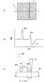
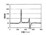
【解決手段】試料表面の観察領域を電子ビームを照射で走査し、観察領域の斜め上方に配置された検出器99aによる二次電子の検出信号に基づいて画像(SEM画像)を取得し、その画像に現れるパターン82の影の長さLを検出する。そして、あらかじ求めた検出器99aの試料表面に対する見掛け上の角度θと検出された影の長さLとに基づいて、パターン82の高さHをH=L×tanθにより求める。パターン82の影の長さLは、例えばパターン82のエッジ82a、82bと直交するラインX−X上の二次電子の強度分布を抽出し、その二次電子の強度分布の凹部が所定のしきい値Iと交差する2点間の距離として求める。
【選択図】図5
Description
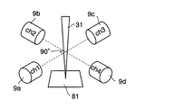
図1は、第1の実施形態に係るパターン高さ測定装置を示すブロック図であり、図2は同じくパターン高さ測定装置の検出器の配置を示す模式図である。
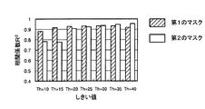
実験例1では、影の長さを検出する際に用いるしきい値Iが測定精度に及ぼす影響について調べた。
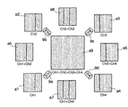
実験例2では、図9に示す第1のマスク50及び第2のマスク60について、影の長さから求めたパターンの高さと、AFMで求めたパターン高さとの相関を調べた。なお、本実験例において、影の長さは第1の方法で求めるものとし、その際のしきい値は25(平坦部の輝度の50%)とした。
上記の説明において、演算部13は、影の長さLにtanθを乗ずることによりパターンの高さHを求めているが、これに代えて、本変形例のように影の長さLに一定のオフセット値Loffを加算してパターンの高さHを求めてもよい。
実験例3では、第1の実施形態の変形例の方法でパターン高さを求めた例について説明する。
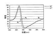
第2の実施形態では、パターンの側壁の傾斜角の影響を考慮した影の長さの検出方法について説明する。なお、本実施形態において、影の長さの検出方法以外は第1の実施形態と同様であるので、共通する部分の説明は省略する。
実験例4では、図16の測定の際に取得した画像データに基づいて、第4の方法で影の長さを検出し直し、影の長さの側壁傾斜角依存性を調べた。
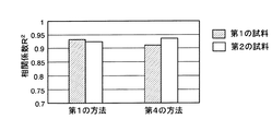
実験例5では、図9に示す第1のマスク50及び第2のマスク60の影の長さを第1の方法及び第4の方法でそれぞれ検出した結果と、AFMによる測定結果との相関を検証した。
実験例6では、第4の方法で検出した影の長さに基づいて、図9に示す第1のマスク50及び第2のマスク60のパターンの高さを測定した。
Claims (20)
- 電子ビームを試料表面に照射つつ走査させる電子ビーム走査部と、
前記試料表面の上方に配置され、前記電子ビームの照射によって前記試料の表面から放出される二次電子の強度を検出する検出器と、
前記検出器の検出信号に基づいて前記試料表面を写した画像データを生成する信号処理部と、
前記画像データに基づいて前記試料表面に形成されたパターンのエッジと交差するラインに沿った二次電子の強度分布を抽出し、前記エッジ付近の二次電子の強度分布に基づいて前記パターンの影の長さを検出する画像処理部と、
前記画像処理部で検出した前記影の長さに基づいて前記パターンの高さを算出する演算部と、
を備えたことを特徴とするパターン高さ測定装置。 - 前記検出器は前記電子ビームの光軸の周りに複数配置され、前記信号処理部は前記複数の検出器からの検出信号に基づいて前記試料表面をそれぞれ異なる方向から写した複数の画像データを生成することを特徴とする請求項1に記載のパターン高さ測定装置。
- 前記画像処理部は、前記パターンのエッジに直交する方向から写した画像データから前記二次電子の強度分布を抽出することを特徴とする請求項2に記載のパターン高さ測定装置。
- 前記画像処理部は、前記エッジ付近の二次電子の強度分布と所定のしきい値とが交差する2点間の距離を前記影の長さとして検出することを特徴とする請求項1乃至請求項3のいずれか1項に記載のパターン高さ測定装置。
- 前記画像処理部は、前記エッジ付近の二次電子の強度分布と所定のしきい値とが前記パターンから離れた側で交差する点と前記二次電子の強度分布の極小値部分との距離を前記影の長さとして検出することを特徴とする請求項1乃至請求項3のいずれか1項に記載のパターン高さ測定装置。
- 前記画像処理部は、前記エッジ付近の二次電子の強度分布と所定のしきい値を表す直線とに囲まれた領域の面積の平方根を影の長さとして検出することを特徴とする請求項1乃至請求項3のいずれか1項に記載のパターン高さ測定装置。
- 前記画像処理部は、前記エッジ付近の二次電子の強度分布と所定のしきい値とが前記パターンから離れた側で交差する点と、前記パターンのエッジの上端又は下端との距離を影の長さとして検出することを特徴とする請求項1乃至3のいずれか1項に記載のパターン高さ測定装置。
- 前記しきい値は、前記エッジ付近の二次電子の強度分布の極小値よりも高く、前記二次電子の強度分布の平坦部の二次電子の強度よりも低い範囲で設定されることを特徴とする請求項4乃至請求項7のいずれか1項に記載のパターン高さ測定装置。
- 前記演算部は、前記検出器の試料表面に対する見かけ上の角度と、前記影の長さとに基づいて、前記パターンの高さを算出することを特徴とする請求項1乃至請求項8のいずれか1項に記載のパターン高さ測定装置。
- 前記演算部は、前記試料の表面の材料によって決まる所定のオフセット値を前記影の長さに加算することにより、前記パターンの高さを算出することを特徴とする請求項1乃至請求項8のいずれか1項に記載のパターン高さ測定装置。
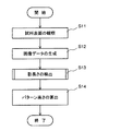
- 電子ビームを試料の表面に照射しつつ走査させるとともに、前記電子ビームの照射によって前記試料の表面から放出される二次電子の強度を前記試料表面の上方に配置された検出器で検出するステップと、
前記検出器からの検出信号に基づいて、前記試料表面を写した画像データを生成するステップと、
前記画像データから前記試料表面に形成されたパターンのエッジと交差するラインに沿った二次電子の強度分布を抽出し、該二次電子の強度分布の凹部に基づいて前記パターンの影の長さを検出するステップと、
前記影の長さに基づいて前記パターンの高さを算出するステップと、
を有することを特徴とするパターン高さ測定方法。 - 前記検出器は、前記電子ビームの光軸の周りに複数配置され、前記複数の検出器からの検出信号に基づいて、前記試料表面をそれぞれ異なる方向から写した複数の画像データを生成することを特徴とする請求項11に記載のパターン高さ測定方法。
- 前記二次電子の強度分布は、前記パターンのエッジに直交する方向から写した画像データから抽出することを特徴とする請求項12に記載のパターン高さ測定方法。
- 前記エッジ付近の二次電子の強度分布と所定のしきい値とが交差する2点間の距離を前記影の長さとして検出することを特徴とする請求項11乃至請求項13のいずれか1項に記載のパターン高さ測定方法。
- 前記エッジ付近の二次電子の強度分布と所定のしきい値とが前記パターンから離れた側で交差する点と前記二次電子の強度分布の極小値部分との距離を前記影の長さとして検出することを特徴とする請求項11乃至請求項13のいずれか1項に記載のパターン高さ測定方法。
- 前記エッジ付近の二次電子の強度分布と所定のしきい値を表す直線とに囲まれた領域の面積の平方根を前記影の長さとして検出することを特徴とする請求項11乃至請求項13のいずれか1項に記載のパターン高さ測定方法。
- 前記エッジ付近の二次電子の強度分布と所定のしきい値とが前記パターンから離れた側で交差する点と前記パターンのエッジの上端又は下端との距離を前記影の長さとして検出することを特徴とする請求項11乃至請求項13のいずれか1項に記載のパターン高さ測定方法。
- 前記しきい値は、前記二次電子の強度分布曲線の凹部の極小値よりも高く、前記二次電子の強度分布曲線の凹部に隣接する平坦部の二次電子の強度よりも低い範囲で設定することを特徴とする請求項14乃至請求項17のいずれか1項に記載のパターン高さ測定方法。
- 前記パターンの高さは、前記検出器の試料表面に対する見かけ上の角度と、前記影の長さとに基づいて算出することを特徴とする請求項11乃至請求項18のいずれか1項に記載のパターン高さ測定方法。
- 前記パターンの高さは、前記試料の表面の材料によって決まる所定のオフセット値を前記影の長さに加算して求めることを特徴とする請求項11乃至請求項18のいずれか1項に記載のパターン高さ測定方法。
Priority Applications (5)
| Application Number | Priority Date | Filing Date | Title |
|---|---|---|---|
| JP2011041674A JP5530959B2 (ja) | 2011-02-28 | 2011-02-28 | パターン高さ測定装置及びパターン高さ測定方法 |
| DE102012101391.8A DE102012101391B4 (de) | 2011-02-28 | 2012-02-21 | Strukturhöhenmessgerät und Strukturhöhenmessverfahren |
| TW101105666A TW201250758A (en) | 2011-02-28 | 2012-02-21 | Pattern-height measurement apparatus and pattern-height measurement method |
| KR1020120019979A KR20120098524A (ko) | 2011-02-28 | 2012-02-27 | 패턴 높이 측정 장치 및 패턴 높이 측정 방법 |
| US13/407,521 US8604431B2 (en) | 2011-02-28 | 2012-02-28 | Pattern-height measuring apparatus and pattern-height measuring method |
Applications Claiming Priority (1)
| Application Number | Priority Date | Filing Date | Title |
|---|---|---|---|
| JP2011041674A JP5530959B2 (ja) | 2011-02-28 | 2011-02-28 | パターン高さ測定装置及びパターン高さ測定方法 |
Publications (2)
| Publication Number | Publication Date |
|---|---|
| JP2012177654A true JP2012177654A (ja) | 2012-09-13 |
| JP5530959B2 JP5530959B2 (ja) | 2014-06-25 |
Family
ID=46635313
Family Applications (1)
| Application Number | Title | Priority Date | Filing Date |
|---|---|---|---|
| JP2011041674A Active JP5530959B2 (ja) | 2011-02-28 | 2011-02-28 | パターン高さ測定装置及びパターン高さ測定方法 |
Country Status (5)
| Country | Link |
|---|---|
| US (1) | US8604431B2 (ja) |
| JP (1) | JP5530959B2 (ja) |
| KR (1) | KR20120098524A (ja) |
| DE (1) | DE102012101391B4 (ja) |
| TW (1) | TW201250758A (ja) |
Cited By (3)
| Publication number | Priority date | Publication date | Assignee | Title |
|---|---|---|---|---|
| JP2016057216A (ja) * | 2014-09-11 | 2016-04-21 | 株式会社アドバンテスト | パターン高さ測定装置及びパターン高さ測定方法 |
| WO2016092641A1 (ja) * | 2014-12-10 | 2016-06-16 | 株式会社 日立ハイテクノロジーズ | 高さ測定装置、及び荷電粒子線装置 |
| US10903041B2 (en) | 2018-06-06 | 2021-01-26 | Hitachi High-Tech Corporation | Pattern measuring method, pattern measuring tool and computer readable medium |
Families Citing this family (9)
| Publication number | Priority date | Publication date | Assignee | Title |
|---|---|---|---|---|
| JP5548159B2 (ja) * | 2010-11-05 | 2014-07-16 | 株式会社アドバンテスト | 欠陥レビュー装置及び欠陥レビュー方法 |
| JP5530959B2 (ja) * | 2011-02-28 | 2014-06-25 | 株式会社アドバンテスト | パターン高さ測定装置及びパターン高さ測定方法 |
| KR20150085956A (ko) * | 2014-01-17 | 2015-07-27 | 삼성전자주식회사 | 반도체 소자의 계측 방법, 반도체 계측 시스템, 및 이들을 이용한 반도체 소자의 제조방법 |
| US9372078B1 (en) * | 2014-06-20 | 2016-06-21 | Western Digital (Fremont), Llc | Detecting thickness variation and quantitative depth utilizing scanning electron microscopy with a surface profiler |
| KR101957007B1 (ko) * | 2014-06-30 | 2019-03-11 | 가부시키가이샤 히다치 하이테크놀로지즈 | 패턴 측정 방법 및 패턴 측정 장치 |
| US10636140B2 (en) * | 2017-05-18 | 2020-04-28 | Applied Materials Israel Ltd. | Technique for inspecting semiconductor wafers |
| US11532760B2 (en) | 2017-05-22 | 2022-12-20 | Howmedica Osteonics Corp. | Device for in-situ fabrication process monitoring and feedback control of an electron beam additive manufacturing process |
| WO2019180760A1 (ja) * | 2018-03-19 | 2019-09-26 | 株式会社 日立ハイテクノロジーズ | パターン計測装置、及び計測を実行させるプログラムを記憶する非一時的なコンピュータ可読媒体 |
| EP3597333A1 (en) | 2018-07-19 | 2020-01-22 | Howmedica Osteonics Corporation | System and process for in-process electron beam profile and location analyses |
Citations (3)
| Publication number | Priority date | Publication date | Assignee | Title |
|---|---|---|---|---|
| JP2001110351A (ja) * | 1999-10-05 | 2001-04-20 | Hitachi Ltd | 走査電子顕微鏡 |
| JP2003157790A (ja) * | 2001-11-20 | 2003-05-30 | Advantest Corp | 微細凹凸量測定装置及び走査型電子顕微鏡 |
| JP2009135273A (ja) * | 2007-11-30 | 2009-06-18 | Hitachi High-Technologies Corp | パターン寸法計測方法及び走査電子顕微鏡 |
Family Cites Families (31)
| Publication number | Priority date | Publication date | Assignee | Title |
|---|---|---|---|---|
| GB1195271A (en) * | 1967-02-16 | 1970-06-17 | Cambridge Instr Co Ltd | Electron Beam Apparatus |
| JPH0643885B2 (ja) * | 1984-05-25 | 1994-06-08 | 株式会社日立製作所 | 荷電粒子マイクロプロ−ブ装置 |
| US4588890A (en) * | 1984-12-31 | 1986-05-13 | International Business Machines Corporation | Apparatus and method for composite image formation by scanning electron beam |
| JPS6275206A (ja) * | 1985-09-30 | 1987-04-07 | Hitachi Ltd | 電子ビ−ム測長装置 |
| DE3602366A1 (de) * | 1986-01-27 | 1987-07-30 | Siemens Ag | Verfahren und anordnung zum nachweis der auf einer probe von einem primaeren korpuskularstrahl ausgeloesten sekundaerkorpuskeln |
| US4912313A (en) * | 1987-11-27 | 1990-03-27 | Hitachi Ltd. | Method of measuring surface topography by using scanning electron microscope, and apparatus therefor |
| US5046110A (en) * | 1988-03-25 | 1991-09-03 | Texas Instruments Incorporated | Comparator error filtering for pattern inspector |
| JP2786207B2 (ja) * | 1988-08-26 | 1998-08-13 | 株式会社日立製作所 | 走査型顕微鏡における表面形状算出方法 |
| JP2754096B2 (ja) * | 1991-03-05 | 1998-05-20 | 日本電子テクニクス株式会社 | 電子線による試料表面の状態測定装置 |
| JPH05299048A (ja) | 1992-04-24 | 1993-11-12 | Hitachi Ltd | 電子線装置および走査電子顕微鏡 |
| US5621214A (en) * | 1995-10-10 | 1997-04-15 | Sofield Science Services, Inc. | Radiation beam scanner |
| US5892224A (en) * | 1996-05-13 | 1999-04-06 | Nikon Corporation | Apparatus and methods for inspecting wafers and masks using multiple charged-particle beams |
| JP2001298036A (ja) * | 2000-02-08 | 2001-10-26 | Toshiba Corp | バンプ高さ測定方法、バンプ位置測定方法およびバンプ高さ測定装置、バンプ位置測定装置ならびに半導体装置の製造方法、半導体装置の実装方法 |
| JP3767341B2 (ja) * | 2000-07-21 | 2006-04-19 | 株式会社日立製作所 | 電子線を用いたパターン検査方法及びその装置 |
| WO2002049065A1 (en) * | 2000-12-12 | 2002-06-20 | Ebara Corporation | Electron beam device and semiconductor device production method using the device |
| JP4041742B2 (ja) * | 2001-05-01 | 2008-01-30 | 株式会社荏原製作所 | 電子線装置及び該電子線装置を用いたデバイス製造方法 |
| JP3960544B2 (ja) * | 2002-10-11 | 2007-08-15 | パイオニア株式会社 | ビーム調整用試料、ビーム調整方法及びビーム調整装置 |
| JP4500099B2 (ja) * | 2004-05-06 | 2010-07-14 | 株式会社日立ハイテクノロジーズ | 電子顕微鏡装置システム及び電子顕微鏡装置システムを用いた寸法計測方法 |
| US7067819B2 (en) * | 2004-05-14 | 2006-06-27 | Kla-Tencor Technologies Corp. | Systems and methods for measurement or analysis of a specimen using separated spectral peaks in light |
| JP4695857B2 (ja) * | 2004-08-25 | 2011-06-08 | 株式会社日立ハイテクノロジーズ | 半導体検査方法および半導体検査装置 |
| JP5033310B2 (ja) * | 2005-02-18 | 2012-09-26 | 株式会社日立ハイテクノロジーズ | 検査装置 |
| US7462828B2 (en) * | 2005-04-28 | 2008-12-09 | Hitachi High-Technologies Corporation | Inspection method and inspection system using charged particle beam |
| US7454221B1 (en) * | 2005-07-12 | 2008-11-18 | Hewlett-Packard Development Company, L.P. | Electron tube amplification |
| JP4843319B2 (ja) * | 2006-01-26 | 2011-12-21 | 株式会社日立ハイテクノロジーズ | 走査型電子顕微鏡 |
| JP5271491B2 (ja) * | 2006-10-26 | 2013-08-21 | 株式会社日立ハイテクノロジーズ | 電子線応用装置および試料検査方法 |
| JP4604096B2 (ja) * | 2008-02-29 | 2010-12-22 | 株式会社日立ハイテクノロジーズ | 荷電粒子線装置 |
| US8080790B2 (en) * | 2008-03-05 | 2011-12-20 | Hitachi High-Technologies Corporation | Scanning electron microscope |
| US8350213B2 (en) * | 2010-03-02 | 2013-01-08 | Hermes Microvision Inc. | Charged particle beam detection unit with multi type detection subunits |
| JP5548159B2 (ja) * | 2010-11-05 | 2014-07-16 | 株式会社アドバンテスト | 欠陥レビュー装置及び欠陥レビュー方法 |
| JP5530959B2 (ja) * | 2011-02-28 | 2014-06-25 | 株式会社アドバンテスト | パターン高さ測定装置及びパターン高さ測定方法 |
| JP5530980B2 (ja) * | 2011-06-14 | 2014-06-25 | 株式会社アドバンテスト | パターン測定装置及びパターン測定方法 |
-
2011
- 2011-02-28 JP JP2011041674A patent/JP5530959B2/ja active Active
-
2012
- 2012-02-21 DE DE102012101391.8A patent/DE102012101391B4/de active Active
- 2012-02-21 TW TW101105666A patent/TW201250758A/zh unknown
- 2012-02-27 KR KR1020120019979A patent/KR20120098524A/ko not_active Ceased
- 2012-02-28 US US13/407,521 patent/US8604431B2/en active Active
Patent Citations (3)
| Publication number | Priority date | Publication date | Assignee | Title |
|---|---|---|---|---|
| JP2001110351A (ja) * | 1999-10-05 | 2001-04-20 | Hitachi Ltd | 走査電子顕微鏡 |
| JP2003157790A (ja) * | 2001-11-20 | 2003-05-30 | Advantest Corp | 微細凹凸量測定装置及び走査型電子顕微鏡 |
| JP2009135273A (ja) * | 2007-11-30 | 2009-06-18 | Hitachi High-Technologies Corp | パターン寸法計測方法及び走査電子顕微鏡 |
Cited By (4)
| Publication number | Priority date | Publication date | Assignee | Title |
|---|---|---|---|---|
| JP2016057216A (ja) * | 2014-09-11 | 2016-04-21 | 株式会社アドバンテスト | パターン高さ測定装置及びパターン高さ測定方法 |
| WO2016092641A1 (ja) * | 2014-12-10 | 2016-06-16 | 株式会社 日立ハイテクノロジーズ | 高さ測定装置、及び荷電粒子線装置 |
| US10101150B2 (en) | 2014-12-10 | 2018-10-16 | Hitachi High-Technologies Corporation | Height measurement device and charged particle beam device |
| US10903041B2 (en) | 2018-06-06 | 2021-01-26 | Hitachi High-Tech Corporation | Pattern measuring method, pattern measuring tool and computer readable medium |
Also Published As
| Publication number | Publication date |
|---|---|
| US8604431B2 (en) | 2013-12-10 |
| KR20120098524A (ko) | 2012-09-05 |
| JP5530959B2 (ja) | 2014-06-25 |
| DE102012101391A1 (de) | 2012-08-30 |
| US20120217392A1 (en) | 2012-08-30 |
| TW201250758A (en) | 2012-12-16 |
| DE102012101391B4 (de) | 2025-10-16 |
Similar Documents
| Publication | Publication Date | Title |
|---|---|---|
| JP5530959B2 (ja) | パターン高さ測定装置及びパターン高さ測定方法 | |
| US8779359B2 (en) | Defect review apparatus and defect review method | |
| TWI515427B (zh) | 基於高電子能量的覆蓋誤差測量方法及系統 | |
| JP5530980B2 (ja) | パターン測定装置及びパターン測定方法 | |
| US8258471B2 (en) | Pattern measuring apparatus and pattern measuring method | |
| KR101137045B1 (ko) | 미세 구조체 검사 방법, 미세 구조체 검사 장치, 및 미세 구조체 검사 프로그램 기록 매체 | |
| JP6147868B2 (ja) | パターン測定装置、及びコンピュータプログラム | |
| JP6084888B2 (ja) | 欠陥検査装置及び欠陥検査方法 | |
| TWI567789B (zh) | A pattern measuring condition setting means, and a pattern measuring means | |
| JP6088337B2 (ja) | パターン検査方法及びパターン検査装置 | |
| JP5533045B2 (ja) | 微細パターン測定方法及び微細パターン測定装置 | |
| JP4094327B2 (ja) | パターン計測方法及びパターン計測装置、並びにパターン工程制御方法 | |
| JP5880134B2 (ja) | パターン計測方法およびパターン計測装置 | |
| JP2017102039A (ja) | パターン計測プログラム、パターン計測方法および装置 | |
| JP2010085376A (ja) | 走査型電子顕微鏡を用いたパターン計測方法 | |
| JP4538421B2 (ja) | 荷電粒子線装置 | |
| JP5458625B2 (ja) | 段差測定方法、段差測定装置及び走査型電子顕微鏡装置 | |
| JP4922710B2 (ja) | 電子顕微鏡の分解能評価用試料及び電子顕微鏡の分解能評価方法並びに電子顕微鏡 | |
| JP6356551B2 (ja) | パターン高さ測定装置及びパターン高さ測定方法 | |
| JP4546500B2 (ja) | パターン計測方法及びパターン計測装置、並びにパターン工程制御方法 | |
| JP2017020981A (ja) | パターン測定装置、及びコンピュータープログラム |
Legal Events
| Date | Code | Title | Description |
|---|---|---|---|
| A621 | Written request for application examination |
Free format text: JAPANESE INTERMEDIATE CODE: A621 Effective date: 20130115 |
|
| A977 | Report on retrieval |
Free format text: JAPANESE INTERMEDIATE CODE: A971007 Effective date: 20130621 |
|
| A131 | Notification of reasons for refusal |
Free format text: JAPANESE INTERMEDIATE CODE: A131 Effective date: 20130625 |
|
| A521 | Request for written amendment filed |
Free format text: JAPANESE INTERMEDIATE CODE: A523 Effective date: 20130729 |
|
| TRDD | Decision of grant or rejection written | ||
| A01 | Written decision to grant a patent or to grant a registration (utility model) |
Free format text: JAPANESE INTERMEDIATE CODE: A01 Effective date: 20140408 |
|
| A61 | First payment of annual fees (during grant procedure) |
Free format text: JAPANESE INTERMEDIATE CODE: A61 Effective date: 20140421 |
|
| R150 | Certificate of patent or registration of utility model |
Ref document number: 5530959 Country of ref document: JP Free format text: JAPANESE INTERMEDIATE CODE: R150 |
|
| R250 | Receipt of annual fees |
Free format text: JAPANESE INTERMEDIATE CODE: R250 |
|
| R250 | Receipt of annual fees |
Free format text: JAPANESE INTERMEDIATE CODE: R250 |
|
| R250 | Receipt of annual fees |
Free format text: JAPANESE INTERMEDIATE CODE: R250 |
|
| R250 | Receipt of annual fees |
Free format text: JAPANESE INTERMEDIATE CODE: R250 |
|
| R250 | Receipt of annual fees |
Free format text: JAPANESE INTERMEDIATE CODE: R250 |
|
| S533 | Written request for registration of change of name |
Free format text: JAPANESE INTERMEDIATE CODE: R313533 |
|
| R350 | Written notification of registration of transfer |
Free format text: JAPANESE INTERMEDIATE CODE: R350 |
|
| R250 | Receipt of annual fees |
Free format text: JAPANESE INTERMEDIATE CODE: R250 |
|
| R250 | Receipt of annual fees |
Free format text: JAPANESE INTERMEDIATE CODE: R250 |