JP2012178774A - バイポーラ/ユニポーラ変換回路 - Google Patents
バイポーラ/ユニポーラ変換回路 Download PDFInfo
- Publication number
- JP2012178774A JP2012178774A JP2011041335A JP2011041335A JP2012178774A JP 2012178774 A JP2012178774 A JP 2012178774A JP 2011041335 A JP2011041335 A JP 2011041335A JP 2011041335 A JP2011041335 A JP 2011041335A JP 2012178774 A JP2012178774 A JP 2012178774A
- Authority
- JP
- Japan
- Prior art keywords
- signal
- circuit
- positive
- conversion circuit
- bipolar
- Prior art date
- Legal status (The legal status is an assumption and is not a legal conclusion. Google has not performed a legal analysis and makes no representation as to the accuracy of the status listed.)
- Granted
Links
- 238000006243 chemical reaction Methods 0.000 title claims abstract description 177
- 238000001514 detection method Methods 0.000 claims abstract description 113
- 230000001360 synchronised effect Effects 0.000 claims description 5
- 230000005540 biological transmission Effects 0.000 description 50
- 230000010355 oscillation Effects 0.000 description 19
- 230000007704 transition Effects 0.000 description 9
- 230000000630 rising effect Effects 0.000 description 6
- 238000010586 diagram Methods 0.000 description 5
- 238000000034 method Methods 0.000 description 4
- 230000005856 abnormality Effects 0.000 description 3
- 238000012544 monitoring process Methods 0.000 description 3
- 238000012937 correction Methods 0.000 description 2
- 230000007423 decrease Effects 0.000 description 2
- 230000003247 decreasing effect Effects 0.000 description 2
- 230000006866 deterioration Effects 0.000 description 2
- 238000013459 approach Methods 0.000 description 1
- 238000012986 modification Methods 0.000 description 1
- 230000004048 modification Effects 0.000 description 1
- 238000006467 substitution reaction Methods 0.000 description 1
Images


Landscapes
- Dc Digital Transmission (AREA)
Abstract
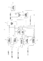
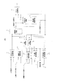
【解決手段】バイポーラ/ユニポーラ変換回路1は、入力信号Iと正極バイアス値V(+)及び負極バイアス値V(−)とを比較し、比較の結果に基づき入力信号をRZ信号に各々変換するRZ変換回路2及び3と、各々のRZ信号の論理和を演算する論理和回路4と、論理和回路4から出力された両極RZ信号AをNRZ信号に変換するNRZ変換回路7と、両極RZ信号に基づき、入力信号の入力状態を検出する入力断検出回路10と、入力断検出回路10の検出結果に基づき、正極及び負極バイアス値を設定するバイアス設定回路12と、各々のRZ信号が所定の符号化規則に従っているか否かを検出する符号則誤り検出回路11とを備え、バイアス設定回路12は、各々のRZ信号が符号化規則に従っていないことが検出された場合に、正極及び負極バイアス値を設定する。
【選択図】図1
Description
2 正極RZ変換回路
3 負極RZ変換回路
4 論理和回路
5 位相比較回路
6 周波数発振回路
7、21 NRZ変換回路
8、22 正極検出回路
9、23 負極検出回路
10 入力断検出回路
11 符号則誤り検出回路
12 バイアス設定回路
31 保護回路
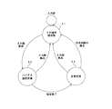
51 入力信号断状態
52 バイアス設定状態
53 定常状態
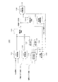
100 バイポーラ/ユニポーラ変換回路
101、102 RZ変換回路
103 論理和回路
104 位相比較回路
105 周波数発振回路
106 NRZ変換回路
107、108 パルス幅検出回路
109 入力断検出回路
110 バイアス設定回路
Claims (7)
- 入力信号と正極バイアス値及び負極バイアス値とを比較し、該比較結果に基づき前記入力信号を正極RZ(Return to Zero)信号及び負極RZ信号の各々に変換する1対のRZ変換手段と、
前記正極RZ信号及び前記負極RZ信号の論理和を演算する論理和演算手段と、
前記論理和演算手段からの出力信号をNRZ(Non Return to Zero)信号に変換するNRZ変換手段と、
前記論理和演算手段からの出力信号に基づき、前記入力信号の入力状態を検出する入力断検出手段と、
前記入力断検出手段の検出結果に基づき、前記正極バイアス値及び前記負極バイアス値を設定するバイアス設定手段と、
前記正極RZ信号及び前記負極RZ信号が所定の符号化規則に従っているか否かを検出する符号則誤り検出手段とを備え、
前記バイアス設定手段は、前記符号則誤り検出手段の検出結果に基づき、前記符号化規則に従っていないことが検出された場合に、前記正極バイアス値及び前記負極バイアス値を設定することを特徴とするバイポーラ/ユニポーラ変換回路。 - 前記正極RZ信号及び前記負極RZ信号のパルス幅を検出し、該パルス幅が所定のパルス幅を超えたか否かを示すエラー信号を各々出力する1対のパルス検出手段をさらに備え、
前記NRZ変換手段は、前記エラー信号に基づき、前記NRZ信号に基づくデータを補正することを特徴とする請求項1に記載のバイポーラ/ユニポーラ変換回路。 - 前記NRZ変換手段は、前記1対のパルス検出手段から出力された各々の前記エラー信号の論理和を演算して得られる結果を反転させた信号と、前記データとの論理積を演算することにより、該データを補正することを特徴とする請求項2に記載のバイポーラ/ユニポーラ変換回路。
- 前記所定のパルス幅は、前記論理和演算手段からの出力信号に同期したクロック信号の1クロック幅であることを特徴とする請求項2又は3に記載のバイポーラ/ユニポーラ変換回路。
- 前記符号則誤り検出手段の検出結果に基づき、所定時間内に前記正極RZ信号及び前記負極RZ信号が前記符号化規則に従っていないことが検出された回数を示すエラー回数をカウントし、該カウント値に応じてエラーを検出したことを示すエラー検出信号を出力する保護手段をさらに備え、
前記バイアス設定手段は、前記エラー検出信号に基づき、前記正極バイアス値及び前記負極バイアス値を設定することを特徴とする請求項1乃至4のいずれかに記載のバイポーラ/ユニポーラ変換回路。 - 前記保護手段は、前記エラー回数のカウント値と、該エラー回数に対して予め設定された閾値とを比較し、前記カウント値が前記閾値を超えた場合に、前記エラー検出信号を出力することを特徴とする請求項5に記載のバイポーラ/ユニポーラ変換回路。
- 前記符号化規則は、B8ZS符号化の規則であることを特徴とする請求項1乃至6のいずれかに記載のバイポーラ/ユニポーラ変換回路。
Priority Applications (1)
| Application Number | Priority Date | Filing Date | Title |
|---|---|---|---|
| JP2011041335A JP5641571B2 (ja) | 2011-02-28 | 2011-02-28 | バイポーラ/ユニポーラ変換回路 |
Applications Claiming Priority (1)
| Application Number | Priority Date | Filing Date | Title |
|---|---|---|---|
| JP2011041335A JP5641571B2 (ja) | 2011-02-28 | 2011-02-28 | バイポーラ/ユニポーラ変換回路 |
Publications (2)
| Publication Number | Publication Date |
|---|---|
| JP2012178774A true JP2012178774A (ja) | 2012-09-13 |
| JP5641571B2 JP5641571B2 (ja) | 2014-12-17 |
Family
ID=46980316
Family Applications (1)
| Application Number | Title | Priority Date | Filing Date |
|---|---|---|---|
| JP2011041335A Expired - Fee Related JP5641571B2 (ja) | 2011-02-28 | 2011-02-28 | バイポーラ/ユニポーラ変換回路 |
Country Status (1)
| Country | Link |
|---|---|
| JP (1) | JP5641571B2 (ja) |
Cited By (1)
| Publication number | Priority date | Publication date | Assignee | Title |
|---|---|---|---|---|
| JP2020162006A (ja) * | 2019-03-27 | 2020-10-01 | Necプラットフォームズ株式会社 | 伝送装置、通信方法、プログラム、および通信システム |
Citations (8)
| Publication number | Priority date | Publication date | Assignee | Title |
|---|---|---|---|---|
| JPS5647144A (en) * | 1979-09-26 | 1981-04-28 | Nec Corp | Signal discriminator |
| JPH04144322A (ja) * | 1990-10-04 | 1992-05-18 | Fujitsu Ltd | 通信誤り検出における監視方式 |
| JPH08139762A (ja) * | 1994-11-11 | 1996-05-31 | Nec Eng Ltd | バイポーラ/ユニポーラ変換回路 |
| JPH09238079A (ja) * | 1996-02-29 | 1997-09-09 | Nec Eng Ltd | バイポーラ・ユニポーラ変換回路 |
| JP2000196684A (ja) * | 1998-12-25 | 2000-07-14 | Nec Corp | 再生中継装置 |
| JP2001045073A (ja) * | 1999-08-02 | 2001-02-16 | Hitachi Ulsi Systems Co Ltd | 三値信号伝達装置 |
| JP2005150889A (ja) * | 2003-11-12 | 2005-06-09 | Nec Engineering Ltd | バイポーラ/ユニポーラ変換回路 |
| JP2006270278A (ja) * | 2005-03-23 | 2006-10-05 | Nec Engineering Ltd | バイポーラ/ユニポーラ変換回路 |
-
2011
- 2011-02-28 JP JP2011041335A patent/JP5641571B2/ja not_active Expired - Fee Related
Patent Citations (8)
| Publication number | Priority date | Publication date | Assignee | Title |
|---|---|---|---|---|
| JPS5647144A (en) * | 1979-09-26 | 1981-04-28 | Nec Corp | Signal discriminator |
| JPH04144322A (ja) * | 1990-10-04 | 1992-05-18 | Fujitsu Ltd | 通信誤り検出における監視方式 |
| JPH08139762A (ja) * | 1994-11-11 | 1996-05-31 | Nec Eng Ltd | バイポーラ/ユニポーラ変換回路 |
| JPH09238079A (ja) * | 1996-02-29 | 1997-09-09 | Nec Eng Ltd | バイポーラ・ユニポーラ変換回路 |
| JP2000196684A (ja) * | 1998-12-25 | 2000-07-14 | Nec Corp | 再生中継装置 |
| JP2001045073A (ja) * | 1999-08-02 | 2001-02-16 | Hitachi Ulsi Systems Co Ltd | 三値信号伝達装置 |
| JP2005150889A (ja) * | 2003-11-12 | 2005-06-09 | Nec Engineering Ltd | バイポーラ/ユニポーラ変換回路 |
| JP2006270278A (ja) * | 2005-03-23 | 2006-10-05 | Nec Engineering Ltd | バイポーラ/ユニポーラ変換回路 |
Cited By (1)
| Publication number | Priority date | Publication date | Assignee | Title |
|---|---|---|---|---|
| JP2020162006A (ja) * | 2019-03-27 | 2020-10-01 | Necプラットフォームズ株式会社 | 伝送装置、通信方法、プログラム、および通信システム |
Also Published As
| Publication number | Publication date |
|---|---|
| JP5641571B2 (ja) | 2014-12-17 |
Similar Documents
| Publication | Publication Date | Title |
|---|---|---|
| US9264219B1 (en) | Clock and data recovery circuit and method | |
| US9558054B2 (en) | Apparatus and method for detecting errors on a transmission path | |
| CN108139998B (zh) | 耐电快速瞬变输入/输出(i/o)通信系统 | |
| US20130272368A1 (en) | Low power data recovery using over-clocking | |
| CN101877623B (zh) | 信号处理器和错误校正处理方法 | |
| US8411811B2 (en) | High jitter and frequency drift tolerant clock data recovery | |
| JP5641571B2 (ja) | バイポーラ/ユニポーラ変換回路 | |
| KR102023796B1 (ko) | 왜곡 내성 클럭 및 데이터 복구 시스템 | |
| JP5326759B2 (ja) | Fsk受信装置、fsk受信方法、及びプログラム | |
| US9331739B1 (en) | System and method for transmitting ancillary data | |
| JP4322946B2 (ja) | 通信装置 | |
| US20150381341A1 (en) | Data receiver and data receiving method thereof | |
| US20120027107A1 (en) | Communication device and communication method in data transmission system | |
| JP2019110491A (ja) | 誤り訂正装置、誤り訂正方法及び光通信システム | |
| JP2015220612A (ja) | 高速シリアル通信用受信回路 | |
| CN106998309A (zh) | 转态强制编码接收器及用于转态强制编码接收器中接收方法 | |
| TWI835597B (zh) | 下降緣調變訊號接收器與下降緣調變訊號取樣方法 | |
| JP2014053755A (ja) | Dcバランスオフセット調整回路およびそれを有する半導体装置 | |
| JP2006270278A (ja) | バイポーラ/ユニポーラ変換回路 | |
| JP2000174838A (ja) | データ受信装置 | |
| WO2016046883A1 (ja) | 受信回路、集積回路及び受信方法 | |
| US8428204B2 (en) | Recovering distorted digital data | |
| JP4617343B2 (ja) | クロックリカバリ回路 | |
| US8847643B2 (en) | Semiconductor device and information processing apparatus | |
| JP2014154190A (ja) | 磁気データ読取装置、監視システム及びエラー検出方法 |
Legal Events
| Date | Code | Title | Description |
|---|---|---|---|
| A621 | Written request for application examination |
Free format text: JAPANESE INTERMEDIATE CODE: A621 Effective date: 20140109 |
|
| A977 | Report on retrieval |
Free format text: JAPANESE INTERMEDIATE CODE: A971007 Effective date: 20140722 |
|
| A131 | Notification of reasons for refusal |
Free format text: JAPANESE INTERMEDIATE CODE: A131 Effective date: 20140729 |
|
| A521 | Request for written amendment filed |
Free format text: JAPANESE INTERMEDIATE CODE: A523 Effective date: 20140910 |
|
| TRDD | Decision of grant or rejection written | ||
| A01 | Written decision to grant a patent or to grant a registration (utility model) |
Free format text: JAPANESE INTERMEDIATE CODE: A01 Effective date: 20141001 |
|
| A61 | First payment of annual fees (during grant procedure) |
Free format text: JAPANESE INTERMEDIATE CODE: A61 Effective date: 20141023 |
|
| R150 | Certificate of patent or registration of utility model |
Ref document number: 5641571 Country of ref document: JP Free format text: JAPANESE INTERMEDIATE CODE: R150 |
|
| S111 | Request for change of ownership or part of ownership |
Free format text: JAPANESE INTERMEDIATE CODE: R313111 |
|
| R350 | Written notification of registration of transfer |
Free format text: JAPANESE INTERMEDIATE CODE: R350 |
|
| LAPS | Cancellation because of no payment of annual fees |