JP2012186099A - 走査電子顕微鏡 - Google Patents
走査電子顕微鏡 Download PDFInfo
- Publication number
- JP2012186099A JP2012186099A JP2011049761A JP2011049761A JP2012186099A JP 2012186099 A JP2012186099 A JP 2012186099A JP 2011049761 A JP2011049761 A JP 2011049761A JP 2011049761 A JP2011049761 A JP 2011049761A JP 2012186099 A JP2012186099 A JP 2012186099A
- Authority
- JP
- Japan
- Prior art keywords
- scanning
- sample
- image
- electron microscope
- orthogonality
- Prior art date
- Legal status (The legal status is an assumption and is not a legal conclusion. Google has not performed a legal analysis and makes no representation as to the accuracy of the status listed.)
- Granted
Links
Images


Classifications
-
- H—ELECTRICITY
- H01—ELECTRIC ELEMENTS
- H01J—ELECTRIC DISCHARGE TUBES OR DISCHARGE LAMPS
- H01J37/00—Discharge tubes with provision for introducing objects or material to be exposed to the discharge, e.g. for the purpose of examination or processing thereof
- H01J37/02—Details
- H01J37/04—Arrangements of electrodes and associated parts for generating or controlling the discharge, e.g. electron-optical arrangement or ion-optical arrangement
- H01J37/147—Arrangements for directing or deflecting the discharge along a desired path
-
- H—ELECTRICITY
- H01—ELECTRIC ELEMENTS
- H01J—ELECTRIC DISCHARGE TUBES OR DISCHARGE LAMPS
- H01J37/00—Discharge tubes with provision for introducing objects or material to be exposed to the discharge, e.g. for the purpose of examination or processing thereof
- H01J37/02—Details
- H01J37/04—Arrangements of electrodes and associated parts for generating or controlling the discharge, e.g. electron-optical arrangement or ion-optical arrangement
- H01J37/153—Electron-optical or ion-optical arrangements for the correction of image defects, e.g. stigmators
-
- H—ELECTRICITY
- H01—ELECTRIC ELEMENTS
- H01J—ELECTRIC DISCHARGE TUBES OR DISCHARGE LAMPS
- H01J37/00—Discharge tubes with provision for introducing objects or material to be exposed to the discharge, e.g. for the purpose of examination or processing thereof
- H01J37/26—Electron or ion microscopes; Electron or ion diffraction tubes
- H01J37/261—Details
- H01J37/265—Controlling the tube; circuit arrangements adapted to a particular application not otherwise provided, e.g. bright-field-dark-field illumination
-
- H—ELECTRICITY
- H01—ELECTRIC ELEMENTS
- H01J—ELECTRIC DISCHARGE TUBES OR DISCHARGE LAMPS
- H01J37/00—Discharge tubes with provision for introducing objects or material to be exposed to the discharge, e.g. for the purpose of examination or processing thereof
- H01J37/26—Electron or ion microscopes; Electron or ion diffraction tubes
- H01J37/28—Electron or ion microscopes; Electron or ion diffraction tubes with scanning beams
-
- H—ELECTRICITY
- H01—ELECTRIC ELEMENTS
- H01J—ELECTRIC DISCHARGE TUBES OR DISCHARGE LAMPS
- H01J2237/00—Discharge tubes exposing object to beam, e.g. for analysis treatment, etching, imaging
- H01J2237/22—Treatment of data
- H01J2237/221—Image processing
Landscapes
- Chemical & Material Sciences (AREA)
- Analytical Chemistry (AREA)
- Electron Sources, Ion Sources (AREA)
- Length-Measuring Devices Using Wave Or Particle Radiation (AREA)
Abstract
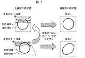
【解決手段】上記目的を達成するために、直交度規定用に格子状サンプルではなく粒子状サンプルを使用し、円であるべき像を円として観察されるような調整を実施することで、直交度を規定することが可能となる。
【選択図】 図1
Description
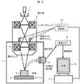
2 コンデンサレンズ
3 走査コイル
4 電子レンズ
5 試料台
6 試料ステージ
7 チャンバー
8 二次電子検出器
9 画像メモリ
10 画像モニタ
11 装置制御部
12 走査コイル制御部
13 直交度調整選択設定画面
14 直交度調整操作画面
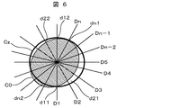
C0 球状試料のSEM観察像
Cz SEM像観察画面上の設定された真円
Dn 真円の中心を通る直線
dni 真円の直径と直線DnがC0のSEM観察像輪郭線と交わる2点間距離の差
Claims (7)
- 電子銃で発生した一次電子線を走査偏向器を用いて試料上に走査して、当該試料の画像を取得する走査電子顕微鏡において、
前記走査偏向器のXY走査方向を調整する制御部と、
前記制御部によるXY走査方向の調整量を求めるコンピュータと、
前記画像を表示するモニタとを備え、
前記コンピュータは、球状試料の実画像の輪郭線上での4点における接線により構成される矩形の一辺が、互いに長さが等しくなるように前記XY走査方向の調整量を求めることを特徴とする走査電子顕微鏡。 - 電子銃で発生した一次電子線を走査偏向器を用いて試料上に走査して、当該試料の画像を取得する走査電子顕微鏡において、
前記走査偏向器のXY走査方向を調整する制御部と、
前記制御部によるXY走査方向の調整量を求めるコンピュータと、
前記画像を表示するモニタとを備え、
前記コンピュータは、球状試料の実画像の輪郭線が、当該コンピュータにより生成された前記球状試料の実画像と面積が等しい真円に一致するように前記XY走査方向の調整量を求めることを特徴とする走査電子顕微鏡。 - 請求項1に記載の走査電子顕微鏡において、
前記モニタ上に、前記球状試料の実画像の輪郭線に対する前記接線の位置を定めるための操作画面が表示されることを特徴とする走査電子顕微鏡。 - 請求項2に記載の走査電子顕微鏡において、
前記モニタ上に、前記球状試料の実画像の輪郭線の中心と前記真円の中心とが重なるように、前記球状試料の実画像の輪郭線または前記真円の表示位置を移動するための操作画面が表示されることを特徴とする走査電子顕微鏡。 - 請求項4に記載の走査電子顕微鏡において、
前記コンピュータは、前記輪郭線の中心を通る直線と前記輪郭線との2交点間の長さと前記真円の直径との差の自乗和を、向きの異なる複数の直線について計算し、
当該自乗和が所定のしきい値よりも小さくなるように前記XY走査方向の調整量を求めることを特徴とする走査電子顕微鏡。 - 電子銃で発生した一次電子線を走査偏向器を用いて試料上のXY方向に走査して、当該試料の画像を取得する走査電子顕微鏡の走査偏向器の調整方法において、
球状試料の実画像の輪郭線上での4点における接線により構成される矩形の一辺が、互いに長さが等しくなるようにXY走査方向の調整量を求めることを特徴とする走査偏向器の調整方法。 - 電子銃で発生した一次電子線を走査偏向器を用いて試料上のXY方向に走査して、当該試料の画像を取得する走査電子顕微鏡の走査偏向器の調整方法において、
球状試料の実画像の輪郭線が、当該コンピュータにより生成された前記球状試料の実画像と面積が等しい真円に一致するようにXY走査方向の調整量を求めることを特徴とする走査電子顕微鏡の調整方法。
Priority Applications (4)
| Application Number | Priority Date | Filing Date | Title |
|---|---|---|---|
| JP2011049761A JP5581248B2 (ja) | 2011-03-08 | 2011-03-08 | 走査電子顕微鏡 |
| DE112011104697T DE112011104697T5 (de) | 2011-03-08 | 2011-11-11 | Rasterelektronenmikroskop |
| US13/981,685 US8927931B2 (en) | 2011-03-08 | 2011-11-11 | Scanning electron microscope |
| PCT/JP2011/006307 WO2012120576A1 (ja) | 2011-03-08 | 2011-11-11 | 走査電子顕微鏡 |
Applications Claiming Priority (1)
| Application Number | Priority Date | Filing Date | Title |
|---|---|---|---|
| JP2011049761A JP5581248B2 (ja) | 2011-03-08 | 2011-03-08 | 走査電子顕微鏡 |
Publications (2)
| Publication Number | Publication Date |
|---|---|
| JP2012186099A true JP2012186099A (ja) | 2012-09-27 |
| JP5581248B2 JP5581248B2 (ja) | 2014-08-27 |
Family
ID=46797588
Family Applications (1)
| Application Number | Title | Priority Date | Filing Date |
|---|---|---|---|
| JP2011049761A Expired - Fee Related JP5581248B2 (ja) | 2011-03-08 | 2011-03-08 | 走査電子顕微鏡 |
Country Status (4)
| Country | Link |
|---|---|
| US (1) | US8927931B2 (ja) |
| JP (1) | JP5581248B2 (ja) |
| DE (1) | DE112011104697T5 (ja) |
| WO (1) | WO2012120576A1 (ja) |
Cited By (2)
| Publication number | Priority date | Publication date | Assignee | Title |
|---|---|---|---|---|
| JP2018195545A (ja) * | 2017-05-22 | 2018-12-06 | 日本電子株式会社 | 荷電粒子線装置および走査像の歪み補正方法 |
| JP7299206B2 (ja) | 2017-02-16 | 2023-06-27 | 株式会社荏原製作所 | 電子ビームの照射エリア調整方法および同調整システム、電子ビームの照射領域補正方法、ならびに、電子ビーム照射装置 |
Families Citing this family (2)
| Publication number | Priority date | Publication date | Assignee | Title |
|---|---|---|---|---|
| WO2015045468A1 (ja) * | 2013-09-30 | 2015-04-02 | 株式会社日立ハイテクノロジーズ | 荷電粒子ビーム装置 |
| US11062875B2 (en) * | 2019-10-14 | 2021-07-13 | City University Of Hong Kong | Imaging apparatus and related control unit |
Citations (4)
| Publication number | Priority date | Publication date | Assignee | Title |
|---|---|---|---|---|
| JPH05190130A (ja) * | 1992-01-13 | 1993-07-30 | Nikon Corp | 電子顕微鏡の電子ビーム偏向磁場調整方法 |
| JPH0721961A (ja) * | 1993-07-05 | 1995-01-24 | Hitachi Ltd | 透過電子顕微鏡用又は電子エネルギー損失分析電子顕微鏡用の撮像方法及び撮像装置 |
| JP2007179753A (ja) * | 2005-12-27 | 2007-07-12 | Hitachi High-Technologies Corp | 走査透過電子顕微鏡、及び収差測定方法 |
| JP2008171756A (ja) * | 2007-01-15 | 2008-07-24 | Jeol Ltd | 電子顕微鏡の歪み測定方法及び輝度補正方法 |
Family Cites Families (19)
| Publication number | Priority date | Publication date | Assignee | Title |
|---|---|---|---|---|
| JPS63150842A (ja) | 1986-12-15 | 1988-06-23 | Nichidenshi Tekunikusu:Kk | 走査電子顕微鏡 |
| US5923430A (en) * | 1993-06-17 | 1999-07-13 | Ultrapointe Corporation | Method for characterizing defects on semiconductor wafers |
| JP3256678B2 (ja) * | 1998-02-19 | 2002-02-12 | 株式会社東芝 | レンズの収差測定方法 |
| US6248486B1 (en) * | 1998-11-23 | 2001-06-19 | U.S. Philips Corporation | Method of detecting aberrations of an optical imaging system |
| US6368763B2 (en) * | 1998-11-23 | 2002-04-09 | U.S. Philips Corporation | Method of detecting aberrations of an optical imaging system |
| JP3987276B2 (ja) * | 2000-10-12 | 2007-10-03 | 株式会社日立製作所 | 試料像形成方法 |
| US6770867B2 (en) * | 2001-06-29 | 2004-08-03 | Fei Company | Method and apparatus for scanned instrument calibration |
| JP3968334B2 (ja) * | 2002-09-11 | 2007-08-29 | 株式会社日立ハイテクノロジーズ | 荷電粒子線装置及び荷電粒子線照射方法 |
| US7136143B2 (en) * | 2002-12-13 | 2006-11-14 | Smith Bruce W | Method for aberration detection and measurement |
| JP4248387B2 (ja) * | 2003-12-17 | 2009-04-02 | 日本電子株式会社 | 収差自動補正方法及び装置 |
| JP2005183085A (ja) * | 2003-12-17 | 2005-07-07 | Jeol Ltd | 収差自動補正方法及び装置 |
| JP4351108B2 (ja) * | 2004-04-07 | 2009-10-28 | 日本電子株式会社 | Semの収差自動補正方法及び収差自動補正装置 |
| JP4522203B2 (ja) * | 2004-09-14 | 2010-08-11 | 日本電子株式会社 | 荷電粒子ビーム装置の色収差補正方法及び装置並びに荷電粒子ビーム装置 |
| JP5078431B2 (ja) * | 2007-05-17 | 2012-11-21 | 株式会社日立ハイテクノロジーズ | 荷電粒子ビーム装置、その収差補正値算出装置、及びその収差補正プログラム |
| DE102008035297B4 (de) * | 2007-07-31 | 2017-08-17 | Hitachi High-Technologies Corporation | Aberrationskorrektureinrichtung für Ladungsteilchenstrahlen in einem optischen System einer Ladungsteilchenstrahlvorrichtung und Ladungsteilchenstrahlvorrichtung mit der Aberrationskorrektureinrichtung |
| TWI479570B (zh) * | 2007-12-26 | 2015-04-01 | 奈華科技有限公司 | 從樣本移除材料之方法及系統 |
| JP5277250B2 (ja) * | 2008-09-25 | 2013-08-28 | 株式会社日立ハイテクノロジーズ | 荷電粒子線応用装置およびその幾何収差測定方法 |
| JP5350123B2 (ja) * | 2009-08-10 | 2013-11-27 | 株式会社日立ハイテクノロジーズ | 荷電粒子線装置及び画像表示方法 |
| EP2534667A2 (en) * | 2010-02-10 | 2012-12-19 | Mochii, Inc. (d/b/a Voxa) | Aberration-correcting dark-field electron microscopy |
-
2011
- 2011-03-08 JP JP2011049761A patent/JP5581248B2/ja not_active Expired - Fee Related
- 2011-11-11 DE DE112011104697T patent/DE112011104697T5/de not_active Withdrawn
- 2011-11-11 US US13/981,685 patent/US8927931B2/en not_active Expired - Fee Related
- 2011-11-11 WO PCT/JP2011/006307 patent/WO2012120576A1/ja not_active Ceased
Patent Citations (4)
| Publication number | Priority date | Publication date | Assignee | Title |
|---|---|---|---|---|
| JPH05190130A (ja) * | 1992-01-13 | 1993-07-30 | Nikon Corp | 電子顕微鏡の電子ビーム偏向磁場調整方法 |
| JPH0721961A (ja) * | 1993-07-05 | 1995-01-24 | Hitachi Ltd | 透過電子顕微鏡用又は電子エネルギー損失分析電子顕微鏡用の撮像方法及び撮像装置 |
| JP2007179753A (ja) * | 2005-12-27 | 2007-07-12 | Hitachi High-Technologies Corp | 走査透過電子顕微鏡、及び収差測定方法 |
| JP2008171756A (ja) * | 2007-01-15 | 2008-07-24 | Jeol Ltd | 電子顕微鏡の歪み測定方法及び輝度補正方法 |
Cited By (2)
| Publication number | Priority date | Publication date | Assignee | Title |
|---|---|---|---|---|
| JP7299206B2 (ja) | 2017-02-16 | 2023-06-27 | 株式会社荏原製作所 | 電子ビームの照射エリア調整方法および同調整システム、電子ビームの照射領域補正方法、ならびに、電子ビーム照射装置 |
| JP2018195545A (ja) * | 2017-05-22 | 2018-12-06 | 日本電子株式会社 | 荷電粒子線装置および走査像の歪み補正方法 |
Also Published As
| Publication number | Publication date |
|---|---|
| JP5581248B2 (ja) | 2014-08-27 |
| US8927931B2 (en) | 2015-01-06 |
| DE112011104697T5 (de) | 2013-10-10 |
| WO2012120576A1 (ja) | 2012-09-13 |
| US20130306864A1 (en) | 2013-11-21 |
Similar Documents
| Publication | Publication Date | Title |
|---|---|---|
| JP5156619B2 (ja) | 試料寸法検査・測定方法、及び試料寸法検査・測定装置 | |
| US10417756B2 (en) | Pattern measurement apparatus and defect inspection apparatus | |
| JP4627782B2 (ja) | エッジ検出方法、及び荷電粒子線装置 | |
| TWI464394B (zh) | Defect detection device | |
| WO2013118613A1 (ja) | パターン評価方法およびパターン評価装置 | |
| JP4791141B2 (ja) | 電子線式寸法計測装置及びそれを用いた寸法計測方法 | |
| CN115507782A (zh) | 图案测量装置及图案测量方法 | |
| JP6147868B2 (ja) | パターン測定装置、及びコンピュータプログラム | |
| JP2009252959A (ja) | パターン検査装置、パターン検査方法および半導体装置の製造方法 | |
| JP2008292472A (ja) | 欠陥観察装置、および欠陥観察方法 | |
| US20230222764A1 (en) | Image processing method, pattern inspection method, image processing system, and pattern inspection system | |
| JP5581248B2 (ja) | 走査電子顕微鏡 | |
| JP2007232387A (ja) | 検査装置、および検査方法 | |
| JPWO2010061516A1 (ja) | 画像形成方法、及び画像形成装置 | |
| JP5564276B2 (ja) | パターンマッチング用画像作成装置 | |
| JP6850234B2 (ja) | 荷電粒子線装置 | |
| US10276341B2 (en) | Control method and control program for focused ion beam device | |
| JP5094033B2 (ja) | パターンマッチング方法、及びパターンマッチングを行うためのコンピュータープログラム | |
| JP5171071B2 (ja) | 撮像倍率調整方法及び荷電粒子線装置 | |
| JP2011179819A (ja) | パターン測定方法及びコンピュータプログラム | |
| JP6078356B2 (ja) | テンプレートマッチング条件設定装置、及び荷電粒子線装置 | |
| JP6207893B2 (ja) | 試料観察装置用のテンプレート作成装置 | |
| WO2012056639A1 (ja) | パターンの判定装置、及びコンピュータプログラム | |
| WO2026023005A1 (ja) | データセット生成装置、データセット生成方法、撮像装置、撮像方法、顕微鏡装置、データセット生成システム、撮像システムおよび半導体デバイス製造システム | |
| CN121488320A (zh) | 具有检查测量模型的扫描型电子显微镜及检查测量模型的修正方法 |
Legal Events
| Date | Code | Title | Description |
|---|---|---|---|
| A621 | Written request for application examination |
Free format text: JAPANESE INTERMEDIATE CODE: A621 Effective date: 20130201 |
|
| A521 | Request for written amendment filed |
Free format text: JAPANESE INTERMEDIATE CODE: A523 Effective date: 20130201 |
|
| A131 | Notification of reasons for refusal |
Free format text: JAPANESE INTERMEDIATE CODE: A131 Effective date: 20140121 |
|
| TRDD | Decision of grant or rejection written | ||
| A01 | Written decision to grant a patent or to grant a registration (utility model) |
Free format text: JAPANESE INTERMEDIATE CODE: A01 Effective date: 20140617 |
|
| A61 | First payment of annual fees (during grant procedure) |
Free format text: JAPANESE INTERMEDIATE CODE: A61 Effective date: 20140714 |
|
| R150 | Certificate of patent or registration of utility model |
Ref document number: 5581248 Country of ref document: JP Free format text: JAPANESE INTERMEDIATE CODE: R150 |
|
| LAPS | Cancellation because of no payment of annual fees |