WO2012120576A1 - 走査電子顕微鏡 - Google Patents
走査電子顕微鏡 Download PDFInfo
- Publication number
- WO2012120576A1 WO2012120576A1 PCT/JP2011/006307 JP2011006307W WO2012120576A1 WO 2012120576 A1 WO2012120576 A1 WO 2012120576A1 JP 2011006307 W JP2011006307 W JP 2011006307W WO 2012120576 A1 WO2012120576 A1 WO 2012120576A1
- Authority
- WO
- WIPO (PCT)
- Prior art keywords
- scanning
- sample
- image
- electron microscope
- spherical
- Prior art date
- Legal status (The legal status is an assumption and is not a legal conclusion. Google has not performed a legal analysis and makes no representation as to the accuracy of the status listed.)
- Ceased
Links
Images



Classifications
-
- H—ELECTRICITY
- H01—ELECTRIC ELEMENTS
- H01J—ELECTRIC DISCHARGE TUBES OR DISCHARGE LAMPS
- H01J37/00—Discharge tubes with provision for introducing objects or material to be exposed to the discharge, e.g. for the purpose of examination or processing thereof
- H01J37/02—Details
- H01J37/04—Arrangements of electrodes and associated parts for generating or controlling the discharge, e.g. electron-optical arrangement or ion-optical arrangement
- H01J37/147—Arrangements for directing or deflecting the discharge along a desired path
-
- H—ELECTRICITY
- H01—ELECTRIC ELEMENTS
- H01J—ELECTRIC DISCHARGE TUBES OR DISCHARGE LAMPS
- H01J37/00—Discharge tubes with provision for introducing objects or material to be exposed to the discharge, e.g. for the purpose of examination or processing thereof
- H01J37/02—Details
- H01J37/04—Arrangements of electrodes and associated parts for generating or controlling the discharge, e.g. electron-optical arrangement or ion-optical arrangement
- H01J37/153—Electron-optical or ion-optical arrangements for the correction of image defects, e.g. stigmators
-
- H—ELECTRICITY
- H01—ELECTRIC ELEMENTS
- H01J—ELECTRIC DISCHARGE TUBES OR DISCHARGE LAMPS
- H01J37/00—Discharge tubes with provision for introducing objects or material to be exposed to the discharge, e.g. for the purpose of examination or processing thereof
- H01J37/26—Electron or ion microscopes; Electron or ion diffraction tubes
- H01J37/261—Details
- H01J37/265—Controlling the tube; circuit arrangements adapted to a particular application not otherwise provided, e.g. bright-field-dark-field illumination
-
- H—ELECTRICITY
- H01—ELECTRIC ELEMENTS
- H01J—ELECTRIC DISCHARGE TUBES OR DISCHARGE LAMPS
- H01J37/00—Discharge tubes with provision for introducing objects or material to be exposed to the discharge, e.g. for the purpose of examination or processing thereof
- H01J37/26—Electron or ion microscopes; Electron or ion diffraction tubes
- H01J37/28—Electron or ion microscopes; Electron or ion diffraction tubes with scanning beams
-
- H—ELECTRICITY
- H01—ELECTRIC ELEMENTS
- H01J—ELECTRIC DISCHARGE TUBES OR DISCHARGE LAMPS
- H01J2237/00—Discharge tubes exposing object to beam, e.g. for analysis treatment, etching, imaging
- H01J2237/22—Treatment of data
- H01J2237/221—Image processing
Definitions
- the present invention relates to an electron microscope, and in particular, provides an electron microscope having a function of automatically correcting the orthogonality by calculating the orthogonality and reflecting the calculated result in the deflection control circuit.
- the scanning electron microscope scans two-dimensionally in the XY plane on the sample on which the primary electron beam is to be observed, detects secondary electrons or backscattered electrons generated from the scanning position, and outputs the detector output signal.
- This is an apparatus for obtaining an observation image of a target sample by imaging. Since secondary electrons and reflected electrons are generated along the scanning trajectory of the primary electron beam, the obtained image is naturally distorted if the X scanning direction and the Y scanning direction are not orthogonal.
- FIG. 1 shows the relationship between the orthogonality of scanning lines to the scanning area and image distortion. If the scanning region in the X direction and the scanning region in the Y direction are not appropriate, the image is observed with distortion as shown in FIG. FIG. 1 shows an example of a circular sample as an observation object. For example, when the scanning region is distorted in a diamond shape, the observed image is observed in an elliptical shape. When the scanning area is appropriately a square area, a circular object is correctly observed as a circular image.
- the degree of orthogonality between the X scanning line and the Y scanning line is generally referred to as orthogonality, but in an actual scanning electron microscope, the orthogonality is adjusted to such an extent that the X scanning line and the Y scanning line can be regarded as orthogonal. There is a need.
- Patent Document 1 discloses an invention in which an SEM image is divided into a lattice shape, a lattice-like sheet is pasted on a monitor, and the deflection distortion for each divided region is visually adjusted.
- the lattice-shaped sample has a manufacturing accuracy variation and is visually adjusted, there is a problem in the conventional technique that the orthogonality after the adjustment may vary for each electron microscope. . Further, since the correction value of the control circuit is manually input, there is a problem that the correction accuracy varies. Furthermore, when a single user uses a plurality of electron microscopes, there is a case where a difference in orthogonality between the electron microscopes becomes obvious and becomes a problem.
- An object of the present invention is to realize an electron microscope adjustment method with less variation in orthogonality than before and an electron microscope having a function of executing the adjustment method.
- a spherical sample that is considered to have less manufacturing variation than the lattice-like sample is used, and an algorithm that defines the orthogonality from the image of the spherical sample is adopted.
- the correction value of the control circuit of the electron microscope is calculated and automatically set in the control sequencer of the deflector.
- the present invention it is not necessary to manufacture a lattice-shaped sample, and it becomes easy to reduce the variation in the orthogonality by defining the orthogonality from the spherical sample.
- a function that can be automatically determined it is possible to reduce the variation of regulations by people. As a result, it is possible to reduce variations among apparatuses and to obtain an effect of improving the performance of the apparatus.
- FIG. 6 is a diagram illustrating the relationship between the orthogonality of scanning lines to a scanning region and image distortion.
- FIG. 3 is a diagram illustrating an adjustment principle of an adjustment algorithm of a scanning deflector according to the first embodiment.
- FIG. 6 is a diagram illustrating an adjustment flow of the scanning deflector according to the first embodiment. 6 is an operation screen used for adjusting the scanning deflector according to the first embodiment.
- FIG. 6 is a diagram illustrating an adjustment principle of an adjustment algorithm of a scanning deflector according to a second embodiment.
- FIG. 10 is a diagram illustrating an adjustment flow of the scanning deflector according to the second embodiment.
- a particulate sample is used for an apparatus for observing an SEM image, and the accuracy at the time of measuring the orthogonality of the apparatus is defined by using the spherical characteristic.
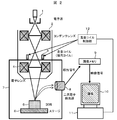
- FIG. 2 shows the configuration of the scanning electron microscope of this example. Electrons are accelerated and extracted from the electron gun 1, the electron probe is condensed by the condenser lens 2, the focus is adjusted by the electron lens 4, and the sample on the sample stage 5 is irradiated with electrons.
- the electronic probe is located between the condenser lens 2 and the electronic lens 4 and has a structure in which the position can be changed by the scanning coil 3 (scanning deflector).
- the scanning coil 3 includes an X deflection coil that adjusts distortion in the horizontal direction (X direction) of the observation image and a Y deflection coil that adjusts distortion in the vertical direction (Y direction) of the observation image.
- the distortion-free image is realized by adjusting the current value.
- the sample stage 5 is transported and mounted on the sample stage 6 by a transport mechanism (not shown).
- the sample stage 5, the sample stage 6 and others are housed in a chamber 7, and the chamber 7 is kept in a vacuum state by a vacuum exhaust device (not shown).
- Secondary electrons are emitted from the sample by the electrons irradiated on the sample on the sample stage 5, detected by the secondary electron detector 8, and the detection signal is displayed on the image monitor 10 via the image memory 9. Observed as a secondary electron image.
- the image monitor 10 is connected to the apparatus control unit 11.
- the apparatus control unit 11 is often realized by a personal computer-based arithmetic unit. In addition to the calculation of the correction value of the orthogonality set in the scanning coil control unit 12, the host control unit controls the entire scanning electron microscope. Function as.
- the device control unit 11 is connected to input devices such as a mouse and a keyboard.
- a spherical sample is mounted on the sample on the sample stage 5, and an SEM image of the spherical sample is acquired by observing the secondary electron image of the spherical sample. .
- the apparatus control unit 11 calculates the current correction value of the scanning coil 3 using the SEM image of the spherical sample.
- the scanning coil control unit 12 (deflection control sequencer) includes a storage element such as a latch circuit or a register, and stores the calculated current correction value.
- the scanning coil controller 12 adjusts the orthogonal relationship between the X scanning line and the Y scanning line using the current correction value.
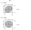
- FIG. 3 shows the principle of the orthogonality adjustment algorithm of this embodiment.
- the scanning coil control unit 12 is adjusted so that the length of one side of the rectangle formed by the tangents at the four points on the outline of the real image of the spherical sample is equal to the length of the other side, the orthogonality can be increased. It can be adjusted appropriately.
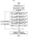
- FIG. 4 shows an adjustment flow of the scanning deflector of this embodiment.
- the orthogonality in the Y direction with respect to the X direction has been adjusted using a lattice-like sample for defining the orthogonality.
- the orthogonality is defined by using a spherical sample instead of the lattice sample.
- a spherical sample is mounted on a sample stage of a scanning electron microscope, and is transported into a sample chamber using a sample stage.
- the spherical sample include polystyrene latex particles (usually PSL particles). Polystyrene latex particles are known as true spherical particles with very uniform particle sizes. However, the spherical sample that can be used is not limited to this.
- a secondary electron image or a reflected electron image of the spherical sample is acquired, and an image is displayed on the operation screen for adjusting the orthogonality displayed on the image monitor 10.
- a selection button for displaying the operation screen is displayed. When the device user presses this button, the orthogonality adjustment shown in FIG. The selection setting screen is displayed.
- the adjustment of the orthogonality can be both automatically executed by the device control unit 11 and manually adjusted by the device user, and the Auto ADJ. Or Manual ADJ.
- the orthogonality adjustment operation screen shown in FIG. 5B is displayed, and the adjustment flow is started thereafter.
- an acquired image in which the orthogonality is in various fabric states is displayed on the orthogonality adjustment operation screen in FIG.
- the X cross cursor and the Y cross cursor indicated by the four straight lines in FIG. 3A are displayed on the orthogonality adjustment operation screen.
- an elliptical image as shown in FIG. 3A is observed even for a spherical sample.
- the XY cross cursor is a straight line generated by the apparatus control unit 11, it can be regarded as two straight lines that completely intersect at 90 degrees on the screen.
- the operator first searches the screen for a position where the straight line in the X direction of the X cross cursor contacts the lower side of the ellipse on the observation image, and records the Y position coordinate Y1 of the cursor at this time. Similarly, the position where the straight line in the X direction of the second X cross cursor touches the upper side of the ellipse on the observation image, the position where the straight line in the Y direction of the first Y cross cursor touches the left side of the observation image ellipse, and the second Y The position where the straight line in the Y direction of the cross cursor touches the right side of the observation image ellipse is searched, and the position coordinates of each cursor, that is, the Y position coordinates Y2, the X position coordinates X1, and the X position coordinates X2 are recorded. The position coordinates are automatically recorded in the apparatus control unit 11 by, for example, a double click operation of the mouse.
- the distance B in the Y direction is calculated as Y2 ⁇ Y1.
- the step size (increment) when changing the X coil and Y coil current values is stored in the main body control unit 11 and the scanning coil control unit 12. The operator may be able to set step size information via an appropriate setting screen.
- the apparatus control unit 11 transfers the current values of the X coil and Y coil at this time to the scanning coil control unit 12 as correction values.
- the scanning coil control unit 12 stores the transferred correction value in an internal storage element.
- the coordinates X1, X2, Y1, and Y2 are set manually, but the adjustment flow shown in FIG. 4 can be easily automated. However, since it is better for the final adjustment result to be confirmed by a person, even if automatic execution is selected in FIG. 5A, the final result is displayed in FIG. 5B. The device user visually confirms.
- the orthogonality obtained as a result of the automatic execution can be measured with reference to the cross cursor on the screen, and it can be determined that the adjustment of the orthogonality is completed by observing the display image as a circle.
- FIG. 6 shows the principle of the adjustment algorithm of this embodiment. Considering a perfect circle Cz having the same area as the observation image C0 and the observation image C0 of the spherical sample, if the orthogonality is within a specified value, they should match.
- the correction value of the straightness is obtained by obtaining the current values of the X deflection coil and the Y deflection coil such that they match.
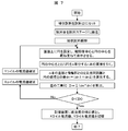
- FIG. 7 shows an adjustment flow of the scanning deflector according to the second embodiment.
- a plurality of straight lines (for example, n lines) passing through the center of the circle are arranged on the perfect circle Cz so as to divide the true circle Cz into n equal parts.
- These straight lines are defined as straight lines Dn, and the sum of squares of the difference dni between the length of the intersection between the contour line of the observation image C0 of the spherical sample and the straight line Dn and the diameter of the perfect circle is calculated for each of the straight lines Dn. D is obtained.
- the reason why the sum of squares is used is that a deviation from the perfect circle Cz of the observation image C0 is not correctly expressed by a positive or negative sign in the sum of simple differences.
- the threshold D0 and the increments of the X coil and Y coil current values are stored in the main body control unit 11 and the scanning coil control unit 12. The operator may be able to set the above information via an appropriate setting screen.
Landscapes
- Chemical & Material Sciences (AREA)
- Analytical Chemistry (AREA)
- Electron Sources, Ion Sources (AREA)
- Length-Measuring Devices Using Wave Or Particle Radiation (AREA)
Abstract
Description
2 コンデンサレンズ
3 走査コイル
4 電子レンズ
5 試料台
6 試料ステージ
7 チャンバー
8 二次電子検出器
9 画像メモリ
10 画像モニタ
11 装置制御部
12 走査コイル制御部
13 直交度調整選択設定画面
14 直交度調整操作画面
C0 球状試料のSEM観察像
Cz SEM像観察画面上の設定された真円
Dn 真円の中心を通る直線
dni 真円の直径と直線DnがC0のSEM観察像輪郭線と交わる2点間距離の差
Claims (7)
- 電子銃で発生した一次電子線を走査偏向器を用いて試料上に走査して、当該試料の画像を取得する走査電子顕微鏡において、
前記走査偏向器のXY走査方向を調整する制御部と、
前記制御部によるXY走査方向の調整量を求めるコンピュータと、
前記画像を表示するモニタとを備え、
前記コンピュータは、球状試料の実画像の輪郭線上での4点における接線により構成される矩形の一辺が、互いに長さが等しくなるように前記XY走査方向の調整量を求めることを特徴とする走査電子顕微鏡。 - 電子銃で発生した一次電子線を走査偏向器を用いて試料上に走査して、当該試料の画像を取得する走査電子顕微鏡において、
前記走査偏向器のXY走査方向を調整する制御部と、
前記制御部によるXY走査方向の調整量を求めるコンピュータと、
前記画像を表示するモニタとを備え、
前記コンピュータは、球状試料の実画像の輪郭線が、当該コンピュータにより生成された前記球状試料の実画像と面積が等しい真円に一致するように前記XY走査方向の調整量を求めることを特徴とする走査電子顕微鏡。 - 請求項1に記載の走査電子顕微鏡において、
前記モニタ上に、前記球状試料の実画像の輪郭線に対する前記接線の位置を定めるための操作画面が表示されることを特徴とする走査電子顕微鏡。 - 請求項2に記載の走査電子顕微鏡において、
前記モニタ上に、前記球状試料の実画像の輪郭線の中心と前記真円の中心とが重なるように、前記球状試料の実画像の輪郭線または前記真円の表示位置を移動するための操作画面が表示されることを特徴とする走査電子顕微鏡。 - 請求項4に記載の走査電子顕微鏡において、
前記コンピュータは、前記輪郭線の中心を通る直線と前記輪郭線との2交点間の長さと前記真円の直径との差の自乗和を、向きの異なる複数の直線について計算し、
当該自乗和が所定のしきい値よりも小さくなるように前記XY走査方向の調整量を求めることを特徴とする走査電子顕微鏡。 - 電子銃で発生した一次電子線を走査偏向器を用いて試料上のXY方向に走査して、当該試料の画像を取得する走査電子顕微鏡の走査偏向器の調整方法において、
球状試料の実画像の輪郭線上での4点における接線により構成される矩形の一辺が、互いに長さが等しくなるようにXY走査方向の調整量を求めることを特徴とする走査偏向器の調整方法。 - 電子銃で発生した一次電子線を走査偏向器を用いて試料上のXY方向に走査して、当該試料の画像を取得する走査電子顕微鏡の走査偏向器の調整方法において、
球状試料の実画像の輪郭線が、当該コンピュータにより生成された前記球状試料の実画像と面積が等しい真円に一致するようにXY走査方向の調整量を求めることを特徴とする走査電子顕微鏡の調整方法。
Priority Applications (2)
| Application Number | Priority Date | Filing Date | Title |
|---|---|---|---|
| DE112011104697T DE112011104697T5 (de) | 2011-03-08 | 2011-11-11 | Rasterelektronenmikroskop |
| US13/981,685 US8927931B2 (en) | 2011-03-08 | 2011-11-11 | Scanning electron microscope |
Applications Claiming Priority (2)
| Application Number | Priority Date | Filing Date | Title |
|---|---|---|---|
| JP2011049761A JP5581248B2 (ja) | 2011-03-08 | 2011-03-08 | 走査電子顕微鏡 |
| JP2011-049761 | 2011-03-08 |
Publications (1)
| Publication Number | Publication Date |
|---|---|
| WO2012120576A1 true WO2012120576A1 (ja) | 2012-09-13 |
Family
ID=46797588
Family Applications (1)
| Application Number | Title | Priority Date | Filing Date |
|---|---|---|---|
| PCT/JP2011/006307 Ceased WO2012120576A1 (ja) | 2011-03-08 | 2011-11-11 | 走査電子顕微鏡 |
Country Status (4)
| Country | Link |
|---|---|
| US (1) | US8927931B2 (ja) |
| JP (1) | JP5581248B2 (ja) |
| DE (1) | DE112011104697T5 (ja) |
| WO (1) | WO2012120576A1 (ja) |
Families Citing this family (4)
| Publication number | Priority date | Publication date | Assignee | Title |
|---|---|---|---|---|
| WO2015045468A1 (ja) * | 2013-09-30 | 2015-04-02 | 株式会社日立ハイテクノロジーズ | 荷電粒子ビーム装置 |
| JP7299206B2 (ja) | 2017-02-16 | 2023-06-27 | 株式会社荏原製作所 | 電子ビームの照射エリア調整方法および同調整システム、電子ビームの照射領域補正方法、ならびに、電子ビーム照射装置 |
| JP6770482B2 (ja) * | 2017-05-22 | 2020-10-14 | 日本電子株式会社 | 荷電粒子線装置および走査像の歪み補正方法 |
| US11062875B2 (en) * | 2019-10-14 | 2021-07-13 | City University Of Hong Kong | Imaging apparatus and related control unit |
Citations (5)
| Publication number | Priority date | Publication date | Assignee | Title |
|---|---|---|---|---|
| JPH05190130A (ja) * | 1992-01-13 | 1993-07-30 | Nikon Corp | 電子顕微鏡の電子ビーム偏向磁場調整方法 |
| JPH0721961A (ja) * | 1993-07-05 | 1995-01-24 | Hitachi Ltd | 透過電子顕微鏡用又は電子エネルギー損失分析電子顕微鏡用の撮像方法及び撮像装置 |
| JP2005520279A (ja) * | 2001-06-29 | 2005-07-07 | エフ・イ−・アイ・カンパニー | 走査型計測装置の較正のための方法と装置 |
| JP2007179753A (ja) * | 2005-12-27 | 2007-07-12 | Hitachi High-Technologies Corp | 走査透過電子顕微鏡、及び収差測定方法 |
| JP2008171756A (ja) * | 2007-01-15 | 2008-07-24 | Jeol Ltd | 電子顕微鏡の歪み測定方法及び輝度補正方法 |
Family Cites Families (18)
| Publication number | Priority date | Publication date | Assignee | Title |
|---|---|---|---|---|
| JPS63150842A (ja) | 1986-12-15 | 1988-06-23 | Nichidenshi Tekunikusu:Kk | 走査電子顕微鏡 |
| US5923430A (en) * | 1993-06-17 | 1999-07-13 | Ultrapointe Corporation | Method for characterizing defects on semiconductor wafers |
| JP3256678B2 (ja) * | 1998-02-19 | 2002-02-12 | 株式会社東芝 | レンズの収差測定方法 |
| US6248486B1 (en) * | 1998-11-23 | 2001-06-19 | U.S. Philips Corporation | Method of detecting aberrations of an optical imaging system |
| US6368763B2 (en) * | 1998-11-23 | 2002-04-09 | U.S. Philips Corporation | Method of detecting aberrations of an optical imaging system |
| JP3987276B2 (ja) * | 2000-10-12 | 2007-10-03 | 株式会社日立製作所 | 試料像形成方法 |
| JP3968334B2 (ja) * | 2002-09-11 | 2007-08-29 | 株式会社日立ハイテクノロジーズ | 荷電粒子線装置及び荷電粒子線照射方法 |
| US7136143B2 (en) * | 2002-12-13 | 2006-11-14 | Smith Bruce W | Method for aberration detection and measurement |
| JP4248387B2 (ja) * | 2003-12-17 | 2009-04-02 | 日本電子株式会社 | 収差自動補正方法及び装置 |
| JP2005183085A (ja) * | 2003-12-17 | 2005-07-07 | Jeol Ltd | 収差自動補正方法及び装置 |
| JP4351108B2 (ja) * | 2004-04-07 | 2009-10-28 | 日本電子株式会社 | Semの収差自動補正方法及び収差自動補正装置 |
| JP4522203B2 (ja) * | 2004-09-14 | 2010-08-11 | 日本電子株式会社 | 荷電粒子ビーム装置の色収差補正方法及び装置並びに荷電粒子ビーム装置 |
| JP5078431B2 (ja) * | 2007-05-17 | 2012-11-21 | 株式会社日立ハイテクノロジーズ | 荷電粒子ビーム装置、その収差補正値算出装置、及びその収差補正プログラム |
| DE102008035297B4 (de) * | 2007-07-31 | 2017-08-17 | Hitachi High-Technologies Corporation | Aberrationskorrektureinrichtung für Ladungsteilchenstrahlen in einem optischen System einer Ladungsteilchenstrahlvorrichtung und Ladungsteilchenstrahlvorrichtung mit der Aberrationskorrektureinrichtung |
| TWI479570B (zh) * | 2007-12-26 | 2015-04-01 | 奈華科技有限公司 | 從樣本移除材料之方法及系統 |
| JP5277250B2 (ja) * | 2008-09-25 | 2013-08-28 | 株式会社日立ハイテクノロジーズ | 荷電粒子線応用装置およびその幾何収差測定方法 |
| JP5350123B2 (ja) * | 2009-08-10 | 2013-11-27 | 株式会社日立ハイテクノロジーズ | 荷電粒子線装置及び画像表示方法 |
| EP2534667A2 (en) * | 2010-02-10 | 2012-12-19 | Mochii, Inc. (d/b/a Voxa) | Aberration-correcting dark-field electron microscopy |
-
2011
- 2011-03-08 JP JP2011049761A patent/JP5581248B2/ja not_active Expired - Fee Related
- 2011-11-11 DE DE112011104697T patent/DE112011104697T5/de not_active Withdrawn
- 2011-11-11 US US13/981,685 patent/US8927931B2/en not_active Expired - Fee Related
- 2011-11-11 WO PCT/JP2011/006307 patent/WO2012120576A1/ja not_active Ceased
Patent Citations (5)
| Publication number | Priority date | Publication date | Assignee | Title |
|---|---|---|---|---|
| JPH05190130A (ja) * | 1992-01-13 | 1993-07-30 | Nikon Corp | 電子顕微鏡の電子ビーム偏向磁場調整方法 |
| JPH0721961A (ja) * | 1993-07-05 | 1995-01-24 | Hitachi Ltd | 透過電子顕微鏡用又は電子エネルギー損失分析電子顕微鏡用の撮像方法及び撮像装置 |
| JP2005520279A (ja) * | 2001-06-29 | 2005-07-07 | エフ・イ−・アイ・カンパニー | 走査型計測装置の較正のための方法と装置 |
| JP2007179753A (ja) * | 2005-12-27 | 2007-07-12 | Hitachi High-Technologies Corp | 走査透過電子顕微鏡、及び収差測定方法 |
| JP2008171756A (ja) * | 2007-01-15 | 2008-07-24 | Jeol Ltd | 電子顕微鏡の歪み測定方法及び輝度補正方法 |
Also Published As
| Publication number | Publication date |
|---|---|
| JP5581248B2 (ja) | 2014-08-27 |
| JP2012186099A (ja) | 2012-09-27 |
| US8927931B2 (en) | 2015-01-06 |
| DE112011104697T5 (de) | 2013-10-10 |
| US20130306864A1 (en) | 2013-11-21 |
Similar Documents
| Publication | Publication Date | Title |
|---|---|---|
| JP5156619B2 (ja) | 試料寸法検査・測定方法、及び試料寸法検査・測定装置 | |
| US8330104B2 (en) | Pattern measurement apparatus and pattern measurement method | |
| WO2013118613A1 (ja) | パターン評価方法およびパターン評価装置 | |
| JP5255319B2 (ja) | 欠陥観察装置、および欠陥観察方法 | |
| JPWO2016117104A1 (ja) | パターン測定装置及び欠陥検査装置 | |
| CN115507782A (zh) | 图案测量装置及图案测量方法 | |
| JP4870450B2 (ja) | 検査装置、および検査方法 | |
| JP6147868B2 (ja) | パターン測定装置、及びコンピュータプログラム | |
| TWI744644B (zh) | 圖案測定方法、圖案測定工具、及電腦可讀媒體 | |
| JP5777967B2 (ja) | 荷電粒子線装置及び計測方法 | |
| JP5439106B2 (ja) | 走査荷電粒子顕微鏡を用いたパターン形状評価装置およびその方法 | |
| JP5581248B2 (ja) | 走査電子顕微鏡 | |
| WO2010061516A1 (ja) | 画像形成方法、及び画像形成装置 | |
| JP5564276B2 (ja) | パターンマッチング用画像作成装置 | |
| TWI567789B (zh) | A pattern measuring condition setting means, and a pattern measuring means | |
| JP6850234B2 (ja) | 荷電粒子線装置 | |
| US10276341B2 (en) | Control method and control program for focused ion beam device | |
| JP5171071B2 (ja) | 撮像倍率調整方法及び荷電粒子線装置 | |
| JP5542095B2 (ja) | 検査装置 | |
| JP6207893B2 (ja) | 試料観察装置用のテンプレート作成装置 | |
| JP6078356B2 (ja) | テンプレートマッチング条件設定装置、及び荷電粒子線装置 | |
| WO2012056639A1 (ja) | パターンの判定装置、及びコンピュータプログラム | |
| CN121488320A (zh) | 具有检查测量模型的扫描型电子显微镜及检查测量模型的修正方法 | |
| JP2013164356A (ja) | 荷電粒子線装置、及び荷電粒子線装置の動作条件設定装置 | |
| JP2013178877A (ja) | 荷電粒子線装置 |
Legal Events
| Date | Code | Title | Description |
|---|---|---|---|
| 121 | Ep: the epo has been informed by wipo that ep was designated in this application |
Ref document number: 11860576 Country of ref document: EP Kind code of ref document: A1 |
|
| WWE | Wipo information: entry into national phase |
Ref document number: 13981685 Country of ref document: US |
|
| WWE | Wipo information: entry into national phase |
Ref document number: 1120111046979 Country of ref document: DE Ref document number: 112011104697 Country of ref document: DE |
|
| 122 | Ep: pct application non-entry in european phase |
Ref document number: 11860576 Country of ref document: EP Kind code of ref document: A1 |