JP2012198217A - ウエハの特性決定のための方法とシステム - Google Patents
ウエハの特性決定のための方法とシステム Download PDFInfo
- Publication number
- JP2012198217A JP2012198217A JP2012094940A JP2012094940A JP2012198217A JP 2012198217 A JP2012198217 A JP 2012198217A JP 2012094940 A JP2012094940 A JP 2012094940A JP 2012094940 A JP2012094940 A JP 2012094940A JP 2012198217 A JP2012198217 A JP 2012198217A
- Authority
- JP
- Japan
- Prior art keywords
- wafer
- output
- characteristic
- determining
- value
- Prior art date
- Legal status (The legal status is an assumption and is not a legal conclusion. Google has not performed a legal analysis and makes no representation as to the accuracy of the status listed.)
- Granted
Links
Images


Classifications
-
- G—PHYSICS
- G01—MEASURING; TESTING
- G01N—INVESTIGATING OR ANALYSING MATERIALS BY DETERMINING THEIR CHEMICAL OR PHYSICAL PROPERTIES
- G01N21/00—Investigating or analysing materials by the use of optical means, i.e. using sub-millimetre waves, infrared, visible or ultraviolet light
- G01N21/84—Systems specially adapted for particular applications
- G01N21/88—Investigating the presence of flaws or contamination
- G01N21/95—Investigating the presence of flaws or contamination characterised by the material or shape of the object to be examined
- G01N21/9501—Semiconductor wafers
-
- G—PHYSICS
- G01—MEASURING; TESTING
- G01N—INVESTIGATING OR ANALYSING MATERIALS BY DETERMINING THEIR CHEMICAL OR PHYSICAL PROPERTIES
- G01N21/00—Investigating or analysing materials by the use of optical means, i.e. using sub-millimetre waves, infrared, visible or ultraviolet light
-
- G—PHYSICS
- G01—MEASURING; TESTING
- G01N—INVESTIGATING OR ANALYSING MATERIALS BY DETERMINING THEIR CHEMICAL OR PHYSICAL PROPERTIES
- G01N21/00—Investigating or analysing materials by the use of optical means, i.e. using sub-millimetre waves, infrared, visible or ultraviolet light
- G01N21/17—Systems in which incident light is modified in accordance with the properties of the material investigated
- G01N21/47—Scattering, i.e. diffuse reflection
- G01N21/4738—Diffuse reflection, e.g. also for testing fluids, fibrous materials
-
- G—PHYSICS
- G01—MEASURING; TESTING
- G01N—INVESTIGATING OR ANALYSING MATERIALS BY DETERMINING THEIR CHEMICAL OR PHYSICAL PROPERTIES
- G01N21/00—Investigating or analysing materials by the use of optical means, i.e. using sub-millimetre waves, infrared, visible or ultraviolet light
- G01N21/17—Systems in which incident light is modified in accordance with the properties of the material investigated
- G01N21/55—Specular reflectivity
Landscapes
- Physics & Mathematics (AREA)
- Health & Medical Sciences (AREA)
- Life Sciences & Earth Sciences (AREA)
- Chemical & Material Sciences (AREA)
- Analytical Chemistry (AREA)
- Biochemistry (AREA)
- General Health & Medical Sciences (AREA)
- General Physics & Mathematics (AREA)
- Immunology (AREA)
- Pathology (AREA)
- Testing Or Measuring Of Semiconductors Or The Like (AREA)
- Investigating Materials By The Use Of Optical Means Adapted For Particular Applications (AREA)
- Length Measuring Devices By Optical Means (AREA)
- Investigating Or Analysing Materials By Optical Means (AREA)
Abstract
【解決手段】検査システム16を用い、ウエハからの光に対応する出力を生成することを含む。出力は、ウエハ上の欠陥に対応する第一出力と、欠陥に対応しない第二出力とを含む。また本方法は、第二出力を用い、ウエハの特性を決定することを含む。一つのシステム16は、ウエハに光を当て、ウエハからの光に対応する出力を生成するように設定された検査サブシステムを備える。出力は、欠陥に対応する第一出力と、欠陥に対応しない第二出力を含む。また本システムは、第二出力を用い、ウエハの特性を決定するように設定されたプロセッサを備える。
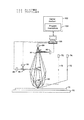
【選択図】図2
Description
本出願は、2006年2月9日に出願された米国仮出願60/772,418号「ウエハの特性決定のための方法とシステム」への優先権を請求するものであり、該仮出願はここに詳述された参照文献として取り扱われる。
Claims (22)
- ウエハの特性を決定するための方法であって、当該方法は、
出力が、ウエハ上の欠陥に対応する第一出力と、欠陥に対応しない第二出力を含む条件下で、検査システムを用い、ウエハからの光に対応する出力を生成することと、
前記第一出力ではなく前記第二出力を用いて、ウエハの特性の値を決定すること、
を含み、
前記第一出力と前記第二出力は同一の検知器により生成され、
前記決定することが、第二出力と前記特性の間の予め定められた相関を用い、前記特性の値を決定することを含み、前記特性は、計測学ツールを用いて測定可能なウエハの非欠陥関連特性であり、前記特性はウェハの物理的量である
ことを特徴とするウエハの特性を決定するための方法。 - ウエハからの光が拡散散乱光を含むことを特徴とする請求項1に記載の方法。
- 生成することが、レーザーにより生成された光によりウエハを照らすことを特徴とする請求項1に記載の方法。
- 生成することが、ウエハに亘り光を走査し、ウエハに亘り出力を生成することを特徴とする請求項1に記載の方法。
- 生成することが、ウエハの実質的全表面に亘り出力を生成することを特徴とする請求項1に記載の方法。
- 生成することが、ウエハの実質的全表面に亘り出力を生成することを特徴とし、そして、決定することが、ウエハの実質的全表面に亘り生成された第二出力を用い、前記特性の値を決定することを特徴とする請求項1に記載の方法。
- 決定することが、ウエハ上の領域に亘り第二出力の値を決定し、該値からの前記特性の値を決定することを特徴とする請求項1に記載の方法。
- 前記特性が、ウエハ上の領域に亘る特性の平均値であることを特徴とする請求項1に記載の方法。
- 決定することが、ウエハに亘る第二出力の変動を決定し、該変動から前記特性の値を決定することを特徴とする請求項1に記載の方法。
- 決定することが、ウエハの実質的全表面に亘り第二出力の二次元マップを生成し、該二次元マップよりウエハの前記特性の値を決定することを特徴とする請求項1に記載の方法。
- 決定することが、ウエハ上の異なる領域に亘る第二出力に関する値を決定し、そして該値を用い、異なる領域に関する前記特性の値を決定することを特徴とする請求項1に記載の方法。
- 決定することが、ウエハ上の異なる領域に関する特性の単一の値を決定し、そして異なる領域のそれぞれは、ウエハ上のパターン化された特徴の領域よりも大きいことを特徴とする請求項1に記載の方法。
- 生成することが、検査システムのマルチ・チャネルを用いて出力を生成することを特徴とし、決定することが、マルチ・チャネルの内の一つのチャネルにより生成された第二出力を用いて、特性を決定することを特徴とし、そして更に方法が、マルチ・チャネルの内の別の一つのチャネルより第二出力を用いて、ウエハの異なる特性を決定することを特徴とする請求項1に記載の方法。
- 更に、特性を用いて、統計的工程管理を実施することを特徴とする請求項1に記載の方法。
- 更に、半導体製造工程内のエクスカーションを検知するための特性を用い、半導体製造工程のインライン監視を実施することを特徴とする請求項1に記載の方法。
- 更に、ウエハ上の異なる領域に関する第二出力の標準偏差を決定し、該標準偏差が、ウエハ形成に用いられたプロセス内のエクスカーションを示すかを決定することを特徴とする請求項1に記載の方法。
- 更に、ウエハに亘り第二出力の変動を決定することと、ウエハの形成に使用されたプロセス・ツールの特徴に該変動が関連しているかを決定することを特徴とする請求項1に記載の方法。
- 更に、ウエハの実質的全表面に亘り第二出力の二次元マップを生成すること、二次元マップ内に異常なパターンが存在するかを決定すること、そして、異常なパターンが存在する場合、該異常パターンが、ウエハの形成に用いられたプロセス内のエクスカーションに対応するかを決定することを特徴とする請求項1に記載の方法。
- ウエハが、パターン化されてない、又はパターン化されたウエハを含むことを特徴とする請求項1に記載の方法。
- 更に、出力を用いウエハ上の欠陥を検知することを特徴とする請求項1に記載の方法。
- ウエハの特性を決定するためのコンピュータ実施方法であって、当該方法は、
出力が、ウエハ上の欠陥に対応する第一出力と、欠陥に対応しない第二出力を含む条件下で、検査システムにより生成されたウエハからの光に対応する出力を取得することと、
前記第一出力ではなく前記第二出力を用い、ウエハの特性の値を決定すること、
を含み、
前記第一出力と前記第二出力は同一の検知器により生成され、
前記決定することが、第二出力と前記特性の間の予め定められた相関を用い、前記特性の値を決定することを含み、前記特性は、計測学ツールを用いて測定可能なウエハの非欠陥関連特性であり、前記特性はウェハの物理的量である
ことを特徴とするウエハの特性を決定するためのコンピュータ実施方法。 - ウエハの特性を決定するためのシステムであって、当該システムは、
出力が、ウエハ上の欠陥に対応する第一出力と、欠陥に対応しない第二出力を含む条件下で、ウエハに光を当て、ウエハからの光に対応する出力を生成するように設定された検査サブシステムと、
前記第一出力ではなく前記第二出力を用い、ウエハの特性を決定するように設定されたプロセッサと、
を備え、
前記第一出力と前記第二出力は前記検査サブシステムの同一の検知器により生成され、
前記特性の値は、第二出力と前記特性の間の予め定められた相関を用いて決定され、
前記特性は、計測学ツールを用いて測定可能なウエハの非欠陥関連特性であり、前記特性はウェハの物理的量である
ことを特徴とするウエハの特性を決定するためのシステム。
Applications Claiming Priority (2)
| Application Number | Priority Date | Filing Date | Title |
|---|---|---|---|
| US77241806P | 2006-02-09 | 2006-02-09 | |
| US60/772,418 | 2006-02-09 |
Related Parent Applications (1)
| Application Number | Title | Priority Date | Filing Date |
|---|---|---|---|
| JP2008554517A Division JP2009526240A (ja) | 2006-02-09 | 2007-02-09 | ウエハの特性決定のための方法とシステム |
Related Child Applications (1)
| Application Number | Title | Priority Date | Filing Date |
|---|---|---|---|
| JP2014233048A Division JP6182737B2 (ja) | 2006-02-09 | 2014-11-17 | ウエハの特性決定のための方法とシステム |
Publications (2)
| Publication Number | Publication Date |
|---|---|
| JP2012198217A true JP2012198217A (ja) | 2012-10-18 |
| JP5718849B2 JP5718849B2 (ja) | 2015-05-13 |
Family
ID=38345969
Family Applications (3)
| Application Number | Title | Priority Date | Filing Date |
|---|---|---|---|
| JP2008554517A Pending JP2009526240A (ja) | 2006-02-09 | 2007-02-09 | ウエハの特性決定のための方法とシステム |
| JP2012094940A Active JP5718849B2 (ja) | 2006-02-09 | 2012-04-18 | ウエハの特性決定のための方法とシステム |
| JP2014233048A Active JP6182737B2 (ja) | 2006-02-09 | 2014-11-17 | ウエハの特性決定のための方法とシステム |
Family Applications Before (1)
| Application Number | Title | Priority Date | Filing Date |
|---|---|---|---|
| JP2008554517A Pending JP2009526240A (ja) | 2006-02-09 | 2007-02-09 | ウエハの特性決定のための方法とシステム |
Family Applications After (1)
| Application Number | Title | Priority Date | Filing Date |
|---|---|---|---|
| JP2014233048A Active JP6182737B2 (ja) | 2006-02-09 | 2014-11-17 | ウエハの特性決定のための方法とシステム |
Country Status (6)
| Country | Link |
|---|---|
| US (2) | US8284394B2 (ja) |
| EP (1) | EP1982160A4 (ja) |
| JP (3) | JP2009526240A (ja) |
| KR (1) | KR101324419B1 (ja) |
| SG (1) | SG170805A1 (ja) |
| WO (1) | WO2007092950A2 (ja) |
Families Citing this family (64)
| Publication number | Priority date | Publication date | Assignee | Title |
|---|---|---|---|---|
| US9188974B1 (en) | 2004-02-13 | 2015-11-17 | Kla-Tencor Technologies Corp. | Methods for improved monitor and control of lithography processes |
| US7676077B2 (en) | 2005-11-18 | 2010-03-09 | Kla-Tencor Technologies Corp. | Methods and systems for utilizing design data in combination with inspection data |
| US7570796B2 (en) | 2005-11-18 | 2009-08-04 | Kla-Tencor Technologies Corp. | Methods and systems for utilizing design data in combination with inspection data |
| WO2007137261A2 (en) * | 2006-05-22 | 2007-11-29 | Kla-Tencor Technologies Corporation | Methods and systems for detecting pinholes in a film formed on a wafer or for monitoring a thermal process tool |
| WO2008001922A1 (en) * | 2006-06-27 | 2008-01-03 | Nec Corporation | Method for analyzing warp of board or electronic component, system for analyzing warp of board or electronic component and program for analyzing warp of board or electronic component |
| US7650200B2 (en) * | 2007-03-30 | 2010-01-19 | Tokyo Electron Limited | Method and apparatus for creating a site-dependent evaluation library |
| US7596423B2 (en) * | 2007-03-30 | 2009-09-29 | Tokyo Electron Limited | Method and apparatus for verifying a site-dependent procedure |
| US7962863B2 (en) | 2007-05-07 | 2011-06-14 | Kla-Tencor Corp. | Computer-implemented methods, systems, and computer-readable media for determining a model for predicting printability of reticle features on a wafer |
| US7738093B2 (en) | 2007-05-07 | 2010-06-15 | Kla-Tencor Corp. | Methods for detecting and classifying defects on a reticle |
| US8213704B2 (en) * | 2007-05-09 | 2012-07-03 | Kla-Tencor Corp. | Methods and systems for detecting defects in a reticle design pattern |
| US7796804B2 (en) | 2007-07-20 | 2010-09-14 | Kla-Tencor Corp. | Methods for generating a standard reference die for use in a die to standard reference die inspection and methods for inspecting a wafer |
| US8611639B2 (en) * | 2007-07-30 | 2013-12-17 | Kla-Tencor Technologies Corp | Semiconductor device property extraction, generation, visualization, and monitoring methods |
| TWI469235B (zh) * | 2007-08-20 | 2015-01-11 | Kla Tencor Corp | 決定實際缺陷是潛在系統性缺陷或潛在隨機缺陷之由電腦實施之方法 |
| US8126255B2 (en) | 2007-09-20 | 2012-02-28 | Kla-Tencor Corp. | Systems and methods for creating persistent data for a wafer and for using persistent data for inspection-related functions |
| JP4898713B2 (ja) * | 2008-01-17 | 2012-03-21 | 株式会社日立ハイテクノロジーズ | 表面検査装置および表面検査方法 |
| US7912658B2 (en) * | 2008-05-28 | 2011-03-22 | Kla-Tencor Corp. | Systems and methods for determining two or more characteristics of a wafer |
| KR101647010B1 (ko) * | 2008-06-19 | 2016-08-10 | 케이엘에이-텐코어 코오포레이션 | 웨이퍼의 하나 이상의 특성들을 결정하기 위한 컴퓨터-구현 방법들, 컴퓨터-판독 가능 매체, 및 시스템들 |
| US8269960B2 (en) * | 2008-07-24 | 2012-09-18 | Kla-Tencor Corp. | Computer-implemented methods for inspecting and/or classifying a wafer |
| KR101729669B1 (ko) | 2008-07-28 | 2017-04-24 | 케이엘에이-텐코어 코오포레이션 | 웨이퍼 상의 메모리 디바이스 영역에서 검출된 결함들을 분류하기 위한 컴퓨터-구현 방법들, 컴퓨터-판독 가능 매체, 및 시스템들 |
| US7623229B1 (en) | 2008-10-07 | 2009-11-24 | Kla-Tencor Corporation | Systems and methods for inspecting wafers |
| US8223327B2 (en) | 2009-01-26 | 2012-07-17 | Kla-Tencor Corp. | Systems and methods for detecting defects on a wafer |
| US8605275B2 (en) * | 2009-01-26 | 2013-12-10 | Kla-Tencor Corp. | Detecting defects on a wafer |
| US8775101B2 (en) | 2009-02-13 | 2014-07-08 | Kla-Tencor Corp. | Detecting defects on a wafer |
| US8204297B1 (en) | 2009-02-27 | 2012-06-19 | Kla-Tencor Corp. | Methods and systems for classifying defects detected on a reticle |
| US8112241B2 (en) * | 2009-03-13 | 2012-02-07 | Kla-Tencor Corp. | Methods and systems for generating an inspection process for a wafer |
| US10324046B1 (en) * | 2009-06-03 | 2019-06-18 | Kla-Tencor Corp. | Methods and systems for monitoring a non-defect related characteristic of a patterned wafer |
| JP5557482B2 (ja) * | 2009-06-23 | 2014-07-23 | 株式会社日立製作所 | 検査性評価方法 |
| US8781781B2 (en) | 2010-07-30 | 2014-07-15 | Kla-Tencor Corp. | Dynamic care areas |
| US9170211B2 (en) | 2011-03-25 | 2015-10-27 | Kla-Tencor Corp. | Design-based inspection using repeating structures |
| US9087367B2 (en) | 2011-09-13 | 2015-07-21 | Kla-Tencor Corp. | Determining design coordinates for wafer defects |
| KR101906647B1 (ko) * | 2011-09-27 | 2018-10-10 | 케이엘에이-텐코 코포레이션 | 고처리량 박막 특성화 및 결함 검출 |
| US8982362B2 (en) | 2011-10-04 | 2015-03-17 | First Solar, Inc. | System and method for measuring layer thickness and depositing semiconductor layers |
| NL2009853A (en) | 2011-12-23 | 2013-06-26 | Asml Netherlands Bv | Methods and apparatus for measuring a property of a substrate. |
| US9665931B2 (en) | 2011-12-28 | 2017-05-30 | Sunedison Semiconductor Limited (Uen201334164H) | Air pocket detection methods and systems |
| CN103186053A (zh) * | 2011-12-30 | 2013-07-03 | 无锡华润上华科技有限公司 | 一种光刻条件控制方法 |
| US8831334B2 (en) | 2012-01-20 | 2014-09-09 | Kla-Tencor Corp. | Segmentation for wafer inspection |
| US8826200B2 (en) | 2012-05-25 | 2014-09-02 | Kla-Tencor Corp. | Alteration for wafer inspection |
| US9189844B2 (en) | 2012-10-15 | 2015-11-17 | Kla-Tencor Corp. | Detecting defects on a wafer using defect-specific information |
| US8912495B2 (en) * | 2012-11-21 | 2014-12-16 | Kla-Tencor Corp. | Multi-spectral defect inspection for 3D wafers |
| US9053527B2 (en) | 2013-01-02 | 2015-06-09 | Kla-Tencor Corp. | Detecting defects on a wafer |
| US9134254B2 (en) | 2013-01-07 | 2015-09-15 | Kla-Tencor Corp. | Determining a position of inspection system output in design data space |
| US9311698B2 (en) | 2013-01-09 | 2016-04-12 | Kla-Tencor Corp. | Detecting defects on a wafer using template image matching |
| US9092846B2 (en) | 2013-02-01 | 2015-07-28 | Kla-Tencor Corp. | Detecting defects on a wafer using defect-specific and multi-channel information |
| US9222895B2 (en) | 2013-02-25 | 2015-12-29 | Kla-Tencor Corp. | Generalized virtual inspector |
| US9008410B2 (en) | 2013-03-13 | 2015-04-14 | Kla-Tencor Corporation | Single die inspection on a dark field inspection tool |
| JP6046535B2 (ja) * | 2013-03-27 | 2016-12-14 | 株式会社東京精密 | 半導体ウエハマッピング方法及び半導体ウエハのレーザ加工方法 |
| US9865512B2 (en) | 2013-04-08 | 2018-01-09 | Kla-Tencor Corp. | Dynamic design attributes for wafer inspection |
| US9310320B2 (en) | 2013-04-15 | 2016-04-12 | Kla-Tencor Corp. | Based sampling and binning for yield critical defects |
| US9183624B2 (en) | 2013-06-19 | 2015-11-10 | Kla-Tencor Corp. | Detecting defects on a wafer with run time use of design data |
| US10290088B2 (en) * | 2014-02-14 | 2019-05-14 | Kla-Tencor Corporation | Wafer and lot based hierarchical method combining customized metrics with a global classification methodology to monitor process tool condition at extremely high throughput |
| US9816939B2 (en) | 2014-07-22 | 2017-11-14 | Kla-Tencor Corp. | Virtual inspection systems with multiple modes |
| WO2016196216A1 (en) * | 2015-05-29 | 2016-12-08 | Sunedison Semiconductor Limited | Methods for processing semiconductor wafers having a polycrystalline finish |
| DE102016202239B3 (de) * | 2016-02-15 | 2017-07-20 | Globalfoundries Inc. | Schneller Aufheizprozess bei der Herstellung von Halbleiterbauelementen |
| US10563973B2 (en) | 2016-03-28 | 2020-02-18 | Kla-Tencor Corporation | All surface film metrology system |
| CN106363468B (zh) * | 2016-12-02 | 2018-06-08 | 苏州辛德斯机器人系统工程有限公司 | 机械抛光过程的建模仿真方法及装置 |
| US11237872B2 (en) | 2017-05-23 | 2022-02-01 | Kla-Tencor Corporation | Semiconductor inspection and metrology systems for distributing job among the CPUs or GPUs based on logical image processing boundaries |
| US10585049B2 (en) | 2018-03-10 | 2020-03-10 | Kla-Tencor Corporation | Process-induced excursion characterization |
| US10359706B1 (en) * | 2018-06-11 | 2019-07-23 | Kla-Tencor Corporation | Integrated scanning electron microscopy and optical analysis techniques for advanced process control |
| US10949964B2 (en) | 2018-09-21 | 2021-03-16 | Kla Corporation | Super-resolution defect review image generation through generative adversarial networks |
| CN109738447B (zh) * | 2018-12-14 | 2021-12-21 | 惠州锂威新能源科技有限公司 | 一种电池极片保护胶的自动纠偏方法及装置 |
| US11561481B2 (en) | 2020-07-20 | 2023-01-24 | International Business Machines Corporation | Using E0 exposures for track/cluster monitoring |
| WO2023151286A1 (zh) * | 2022-02-14 | 2023-08-17 | 四川大学华西医院 | 不同设备检测同一指标同质化换算方法、装置、电子设备 |
| CN114166768B (zh) * | 2022-02-14 | 2022-05-20 | 四川大学华西医院 | 不同设备检测同一指标同质化换算方法、装置、电子设备 |
| KR20240127122A (ko) | 2023-02-15 | 2024-08-22 | 삼성전자주식회사 | 결함 검사 장치 및 결함 검사 방법 |
Citations (4)
| Publication number | Priority date | Publication date | Assignee | Title |
|---|---|---|---|---|
| JPH11237226A (ja) * | 1997-11-28 | 1999-08-31 | Hitachi Ltd | 欠陥検査装置 |
| JP2004524538A (ja) * | 2001-04-06 | 2004-08-12 | ケーエルエー−テンカー コーポレイション | 不良検出システムの改良 |
| WO2004105087A2 (en) * | 2003-05-19 | 2004-12-02 | Kla-Tencor Technologies Corporation | Apparatus and methods for enabling robust separation between signals of interest and noise |
| WO2005090650A1 (ja) * | 2004-03-19 | 2005-09-29 | Nippon Mining & Metals Co., Ltd. | 化合物半導体基板 |
Family Cites Families (103)
| Publication number | Priority date | Publication date | Assignee | Title |
|---|---|---|---|---|
| US4162126A (en) * | 1976-12-10 | 1979-07-24 | Hitachi, Ltd. | Surface detect test apparatus |
| DE3027373A1 (de) * | 1979-07-20 | 1981-03-19 | Hitachi, Ltd., Tokyo | Verfahren und einrichtung zur oberflaechenpruefung |
| US4898471A (en) | 1987-06-18 | 1990-02-06 | Tencor Instruments | Particle detection on patterned wafers and the like |
| US4845558A (en) | 1987-12-03 | 1989-07-04 | Kla Instruments Corporation | Method and apparatus for detecting defects in repeated microminiature patterns |
| JP2849627B2 (ja) * | 1989-02-27 | 1999-01-20 | 富士ゼロックス株式会社 | 画像処理装置 |
| US5027122A (en) * | 1990-03-12 | 1991-06-25 | Raytheon Company | Method and apparatus for doppler velocity de-aliasing |
| JPH06244261A (ja) * | 1990-12-31 | 1994-09-02 | Texas Instr Inc <Ti> | 半導体装置製造プロセス制御用センサ |
| JP2760250B2 (ja) | 1993-02-03 | 1998-05-28 | 株式会社デンソー | ピンホール検査装置 |
| US5355212A (en) * | 1993-07-19 | 1994-10-11 | Tencor Instruments | Process for inspecting patterned wafers |
| US5517234A (en) | 1993-10-26 | 1996-05-14 | Gerber Systems Corporation | Automatic optical inspection system having a weighted transition database |
| US6271916B1 (en) | 1994-03-24 | 2001-08-07 | Kla-Tencor Corporation | Process and assembly for non-destructive surface inspections |
| DE19526373B4 (de) * | 1994-08-08 | 2005-10-20 | Tokyo Kikai Seisakusho Ltd | Vorrichtung zur Registersteuerung bei Rollenrotationsdruckmaschinen und automatisches Verfahren zur Registersteuerung für Rollenrotationsdruckmaschinen zur Korrektur von Registereinstellfehlern |
| JP3055598B2 (ja) | 1994-09-16 | 2000-06-26 | 信越半導体株式会社 | シリコンウエーハの評価方法 |
| US5661408A (en) * | 1995-03-01 | 1997-08-26 | Qc Solutions, Inc. | Real-time in-line testing of semiconductor wafers |
| US6118525A (en) | 1995-03-06 | 2000-09-12 | Ade Optical Systems Corporation | Wafer inspection system for distinguishing pits and particles |
| US5712701A (en) | 1995-03-06 | 1998-01-27 | Ade Optical Systems Corporation | Surface inspection system and method of inspecting surface of workpiece |
| US5903342A (en) * | 1995-04-10 | 1999-05-11 | Hitachi Electronics Engineering, Co., Ltd. | Inspection method and device of wafer surface |
| US5991699A (en) | 1995-05-04 | 1999-11-23 | Kla Instruments Corporation | Detecting groups of defects in semiconductor feature space |
| US6507025B1 (en) * | 1995-10-23 | 2003-01-14 | Science Applications International Corporation | Density detection using real time discrete photon counting for fast moving targets |
| US5625451A (en) | 1995-11-27 | 1997-04-29 | Schmitt Measurement Systems, Inc. | Methods and apparatus for characterizing a surface |
| US6239868B1 (en) * | 1996-01-02 | 2001-05-29 | Lj Laboratories, L.L.C. | Apparatus and method for measuring optical characteristics of an object |
| US5877860A (en) | 1996-05-13 | 1999-03-02 | Boxer Cross, Inc. | System and method for measuring the microroughness of a surface of a substrate |
| AU6942998A (en) | 1997-03-31 | 1998-10-22 | Microtherm, Llc | Optical inspection module and method for detecting particles and defects on substrates in integrated process tools |
| JP3211872B2 (ja) * | 1997-07-29 | 2001-09-25 | 日本電気株式会社 | 薬液処理方法、半導体基板の処理方法及び半導体装置の製造方法 |
| US6201601B1 (en) | 1997-09-19 | 2001-03-13 | Kla-Tencor Corporation | Sample inspection system |
| JPH11132975A (ja) | 1997-10-31 | 1999-05-21 | Toshiba Corp | 電子ビームを用いた検査方法及びその装置 |
| US6157444A (en) | 1997-11-28 | 2000-12-05 | Hitachi, Ltd. | Defect inspection apparatus for silicon wafer |
| JPH11243041A (ja) | 1998-02-26 | 1999-09-07 | Mitsubishi Electric Corp | 品質管理システムおよび記録媒体 |
| KR19990073971A (ko) | 1998-03-05 | 1999-10-05 | 윤종용 | 레이저를 이용한 다목적 측정설비 |
| TW389973B (en) * | 1998-03-12 | 2000-05-11 | United Microelectronics Corp | Method for inspecting wafer defects |
| JP2000002514A (ja) | 1998-06-17 | 2000-01-07 | Nikon Corp | 膜厚測定装置及びアライメントセンサ並びにアライメント装置 |
| US6603877B1 (en) | 1999-06-01 | 2003-08-05 | Beltronics, Inc. | Method of and apparatus for optical imaging inspection of multi-material objects and the like |
| KR20010001224A (ko) | 1999-06-02 | 2001-01-05 | 윤종용 | 웨이퍼 불량검사 방법 및 장치 |
| US6342704B1 (en) * | 1999-08-04 | 2002-01-29 | Taiwan Semiconductor Manufacturing Company, Ltd | Method and apparatus for detecting nitride residue on semiconductor wafers |
| US6440612B1 (en) * | 1999-09-01 | 2002-08-27 | Micron Technology, Inc. | Field correction of overlay error |
| JP3987246B2 (ja) * | 1999-09-17 | 2007-10-03 | 株式会社東芝 | 露光用マスク及び半導体装置の製造方法 |
| US6552337B1 (en) * | 1999-11-02 | 2003-04-22 | Samsung Electronics Co., Ltd. | Methods and systems for measuring microroughness of a substrate combining particle counter and atomic force microscope measurements |
| JP2001163312A (ja) | 1999-12-03 | 2001-06-19 | Jiyooben Denki Kk | 密封包装物の検査方法及びその装置 |
| TW571089B (en) | 2000-04-21 | 2004-01-11 | Nikon Corp | Defect testing apparatus and defect testing method |
| US6590645B1 (en) | 2000-05-04 | 2003-07-08 | Kla-Tencor Corporation | System and methods for classifying anomalies of sample surfaces |
| US6919957B2 (en) * | 2000-09-20 | 2005-07-19 | Kla-Tencor Technologies Corp. | Methods and systems for determining a critical dimension, a presence of defects, and a thin film characteristic of a specimen |
| US6891627B1 (en) * | 2000-09-20 | 2005-05-10 | Kla-Tencor Technologies Corp. | Methods and systems for determining a critical dimension and overlay of a specimen |
| US6633831B2 (en) | 2000-09-20 | 2003-10-14 | Kla Tencor Technologies | Methods and systems for determining a critical dimension and a thin film characteristic of a specimen |
| US6673637B2 (en) | 2000-09-20 | 2004-01-06 | Kla-Tencor Technologies | Methods and systems for determining a presence of macro defects and overlay of a specimen |
| US6797975B2 (en) | 2000-09-21 | 2004-09-28 | Hitachi, Ltd. | Method and its apparatus for inspecting particles or defects of a semiconductor device |
| US6636031B1 (en) | 2000-10-05 | 2003-10-21 | Sanko Electronic Laboratory Co., Ltd. | Method and device for detecting pinholes in organic film on concrete surface |
| US6898305B2 (en) | 2001-02-22 | 2005-05-24 | Hitachi, Ltd. | Circuit pattern inspection method and apparatus |
| JP3596479B2 (ja) | 2001-03-05 | 2004-12-02 | 森 勇蔵 | 光散乱法による表面の複合評価システム |
| US6538730B2 (en) | 2001-04-06 | 2003-03-25 | Kla-Tencor Technologies Corporation | Defect detection system |
| JP3210654B1 (ja) | 2001-05-02 | 2001-09-17 | レーザーテック株式会社 | 光学式走査装置及び欠陥検出装置 |
| KR100515491B1 (ko) | 2001-12-07 | 2005-09-16 | 다이닛뽕스크린 세이조오 가부시키가이샤 | 반도체 기판 상의 패턴을 검사하는 장치와 방법 및 컴퓨터판독 가능한 기록매체 |
| US7369735B2 (en) | 2002-02-15 | 2008-05-06 | Biosynergetics, Inc. | Apparatus for the collection and transmission of electromagnetic radiation |
| JP2003240723A (ja) * | 2002-02-19 | 2003-08-27 | Mitsubishi Electric Corp | 欠陥検査方法及び欠陥検査装置 |
| JP2003240713A (ja) | 2002-02-21 | 2003-08-27 | Toyobo Co Ltd | 材質の判別装置 |
| JP4102081B2 (ja) * | 2002-02-28 | 2008-06-18 | 株式会社荏原製作所 | 研磨装置及び研磨面の異物検出方法 |
| US7155052B2 (en) | 2002-06-10 | 2006-12-26 | Tokyo Seimitsu (Israel) Ltd | Method for pattern inspection |
| US6596553B1 (en) | 2002-06-26 | 2003-07-22 | Advanced Micro Devices, Inc. | Method of pinhole decoration and detection |
| US7283164B2 (en) * | 2002-09-18 | 2007-10-16 | Micron Technology, Inc. | Method for detecting and correcting defective pixels in a digital image sensor |
| WO2004031753A1 (en) * | 2002-09-30 | 2004-04-15 | Applied Materials Israel, Ltd. | Inspection system with oblique viewing angle |
| US6781688B2 (en) * | 2002-10-02 | 2004-08-24 | Kla-Tencor Technologies Corporation | Process for identifying defects in a substrate having non-uniform surface properties |
| JP4172761B2 (ja) | 2002-10-08 | 2008-10-29 | 大日本スクリーン製造株式会社 | 欠陥検査装置、欠陥検査方法およびプログラム |
| KR100492158B1 (ko) | 2002-11-19 | 2005-06-02 | 삼성전자주식회사 | 웨이퍼 검사 장치 |
| US7369233B2 (en) | 2002-11-26 | 2008-05-06 | Kla-Tencor Technologies Corporation | Optical system for measuring samples using short wavelength radiation |
| US6718526B1 (en) | 2003-02-07 | 2004-04-06 | Kla-Tencor Corporation | Spatial signature analysis |
| WO2004111618A2 (en) | 2003-06-10 | 2004-12-23 | Ade Corporation | Method and system for classifiying defects occurring at a surface of a substrate using graphical representation of multi-channel data |
| US6952265B2 (en) * | 2003-06-12 | 2005-10-04 | E. I. Du Pont De Nemours And Company | Method of characterization of surface coating containing metallic flakes and device used therein |
| JP4117556B2 (ja) * | 2003-09-08 | 2008-07-16 | ノーリツ鋼機株式会社 | フィルム画像処理装置及びフィルム画像処理方法 |
| US7110106B2 (en) | 2003-10-29 | 2006-09-19 | Coretech Optical, Inc. | Surface inspection system |
| US7006886B1 (en) | 2004-01-12 | 2006-02-28 | Kla Tencor-Technologies Corporation | Detection of spatially repeating signatures |
| US7315642B2 (en) | 2004-02-12 | 2008-01-01 | Applied Materials, Israel, Ltd. | System and method for measuring thin film thickness variations and for compensating for the variations |
| KR100590542B1 (ko) | 2004-02-21 | 2006-06-19 | 삼성전자주식회사 | Dna 칩의 오류 스팟 검출 방법 및 그 시스템 |
| US7373277B1 (en) | 2004-03-09 | 2008-05-13 | Kla-Tencor Technologies Corp. | Methods and systems for detection of selected defects particularly in relatively noisy inspection data |
| US7349079B2 (en) | 2004-05-14 | 2008-03-25 | Kla-Tencor Technologies Corp. | Methods for measurement or analysis of a nitrogen concentration of a specimen |
| US7359052B2 (en) | 2004-05-14 | 2008-04-15 | Kla-Tencor Technologies Corp. | Systems and methods for measurement of a specimen with vacuum ultraviolet light |
| US7564552B2 (en) | 2004-05-14 | 2009-07-21 | Kla-Tencor Technologies Corp. | Systems and methods for measurement of a specimen with vacuum ultraviolet light |
| US7067819B2 (en) | 2004-05-14 | 2006-06-27 | Kla-Tencor Technologies Corp. | Systems and methods for measurement or analysis of a specimen using separated spectral peaks in light |
| JP2006038779A (ja) | 2004-07-30 | 2006-02-09 | Hitachi High-Technologies Corp | パターン形状評価方法、評価装置、及び半導体装置の製造方法 |
| JP4904034B2 (ja) | 2004-09-14 | 2012-03-28 | ケーエルエー−テンカー コーポレイション | レチクル・レイアウト・データを評価するための方法、システム及び搬送媒体 |
| US20060192950A1 (en) | 2004-12-19 | 2006-08-31 | Neil Judell | System and method for inspecting a workpiece surface using combinations of light collectors |
| WO2006116386A1 (en) * | 2005-04-25 | 2006-11-02 | X-Rite, Incorporated | Measuring an appearance property of a surface using a spatially under-sampled bidirectional reflectance distribution function |
| JP4988223B2 (ja) | 2005-06-22 | 2012-08-01 | 株式会社日立ハイテクノロジーズ | 欠陥検査装置およびその方法 |
| US7570796B2 (en) | 2005-11-18 | 2009-08-04 | Kla-Tencor Technologies Corp. | Methods and systems for utilizing design data in combination with inspection data |
| US7676077B2 (en) | 2005-11-18 | 2010-03-09 | Kla-Tencor Technologies Corp. | Methods and systems for utilizing design data in combination with inspection data |
| KR100738809B1 (ko) | 2006-02-01 | 2007-07-12 | 동부일렉트로닉스 주식회사 | 웨이퍼 표면 검사 시스템 및 그 제어방법 |
| WO2007137261A2 (en) | 2006-05-22 | 2007-11-29 | Kla-Tencor Technologies Corporation | Methods and systems for detecting pinholes in a film formed on a wafer or for monitoring a thermal process tool |
| JP2008004641A (ja) | 2006-06-20 | 2008-01-10 | Toshiba Corp | 不良検出システム、不良検出方法及びプログラム |
| JP2008039743A (ja) | 2006-08-10 | 2008-02-21 | Tokyo Seimitsu Co Ltd | 外観検査装置及び外観検査方法 |
| JP5221858B2 (ja) | 2006-08-30 | 2013-06-26 | 株式会社日立ハイテクノロジーズ | 欠陥検査装置、及び欠陥検査方法 |
| JP2008096430A (ja) | 2006-09-13 | 2008-04-24 | Hitachi High-Technologies Corp | 欠陥検査方法およびその装置 |
| US7728969B2 (en) | 2006-12-05 | 2010-06-01 | Kla-Tencor Technologies Corp. | Methods and systems for identifying defect types on a wafer |
| US7904845B2 (en) | 2006-12-06 | 2011-03-08 | Kla-Tencor Corp. | Determining locations on a wafer to be reviewed during defect review |
| WO2008077100A2 (en) | 2006-12-19 | 2008-06-26 | Kla-Tencor Corporation | Systems and methods for creating inspection recipes |
| WO2008086282A2 (en) | 2007-01-05 | 2008-07-17 | Kla-Tencor Corporation | Methods and systems for using electrical information for a device being fabricated on a wafer to perform one or more defect-related functions |
| US7894659B2 (en) | 2007-02-28 | 2011-02-22 | Kla-Tencor Technologies Corp. | Methods for accurate identification of an edge of a care area for an array area formed on a wafer and methods for binning defects detected in an array area formed on a wafer |
| US7925072B2 (en) | 2007-03-08 | 2011-04-12 | Kla-Tencor Technologies Corp. | Methods for identifying array areas in dies formed on a wafer and methods for setting up such methods |
| US8611639B2 (en) | 2007-07-30 | 2013-12-17 | Kla-Tencor Technologies Corp | Semiconductor device property extraction, generation, visualization, and monitoring methods |
| US20110304527A1 (en) | 2007-09-14 | 2011-12-15 | Sean Wu | Computer-implemented methods, carrier media, and systems for displaying an image of at least a portion of a wafer |
| US8126255B2 (en) | 2007-09-20 | 2012-02-28 | Kla-Tencor Corp. | Systems and methods for creating persistent data for a wafer and for using persistent data for inspection-related functions |
| JP5159373B2 (ja) | 2008-03-06 | 2013-03-06 | オリンパス株式会社 | 基板検査方法 |
| US7589845B1 (en) | 2008-03-27 | 2009-09-15 | Tokyo Electron Limited | Process control using an optical metrology system optimized with signal criteria |
| US7912658B2 (en) * | 2008-05-28 | 2011-03-22 | Kla-Tencor Corp. | Systems and methods for determining two or more characteristics of a wafer |
| KR101647010B1 (ko) | 2008-06-19 | 2016-08-10 | 케이엘에이-텐코어 코오포레이션 | 웨이퍼의 하나 이상의 특성들을 결정하기 위한 컴퓨터-구현 방법들, 컴퓨터-판독 가능 매체, 및 시스템들 |
| US8269960B2 (en) | 2008-07-24 | 2012-09-18 | Kla-Tencor Corp. | Computer-implemented methods for inspecting and/or classifying a wafer |
-
2007
- 2007-02-09 JP JP2008554517A patent/JP2009526240A/ja active Pending
- 2007-02-09 WO PCT/US2007/061912 patent/WO2007092950A2/en not_active Ceased
- 2007-02-09 EP EP07763569.6A patent/EP1982160A4/en not_active Withdrawn
- 2007-02-09 US US11/673,150 patent/US8284394B2/en active Active
- 2007-02-09 KR KR1020087022070A patent/KR101324419B1/ko active Active
- 2007-02-09 SG SG201102259-7A patent/SG170805A1/en unknown
-
2012
- 2012-04-18 JP JP2012094940A patent/JP5718849B2/ja active Active
- 2012-09-12 US US13/610,860 patent/US8422010B2/en active Active
-
2014
- 2014-11-17 JP JP2014233048A patent/JP6182737B2/ja active Active
Patent Citations (5)
| Publication number | Priority date | Publication date | Assignee | Title |
|---|---|---|---|---|
| JPH11237226A (ja) * | 1997-11-28 | 1999-08-31 | Hitachi Ltd | 欠陥検査装置 |
| JP2004524538A (ja) * | 2001-04-06 | 2004-08-12 | ケーエルエー−テンカー コーポレイション | 不良検出システムの改良 |
| WO2004105087A2 (en) * | 2003-05-19 | 2004-12-02 | Kla-Tencor Technologies Corporation | Apparatus and methods for enabling robust separation between signals of interest and noise |
| JP2007501944A (ja) * | 2003-05-19 | 2007-02-01 | ケーエルエー−テンカー テクノロジィース コーポレイション | 対象となる信号およびノイズ間のロバストな分離を可能にする装置および方法 |
| WO2005090650A1 (ja) * | 2004-03-19 | 2005-09-29 | Nippon Mining & Metals Co., Ltd. | 化合物半導体基板 |
Also Published As
| Publication number | Publication date |
|---|---|
| KR20080100363A (ko) | 2008-11-17 |
| US20080013083A1 (en) | 2008-01-17 |
| US8422010B2 (en) | 2013-04-16 |
| JP6182737B2 (ja) | 2017-08-23 |
| SG170805A1 (en) | 2011-05-30 |
| US8284394B2 (en) | 2012-10-09 |
| KR101324419B1 (ko) | 2013-11-01 |
| JP2009526240A (ja) | 2009-07-16 |
| WO2007092950A2 (en) | 2007-08-16 |
| US20130035877A1 (en) | 2013-02-07 |
| JP5718849B2 (ja) | 2015-05-13 |
| JP2015099148A (ja) | 2015-05-28 |
| EP1982160A4 (en) | 2016-02-17 |
| WO2007092950A3 (en) | 2008-04-17 |
| EP1982160A2 (en) | 2008-10-22 |
Similar Documents
| Publication | Publication Date | Title |
|---|---|---|
| JP6182737B2 (ja) | ウエハの特性決定のための方法とシステム | |
| US7528944B2 (en) | Methods and systems for detecting pinholes in a film formed on a wafer or for monitoring a thermal process tool | |
| KR101506894B1 (ko) | 웨이퍼의 두 개 또는 그 초과의 특성들을 결정하기 위한 시스템들 및 방법들 | |
| US8411264B2 (en) | Method and apparatus for inspecting defects | |
| US7747062B2 (en) | Methods, defect review tools, and systems for locating a defect in a defect review process | |
| JP3566589B2 (ja) | 欠陥検査装置およびその方法 | |
| JP6545164B2 (ja) | ウェハ検査プロセスの1つ以上のパラメータを決定するための方法、コンピュータ読み出し可能な媒体およびシステム | |
| US7271921B2 (en) | Method and apparatus for determining surface layer thickness using continuous multi-wavelength surface scanning | |
| US8755045B2 (en) | Detecting method for forming semiconductor device | |
| US5801824A (en) | Large area defect monitor tool for manufacture of clean surfaces | |
| US5631733A (en) | Large area defect monitor tool for manufacture of clean surfaces | |
| JP2004301847A (ja) | 欠陥検査装置およびその方法 | |
| Yang | Metrology and Inspection Equipment | |
| TWI870091B (zh) | 老化條件的評估裝置及設定方法 |
Legal Events
| Date | Code | Title | Description |
|---|---|---|---|
| A131 | Notification of reasons for refusal |
Free format text: JAPANESE INTERMEDIATE CODE: A131 Effective date: 20131008 |
|
| A601 | Written request for extension of time |
Free format text: JAPANESE INTERMEDIATE CODE: A601 Effective date: 20140108 |
|
| A602 | Written permission of extension of time |
Free format text: JAPANESE INTERMEDIATE CODE: A602 Effective date: 20140114 |
|
| A601 | Written request for extension of time |
Free format text: JAPANESE INTERMEDIATE CODE: A601 Effective date: 20140210 |
|
| A602 | Written permission of extension of time |
Free format text: JAPANESE INTERMEDIATE CODE: A602 Effective date: 20140214 |
|
| A601 | Written request for extension of time |
Free format text: JAPANESE INTERMEDIATE CODE: A601 Effective date: 20140310 |
|
| A602 | Written permission of extension of time |
Free format text: JAPANESE INTERMEDIATE CODE: A602 Effective date: 20140313 |
|
| A02 | Decision of refusal |
Free format text: JAPANESE INTERMEDIATE CODE: A02 Effective date: 20140715 |
|
| A521 | Request for written amendment filed |
Free format text: JAPANESE INTERMEDIATE CODE: A523 Effective date: 20141117 |
|
| A911 | Transfer to examiner for re-examination before appeal (zenchi) |
Free format text: JAPANESE INTERMEDIATE CODE: A911 Effective date: 20141216 |
|
| TRDD | Decision of grant or rejection written | ||
| A01 | Written decision to grant a patent or to grant a registration (utility model) |
Free format text: JAPANESE INTERMEDIATE CODE: A01 Effective date: 20150317 |
|
| A61 | First payment of annual fees (during grant procedure) |
Free format text: JAPANESE INTERMEDIATE CODE: A61 Effective date: 20150319 |
|
| R150 | Certificate of patent or registration of utility model |
Ref document number: 5718849 Country of ref document: JP Free format text: JAPANESE INTERMEDIATE CODE: R150 |
|
| R250 | Receipt of annual fees |
Free format text: JAPANESE INTERMEDIATE CODE: R250 |
|
| R250 | Receipt of annual fees |
Free format text: JAPANESE INTERMEDIATE CODE: R250 |
|
| R250 | Receipt of annual fees |
Free format text: JAPANESE INTERMEDIATE CODE: R250 |
|
| R250 | Receipt of annual fees |
Free format text: JAPANESE INTERMEDIATE CODE: R250 |
|
| R250 | Receipt of annual fees |
Free format text: JAPANESE INTERMEDIATE CODE: R250 |
|
| R250 | Receipt of annual fees |
Free format text: JAPANESE INTERMEDIATE CODE: R250 |
|
| R250 | Receipt of annual fees |
Free format text: JAPANESE INTERMEDIATE CODE: R250 |
|
| R250 | Receipt of annual fees |
Free format text: JAPANESE INTERMEDIATE CODE: R250 |