JP2012198894A - Synchronous data processing system and method - Google Patents
Synchronous data processing system and method Download PDFInfo
- Publication number
- JP2012198894A JP2012198894A JP2012062441A JP2012062441A JP2012198894A JP 2012198894 A JP2012198894 A JP 2012198894A JP 2012062441 A JP2012062441 A JP 2012062441A JP 2012062441 A JP2012062441 A JP 2012062441A JP 2012198894 A JP2012198894 A JP 2012198894A
- Authority
- JP
- Japan
- Prior art keywords
- data
- memory
- memory module
- clock signal
- module
- Prior art date
- Legal status (The legal status is an assumption and is not a legal conclusion. Google has not performed a legal analysis and makes no representation as to the accuracy of the status listed.)
- Pending
Links
Images




Classifications
-
- G—PHYSICS
- G11—INFORMATION STORAGE
- G11C—STATIC STORES
- G11C7/00—Arrangements for writing information into, or reading information out from, a digital store
- G11C7/22—Read-write [R-W] timing or clocking circuits; Read-write [R-W] control signal generators or management
-
- G—PHYSICS
- G06—COMPUTING OR CALCULATING; COUNTING
- G06F—ELECTRIC DIGITAL DATA PROCESSING
- G06F13/00—Interconnection of, or transfer of information or other signals between, memories, input/output devices or central processing units
- G06F13/14—Handling requests for interconnection or transfer
- G06F13/16—Handling requests for interconnection or transfer for access to memory bus
- G06F13/1668—Details of memory controller
- G06F13/1689—Synchronisation and timing concerns
-
- G—PHYSICS
- G06—COMPUTING OR CALCULATING; COUNTING
- G06F—ELECTRIC DIGITAL DATA PROCESSING
- G06F1/00—Details not covered by groups G06F3/00 - G06F13/00 and G06F21/00
-
- G—PHYSICS
- G11—INFORMATION STORAGE
- G11C—STATIC STORES
- G11C7/00—Arrangements for writing information into, or reading information out from, a digital store
- G11C7/10—Input/output [I/O] data interface arrangements, e.g. I/O data control circuits, I/O data buffers
Landscapes
- Engineering & Computer Science (AREA)
- Theoretical Computer Science (AREA)
- Physics & Mathematics (AREA)
- General Engineering & Computer Science (AREA)
- General Physics & Mathematics (AREA)
- Synchronisation In Digital Transmission Systems (AREA)
- Memory System (AREA)
- Dram (AREA)
Abstract
【課題】伝搬遅延およびPVT条件の変化時に高信頼性のデータ転送を可能とするデータ処理システムを提供する。
【解決手段】同期データ処理システムはデータを格納するメモリモジュールと、メモリモジュールに接続されたメモリコントローラとを備える。メモリコントローラのクロックインバータは入力クロック信号を受信し反転クロック信号をメモリモジュールに提供する。反転クロック信号によってメモリモジュール到達前の第1の伝搬遅延がメモリクロック信号として与えられる。メモリモジュールに接続された書込データバッファは入力クロック信号に応答してメモリモジュールにデータを提供する。メモリモジュールに接続された非同期先入れ先出しバッファはメモリクロック信号をバッファにフィードバックすることによって生成されるフィードバック信号に応答してメモリモジュールからデータを読み取る。
【選択図】図3A data processing system capable of highly reliable data transfer when propagation delay and PVT conditions change is provided.
A synchronous data processing system includes a memory module for storing data, and a memory controller connected to the memory module. The clock inverter of the memory controller receives the input clock signal and provides an inverted clock signal to the memory module. The first propagation delay before reaching the memory module is given as the memory clock signal by the inverted clock signal. A write data buffer connected to the memory module provides data to the memory module in response to an input clock signal. An asynchronous first-in first-out buffer connected to the memory module reads data from the memory module in response to a feedback signal generated by feeding back a memory clock signal to the buffer.
[Selection] Figure 3
Description
本発明は、一般にデータ処理システムに関する。より詳細には、本発明は、同期データ処理システムにおける高信頼性のデータ転送に関する。 The present invention generally relates to data processing systems. More particularly, the present invention relates to reliable data transfer in synchronous data processing systems.
マイクロコンピュータなどのデータ処理システムの動作速度が近年上昇するにつれ、そうしたシステムの性能を向上させるべく、マイクロプロセッサなどの周辺装置およびシンクロナス・ダイナミック・ランダム・アクセス・メモリ(SDRAM)などのメモリデバイスの動作速度も上昇している。プロセッサおよび周辺装置を接続するバスの動作周波数も上昇している。しかしながら、周波数の上昇につれ、データ転送における伝搬遅延およびPVT(プロセス、電圧、および温度)変化の影響は大きくなる。 As the operating speed of data processing systems such as microcomputers has increased in recent years, peripheral devices such as microprocessors and memory devices such as synchronous dynamic random access memory (SDRAM) have been improved to improve the performance of such systems. The operating speed is also increasing. The operating frequency of the bus connecting the processor and peripheral devices is also increasing. However, as frequency increases, the effects of propagation delays and PVT (process, voltage, and temperature) changes in data transfer increase.
特許文献1には、データ処理システムにおけるクロック同期について記載されている。通常、同期データ処理システムでは、メモリコントローラなどの部品とメモリデバイスとの間で転送されるクロックとデータ信号との間には、位相差(またはスキュー)が存在する。このような位相スキューは、伝搬遅延や、PVT変動によってもたらされる。周波数の上昇につれ、位相スキューが増大することがあり、それによって、読取または書込動作時に誤ったデータサンプリングが生じ得る。
位相スキューを減少させる1つの方法は、データサンプリングを改良するために位相同期回路(フェーズ・ロック・ループ、すなわち、PLL)を採用することである。図1は、PLL回路12を有する従来のデータ処理システム10のブロック図である。データ処理システム10は、メモリコントローラ14およびメモリモジュール16を備える。このうち、メモリコントローラ14が、メモリコントローラ14とメモリモジュール16との間で転送されるクロックとデータ信号との間の位相スキューを補償するためのPLL回路12を備える。
One way to reduce phase skew is to employ a phase locked loop (phase locked loop or PLL) to improve data sampling. FIG. 1 is a block diagram of a conventional
動作時には、メモリコントローラ14は、クロック信号生成器(図示せず)から入力クロック信号(IP_CLK)18を受信する。この入力クロック信号18は、読取および書込データバッファ20,22に供給される。また、メモリコントローラ14は、メモリモジュール16に対するメモリクロック信号23を生成する。ここで、メモリコントローラ14とメモリモジュール16との間で送信されるデータ信号(IP_DATA,MEM_DATA)は、参照符号24,26によって概略的に表される。
In operation, the
示すように、メモリクロック信号(MEM_CLK)23は、メモリコントローラ14とメモリモジュール16との間で半分だけループして戻され(ループバック)、クロックイン信号(CLK_IN)またはループバック信号28がPLL回路12に供給されて、クロックアウト信号(CLK_OUT)30が生成される。このフィードバック機構によって、データサンプリングが改良される。こうして、メモリコントローラ14およびメモリモジュール16によって観測されるクロック信号は整合され、それによって、読取および書込動作時のデータ転送における1つの完全なサイクルが提供される。ループバック信号(CLK_IN)28を有するPLL回路12によってシステムのデータサンプリングが改良されるが、そうした改良は、メモリコントローラ14とメモリモジュール16との間の伝搬遅延が1クロックサイクル未満の場合にのみ機能するという点において制限されている。
As shown, the memory clock signal (MEM_CLK) 23 is looped back by half between the
図2は、図1のデータ処理システム10のデータ読取および書込サイクルのタイミング図である。示した実施形態では、メモリクロック信号およびループバック信号のサイクルは、参照符号50,52によって表される。メモリクロック信号およびループバック信号50,52の位相は整合されている。さらに、書込動作時にメモリコントローラ14によって発生されてメモリモジュール16によって受信されるデータ信号は、参照符号54,56によって表される。同様に、メモリモジュール16によって送信されてメモリコントローラ14によって読み取られるデータ信号は、参照符号58,60によってそれぞれ表される。
FIG. 2 is a timing diagram of data read and write cycles of the
書込サイクルでは、データ(IP_DATA)54はクロック信号52(CLK_INに位相整合されているIP_CLK)の立ち上がりエッジにおいて書込データバッファ22から発生され、メモリモジュール16によってMEM_DATA56として受信される。読取サイクルでは、MEM_DATA58はメモリクロック信号(MEM_CLK)50の立ち上がりエッジにおいてメモリモジュール72から発生され、メモリコントローラ14によってIP_DATA60として読み取られる。
In the write cycle, data (IP_DATA) 54 is generated from the
参照符号62,64によって示すように伝搬遅延が1クロックサイクル近傍またはそれ以上であるとき、PLL回路12が書込および読取サイクルにおける位相スキューを補償できないことが理解される。残念なことに、これによって誤ったデータサンプリングが生じる。
It will be appreciated that the
加えて、PLL回路は回路板上の有意な面積を占めるとともに、通常、所定の周波数帯域用に設計されているので、そうしたPLL回路の特性決定には時間が掛かり、上述のように、PVT条件が変化することによる影響を受けがちである。 In addition, since the PLL circuit occupies a significant area on the circuit board and is usually designed for a predetermined frequency band, it takes time to determine the characteristics of such a PLL circuit. Tend to be affected by changes in
したがって、伝搬遅延およびPVT条件が変化している場合に高信頼性のデータ転送を可能とするデータ処理システムの必要性が存在する。 Therefore, there is a need for a data processing system that enables reliable data transfer when propagation delays and PVT conditions are changing.
一実施形態では、本発明によって、同期データ処理システムを提供する。この同期データ処理システムは、データを格納するためのメモリモジュールと、該メモリモジュールに接続されているメモリコントローラとを備える。メモリコントローラは、入力クロック信号を受信し、反転クロック信号をメモリモジュールに提供するためのクロックインバータを備える。この反転クロック信号によって、メモリモジュールに到達する前の第1の伝搬遅延がメモリクロック信号として与えられる。メモリモジュールには、書込データバッファが接続されている。書込データバッファは、入力クロック信号に応答してメモリモジュールにデータを提供する。メモリモジュールには、非同期先入れ先出し(ASYNC FIFO)バッファが接続されている。このASYNC FIFOバッファは、メモリクロック信号をASYNC FIFOバッファにフィードバックすることによって生成されるフィードバック信号に応答して、メモリモジュールからデータを読み取る。 In one embodiment, the present invention provides a synchronous data processing system. The synchronous data processing system includes a memory module for storing data, and a memory controller connected to the memory module. The memory controller includes a clock inverter for receiving an input clock signal and providing an inverted clock signal to the memory module. By this inverted clock signal, the first propagation delay before reaching the memory module is given as the memory clock signal. A write data buffer is connected to the memory module. The write data buffer provides data to the memory module in response to the input clock signal. An asynchronous first-in first-out (ASYNC FIFO) buffer is connected to the memory module. The ASYNC FIFO buffer reads data from the memory module in response to a feedback signal generated by feeding back the memory clock signal to the ASYNC FIFO buffer.
別の実施形態では、本発明によって、同期データ処理システムにおいてメモリモジュールとメモリコントローラとの間でデータを転送する方法を提供する。この方法は、入力クロック信号を受信するステップと、メモリモジュールに対するメモリクロック信号を生成するべく、反転入力クロック信号をメモリモジュールに送信するステップとを備える。メモリクロック信号は、メモリモジュールからメモリコントローラにフィードバックされ、
メモリコントローラとメモリモジュールとの間で転送されるクロック信号によって、メモリモジュールとメモリコントローラとの間で送信されるデータとほぼ同じ位相遅延が与えられる。
In another embodiment, the present invention provides a method for transferring data between a memory module and a memory controller in a synchronous data processing system. The method includes receiving an input clock signal and transmitting an inverted input clock signal to the memory module to generate a memory clock signal for the memory module. The memory clock signal is fed back from the memory module to the memory controller,
A clock signal transferred between the memory controller and the memory module provides approximately the same phase delay as data transmitted between the memory module and the memory controller.
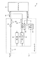
図3を参照すると、同期データ処理システムの一例の構成70が示されている。同期データ処理システム70は、データを格納するためのメモリモジュール72を備える。メモリコントローラ74は、メモリモジュール72に接続されている。示した実施形態では、メモリコントローラ74は、入力クロック信号(CLK_INT)78を受信し、反転クロック信号(CLK_OUT)80をメモリモジュール72へ送信するためのクロックインバータ76を備える。メモリコントローラ74がクロック生成器(図示せず)から入力クロック信号(CLK_INT)78を受信してもよい。
Referring to FIG. 3, an
反転クロック信号(CLK_OUT)80によって、メモリモジュールに到達する前の第1の伝搬遅延がメモリクロック信号(MEM_CLK)82として与えられる。この一例の実施形態では、反転クロック信号(CLK_OUT)80は、データサンプリングのセットアップ時間およびホールド時間を増加させる。一例の実施形態では、反転クロック76は、メモリモジュール72に対するセットアップ時間およびホールド時間として約2分の1クロックサイクルを与えるので、書込動作時により良好なデータサンプリングウィンドウが提供される。
A first propagation delay before reaching the memory module is provided as a memory clock signal (MEM_CLK) 82 by the inverted clock signal (CLK_OUT) 80. In this example embodiment, the inverted clock signal (CLK_OUT) 80 increases the setup time and hold time for data sampling. In one example embodiment, the inverted
メモリコントローラ74は、メモリモジュール72に接続されている書込データバッファ84を備える。書込データバッファ84は、入力クロック信号(CLK_INT)78に応答してメモリモジュール72にデータを送信する。さらにまた、非同期先入れ先出し(ASYNC FIFO)バッファ86もメモリモジュール72に接続されている。ASYNC FIFOバッファ86は、
メモリクロック信号(MEM_CLK)82をASYNC FIFOバッファ86にフィードバックすることによって生成されるフィードバッククロック信号(CLK_IN)88に応答して、メモリモジュール72からデータを読み取る。この一例の実施形態では、メモリクロック(MEM_CLK)信号82は、ASYNC FIFO86がメモリモジュール72の近くにあるとき、ASYNC FIFO86に向けて送られる。
The
Data is read from the
書込動作時には、データ(IPDATA)は、入力クロック信号(CLK_INT)78の立ち上がりエッジにおいてメモリコントローラ74の書込データバッファ84から発生される。このデータは遅延して伝搬し、MEM_DATAとしてメモリモジュール72によって受信される。当業者には認められるように、クロックおよびデータ信号はメモリモジュール72まで同一の距離を移動するので、書込データバッファ84からメモリモジュール72に送信されるデータの伝搬遅延は、第1の伝搬遅延とほぼ等しい。これによって、正確な書込データサンプリングが行えるといった利点が存在する。
During the write operation, data (IPDATA) is generated from the
同様に、読取動作時には、メモリクロック信号(MEM_CLK)82の立ち上がりエッジに対応して、データ(MEM_DATA)がメモリモジュール72から発生される。このデータは遅延して伝搬し、IP_DATAとしてメモリコントローラ74のASYNC FIFOバッファ86によって受信される。この場合にも、メモリモジュール72からASYNC FIFOバッファ86によって受信されるデータの伝播遅延は、ASYNC FIFOバッファ86に到達する前のメモリ信号(MEM_CLK)82によって与えられる第2の伝播遅延と、ほぼ等しい。なお、クロックおよびデータによってメモリモジュール72からASYNC FIFOバッファ86にループバックされるクロックと等しい遅延が与えられる。
Similarly, during the reading operation, data (MEM_DATA) is generated from the
また、同期データ処理システム70、ASYNC FIFOバッファ86に接続されている検出器90を備える。示した実施形態では、データはパケットの形式で転送され、各パケットはセキュアデジタル(SD)プロトコルなどフレームの開始部および終了部を有する。検出器90は、メモリモジュール72から届いたパケットデータにおいてフレームの開始部を検出する。
In addition, a
データサンプリングモジュール92は、フィードバッククロック信号(CLK_IN)88に応答してASYNC FIFOバッファ86からデータサンプリングを開始するべく、検出器90およびASYNC FIFOバッファ86に接続されている。データサンプリングが開始されると、ASYNC FIFOバッファ86は、入力クロック信号(CLK_INT)78に応答してデータサンプリングモジュール92にデータを提供する。検出器90およびデータサンプリングモジュール92がパケット化されたデータをサンプリングする動作については図6に関連して以下に記載する。
図4には、図3の同期データ処理システム70におけるデータ読取および書込サイクルの一例のタイミング図を示す。示した実施形態では、メモリコントローラ74によって受信される入力クロック信号(CLK_INT)は、参照符号100によって表される。さらに、クロックインバータ76によって送信される反転クロック信号(CLK_OUT)は、参照符号102によって表される。さらにまた、メモリクロック信号(MEM_CLK)およびフィードバック信号(CLK_IN)サイクルは参照符号106,108によってそれぞれ表される。
FIG. 4 shows a timing diagram of an example of a data read and write cycle in the synchronous
さらに、メモリコントローラ74によって発生され書込動作時にメモリモジュール72によって受信されるデータ信号(WDATA)は、参照符号110,112によってそれぞれ表される。同様に、メモリモジュール72によって送信され読取動作時にメモリコントローラ74によって読み取られるデータ信号(RDATA)は、参照符号114,116によってそれぞれ表される。
Further, data signals (WDATA) generated by the
示したように、データ(IP_DATA)110は、入力クロック信号(CLK_INT)100の立ち上がりエッジ(これは反転クロック信号(CLK_OUT)サイクル102の立ち下がりエッジ(参照符号114によって表される))に相当する書込データバッファ84から発生される。示した実施形態では、例えば、参照符号116によって表されるように、反転クロック信号(CLK_OUT)102によって、メモリモジュール72に到達する前の約2分の1クロックサイクルの伝搬遅延がメモリクロック信号(MEM_CLK)104として与えられる。
As shown, data (IP_DATA) 110 corresponds to the rising edge of input clock signal (CLK_INT) 100 (this is the falling edge of inverted clock signal (CLK_OUT) cycle 102 (represented by reference numeral 114)). Generated from
読取動作時には、データ(MEM_DATA)114は、メモリクロック信号(MEM_CLK)106立ち上がりエッジ120に対応してメモリモジュール72から発生される。このデータは遅延して伝搬し、IP_DATA116としてメモリコントローラ74のASYNC FIFOバッファ86によって受信される。この場合にも、この例では、メモリモジュール72からASYNC FIFOバッファ86によって受信されるデータの伝播遅延は、約2分の1クロックサイクルであり、これは参照符号122によって表されているように、ASYNC FIFOバッファ86に到達する前のメモリ信号(MEM_CLK)82によって発生される伝播遅延と等しい。
During the read operation, data (MEM_DATA) 114 is generated from the
図5には、同期データ処理システム130の別の一例の構成を示す。この一例の実施形態では、メモリコントローラ74とメモリモジュール72との間で転送されるデータは、スタティック・ランダム・アクセス・メモリ(SRAM)に通常用いられる読取イネーブル信号または書込イネーブル信号などの有効化信号を含む。検出器90が、メモリモジュール72から受信されるデータの読取イネーブル(RD_EN)信号132などの有効化信号を検出する。
FIG. 5 shows a configuration of another example of the synchronous
検出器90は、メモリモジュール72からASYNC FIFOバッファ86にフィードバックされるフィードバッククロック信号88および有効化信号132に応答して、データサンプリングモジュール92にASYNC FIFOバッファ86からのデータのサンプリングを開始させる。この構成における検出器90およびデータサンプリングモジュール92の動作については図7に関連して記載する。
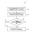
図6は、本発明による図3の同期データ処理システム70を用いるパケット化されたデータをサンプリングする方法140を示すフローチャートである。ブロック142において、フィードバッククロック信号88の立ち上がりエッジ(posedge)においてASYNC FIFOバッファにデータが送り込まれる。さらに、入力クロック信号に応答してASYNC FIFOバッファからのデータが検出器に供給される(ブロック144)。この一例の実施形態では、ASYNC FIFOバッファが空でないときには必ず、データが検出器に転送される。
FIG. 6 is a flowchart illustrating a
ブロック146において、検出器は、データの1から0への遷移をチェックすることによって、届いたパケット化データのフレームの開始部を検出する。フレームの開始部が検出される場合、ブロック148によって表されるように、トリガに従ってデータサンプリングモジュールはASYNC FIFOからのデータのサンプリングを開始する。あるいは、参照符号150によって表されるように、検出器はフレームの次の開始部を確認する。
In
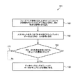
図7は、本発明による図5の同期データ処理システムを用いる有効化信号によってデータをサンプリングする方法160を示すフローチャートである。ブロック162において、データと、読取イネーブル(RD_EN)信号などの有効化信号とが、メモリモジュールからのフィードバック信号の立ち上がりエッジ(posedge)においてASYNC FIFOバッファに送り込まれる。さらに、入力クロック信号に応答して、ASYNC FIFOバッファからデータおよび読取イネーブル有効化信号が検出器に供給される(ブロック164)。この一例の実施形態では、ASYNC FIFOが空でないときには、データおよび読取イネーブル有効化信号が検出器に転送される。
FIG. 7 is a flowchart illustrating a
ブロック166において、検出器は、読取イネーブル有効化信号における1から0への遷移を検出する。読取イネーブル有効化信号が検出される場合、ブロック168によって表されるように、トリガに従ってデータサンプリングモジュールはASYNC FIFOからのデータのサンプリングを開始する。特定の実施形態では、データサンプリングはメモリアクセス時間の後に開始される。あるいは、参照符号170によって表されるように、検出器は次の読取イネーブル有効化信号を確認する。
In
本発明によって、上述のように、伝播遅延およびPVT条件にかかわらず、高信頼性のデータ転送が可能となる。上述のように、伝搬遅延およびPVT条件によって与えられる位相スキューを補償するデータ転送システムにおいて、メモリコントローラとメモリモジュールとの間で転送されるクロックとデータ信号との間に、確固たる関係が確立される。 As described above, the present invention enables highly reliable data transfer regardless of propagation delay and PVT conditions. As described above, in a data transfer system that compensates for phase skew provided by propagation delay and PVT conditions, a firm relationship is established between the clock and data signals transferred between the memory controller and the memory module. .
この技術では、書込データサンプリングを行うべくメモリモジュールに反転クロック信号を供給するための反転クロックが用いられる。また、この技術では、フィードバック信号を生成するべくメモリモジュールからのメモリクロック信号を送るクロック信号分配モジュールが用いられ、このクロック信号分配モジュールは、読取データサンプリングのためのASYNC FIFOバッファとともに用いられる。 In this technique, an inversion clock for supplying an inversion clock signal to the memory module is used to perform write data sampling. This technique also uses a clock signal distribution module that sends a memory clock signal from the memory module to generate a feedback signal, and this clock signal distribution module is used with an ASYNC FIFO buffer for read data sampling.
Claims (20)
データを格納するメモリモジュールと、
メモリモジュールに接続されているメモリコントローラとを備え、メモリコントローラは、
入力クロック信号を受信し、反転クロック信号をメモリモジュールに提供するクロックインバータであって、反転クロック信号によって、メモリモジュールに到達する前の第1の伝搬遅延がメモリクロック信号として与えられる、クロックインバータと、
メモリモジュールに接続されている書込データバッファであって、入力クロック信号に応答してメモリモジュールにデータを提供する、書込データバッファと、
メモリモジュールに接続されている非同期先入れ先出し(ASYNC FIFO)バッファであって、メモリクロック信号をASYNC FIFOバッファにフィードバックすることによって生成されるフィードバック信号に応答してメモリモジュールからデータを読み取る、ASYNC FIFOバッファと、を備える、同期データ処理システム。 A synchronous data processing system,
A memory module for storing data;
A memory controller connected to the memory module, the memory controller
A clock inverter that receives an input clock signal and provides an inverted clock signal to the memory module, wherein the inverted clock signal provides a first propagation delay as a memory clock signal before reaching the memory module; ,
A write data buffer connected to the memory module, the write data buffer providing data to the memory module in response to an input clock signal;
An asynchronous first-in first-out (ASYNC FIFO) buffer connected to the memory module, wherein the ASYNC FIFO buffer reads data from the memory module in response to a feedback signal generated by feeding back a memory clock signal to the ASYNC FIFO buffer; A synchronous data processing system.
データサンプリングモジュールであって、フィードバック信号に応答してASYNC FIFOバッファからのデータのサンプリングをデータサンプリングモジュールに開始させるべく、検出器およびASYNC FIFOバッファに接続されている、データサンプリングモジュールと、をさらに備える、請求項1に記載の同期データ処理システム。 A detector connected to the ASYNC FIFO buffer for detecting packet data received from the memory module;
A data sampling module, further comprising: a data sampling module coupled to the detector and the ASYNC FIFO buffer to cause the data sampling module to begin sampling data from the ASYNC FIFO buffer in response to the feedback signal The synchronous data processing system according to claim 1.
入力クロック信号を受信し、反転クロック信号をメモリモジュールに提供するためのクロックインバータであって、反転クロック信号によって、メモリモジュールに到達する前の第1の伝搬遅延がメモリクロック信号として与えられる、クロックインバータと、
クロック信号分配モジュールであって、メモリモジュールからメモリコントローラに向けてメモリクロック信号を送ることによってフィードバック信号を生成し、それによってメモリコントローラとメモリモジュールとの間で転送されるそれらのクロック信号がメモリモジュールとメモリコントローラとの間で送信されるデータと同じ位相遅延を有する、クロック信号分配モジュールと、を備える、メモリコントローラ。 In a memory controller used with a memory module of a synchronous data processing system,
A clock inverter for receiving an input clock signal and providing an inverted clock signal to the memory module, wherein the inverted clock signal provides a first propagation delay before reaching the memory module as the memory clock signal. An inverter;
A clock signal distribution module that generates a feedback signal by sending a memory clock signal from the memory module to the memory controller, thereby transferring those clock signals between the memory controller and the memory module. And a clock signal distribution module having the same phase delay as data transmitted between the memory controller and the memory controller.
入力クロック信号を受信するステップと、
メモリモジュールに対するメモリクロック信号を生成するべく、反転入力クロック信号をメモリモジュールに送信するステップと、
メモリモジュールからメモリコントローラにメモリクロック信号をフィードバックすることによってフィードバック信号を生成する工程であって、メモリコントローラとメモリモジュールとの間で転送されるクロック信号によってメモリモジュールとメモリコントローラとの間で送信されるデータと同じ位相遅延が与えられるステップと、を備える方法。 A method for transferring data between a memory module and a memory controller in a synchronous data processing system, comprising:
Receiving an input clock signal;
Transmitting an inverted input clock signal to the memory module to generate a memory clock signal for the memory module;
A step of generating a feedback signal by feeding back a memory clock signal from the memory module to the memory controller, and transmitted between the memory module and the memory controller by a clock signal transferred between the memory controller and the memory module. Providing the same phase delay as the data to be received.
メモリクロック信号を非同期先入れ先出し(ASYNC FIFO)バッファにフィードバックすることによって生成されるフィードバック信号に応答して、メモリモジュールからメモリコントローラのASYNC FIFOバッファにデータを送信するステップと、をさらに備える請求項17に記載の方法。 Transmitting data from the write data buffer of the memory controller to the memory module in response to the input clock signal;
The method further comprises: transmitting data from the memory module to the memory controller's ASYNC FIFO buffer in response to a feedback signal generated by feeding back the memory clock signal to an asynchronous first-in first-out (ASYNC FIFO) buffer. The method described.
入力クロック信号に応答してASYNC FIFOバッファからデータサンプリングモジュールにデータを提供するステップと、をさらに備える請求項18に記載の方法。 Initiating sampling of data received from the memory module in response to the feedback signal;
The method of claim 18, further comprising: providing data from the ASYNC FIFO buffer to the data sampling module in response to an input clock signal.
Applications Claiming Priority (2)
| Application Number | Priority Date | Filing Date | Title |
|---|---|---|---|
| US13/050,932 US8355294B2 (en) | 2011-03-18 | 2011-03-18 | Synchronous data processing system for reliable transfer of data irrespective of propagation delays and process, voltage and temperature (PVT) variations |
| US13/050,932 | 2011-03-18 |
Publications (1)
| Publication Number | Publication Date |
|---|---|
| JP2012198894A true JP2012198894A (en) | 2012-10-18 |
Family
ID=45939129
Family Applications (1)
| Application Number | Title | Priority Date | Filing Date |
|---|---|---|---|
| JP2012062441A Pending JP2012198894A (en) | 2011-03-18 | 2012-03-19 | Synchronous data processing system and method |
Country Status (6)
| Country | Link |
|---|---|
| US (1) | US8355294B2 (en) |
| EP (1) | EP2500826A3 (en) |
| JP (1) | JP2012198894A (en) |
| KR (1) | KR20120106638A (en) |
| CN (1) | CN102708074B (en) |
| TW (1) | TW201239895A (en) |
Families Citing this family (10)
| Publication number | Priority date | Publication date | Assignee | Title |
|---|---|---|---|---|
| CN101692346B (en) * | 2009-06-19 | 2013-06-26 | 无锡中星微电子有限公司 | Memory data sampling device and sampling controller |
| US9411722B2 (en) | 2013-03-04 | 2016-08-09 | Sandisk Technologies Llc | Asynchronous FIFO buffer for memory access |
| US9355691B2 (en) | 2014-06-29 | 2016-05-31 | Freescale Semiconductor, Inc. | Memory controller |
| US9251906B1 (en) * | 2015-05-18 | 2016-02-02 | Freescale Semiconductor, Inc. | Data strobe signal generation for flash memory |
| CN105893895A (en) * | 2016-03-31 | 2016-08-24 | 乐视控股(北京)有限公司 | Communication method and circuit for security digital cards |
| US10069496B1 (en) | 2017-05-02 | 2018-09-04 | Nxp Usa, Inc. | Circuit for compensating for both on and off-chip variations |
| US10949117B2 (en) * | 2018-09-24 | 2021-03-16 | Micron Technology, Inc. | Direct data transfer in memory and between devices of a memory module |
| CN111399802B (en) * | 2020-03-24 | 2022-08-19 | 飞腾信息技术有限公司 | Multi-power-domain multi-clock-domain first-in first-out queue, integrated circuit chip and computer equipment |
| US12019565B2 (en) * | 2022-06-30 | 2024-06-25 | Ampere Computing Llc | Advanced initialization bus (AIB) |
| CN115620797B (en) * | 2022-11-03 | 2025-12-19 | 芯动微电子科技(武汉)有限公司 | Method and device for acquiring and storing signal waveforms in chip based on AFIFO |
Family Cites Families (22)
| Publication number | Priority date | Publication date | Assignee | Title |
|---|---|---|---|---|
| US6003118A (en) | 1997-12-16 | 1999-12-14 | Acer Laboratories Inc. | Method and apparatus for synchronizing clock distribution of a data processing system |
| US6519688B1 (en) * | 2000-09-29 | 2003-02-11 | S3 Incorporated | Read data valid loop-back for high speed synchronized DRAM controller |
| US6496043B1 (en) * | 2001-12-13 | 2002-12-17 | Lsi Logic Corporation | Method and apparatus for measuring the phase of captured read data |
| US7418616B2 (en) * | 2002-07-15 | 2008-08-26 | Brooktree Broadband Holding, Inc. | System and method for improved synchronous data access |
| KR100510521B1 (en) * | 2003-03-04 | 2005-08-26 | 삼성전자주식회사 | Double data rate synchronous dynamic random access memory semiconductor device |
| US7430680B2 (en) * | 2005-01-19 | 2008-09-30 | Broadcom Corporation | System and method to align clock signals |
| US7464284B2 (en) | 2005-03-22 | 2008-12-09 | Hewlett-Packard Development Company, L.P. | Systems and methods for driving data over a bus where the systems employ a bus clock that is derived from a system clock and a data clock designed to lead the bus clock |
| US7436919B2 (en) | 2005-04-01 | 2008-10-14 | Freescale Semiconductor, Inc. | Methods and apparatus for bit synchronizing data transferred across a multi-pin asynchronous serial interface |
| TWI306343B (en) | 2005-09-01 | 2009-02-11 | Via Tech Inc | Bus receiver and method of deskewing bus signals |
| WO2007052091A1 (en) | 2005-11-02 | 2007-05-10 | Freescale Semiconductor, Inc. | Method and system for clock skew reduction in clock trees |
| US7711940B2 (en) | 2005-12-19 | 2010-05-04 | Samsung Electronics Co., Ltd. | Circuit block and circuit system having skew compensation, and skew compensation method |
| US7809085B2 (en) | 2006-01-19 | 2010-10-05 | Redmere Technology Ltd. | Data recovery system for source synchronous data channels |
| US7671579B1 (en) | 2006-03-09 | 2010-03-02 | Altera Corporation | Method and apparatus for quantifying and minimizing skew between signals |
| KR101206503B1 (en) | 2006-06-30 | 2012-11-29 | 삼성전자주식회사 | Circuit for removing skew and method for removing skew by the same |
| US7685454B2 (en) | 2006-07-12 | 2010-03-23 | Agere Systems Inc. | Signal buffering and retiming circuit for multiple memories |
| CN101118523B (en) * | 2006-08-01 | 2011-10-19 | 飞思卡尔半导体公司 | Memory access control device and method, memory access controller and method |
| US7590008B1 (en) | 2006-11-06 | 2009-09-15 | Altera Corporation | PVT compensated auto-calibration scheme for DDR3 |
| US7805627B2 (en) | 2007-03-29 | 2010-09-28 | Intel Corporation | Clock synchronization scheme for deskewing operations in a data interface |
| KR100910853B1 (en) | 2007-03-29 | 2009-08-06 | 주식회사 하이닉스반도체 | Semiconductor memory device and the method for operating the same |
| KR100907016B1 (en) | 2007-12-28 | 2009-07-08 | 주식회사 하이닉스반도체 | Data input circuit of semiconductor memory device and control method thereof |
| KR101022669B1 (en) * | 2008-12-02 | 2011-03-22 | 주식회사 하이닉스반도체 | Delay fixed loop circuit |
| CN101645301B (en) * | 2009-05-27 | 2013-06-12 | 无锡中星微电子有限公司 | Temperature self-adaptive adjustment method for read data sampling and device thereof |
-
2011
- 2011-03-18 US US13/050,932 patent/US8355294B2/en active Active
-
2012
- 2012-01-16 TW TW101101635A patent/TW201239895A/en unknown
- 2012-02-22 CN CN201210042210.8A patent/CN102708074B/en active Active
- 2012-03-16 KR KR1020120027035A patent/KR20120106638A/en not_active Withdrawn
- 2012-03-16 EP EP12159924.5A patent/EP2500826A3/en not_active Withdrawn
- 2012-03-19 JP JP2012062441A patent/JP2012198894A/en active Pending
Also Published As
| Publication number | Publication date |
|---|---|
| KR20120106638A (en) | 2012-09-26 |
| EP2500826A3 (en) | 2014-06-11 |
| US8355294B2 (en) | 2013-01-15 |
| US20120239961A1 (en) | 2012-09-20 |
| EP2500826A2 (en) | 2012-09-19 |
| CN102708074A (en) | 2012-10-03 |
| TW201239895A (en) | 2012-10-01 |
| CN102708074B (en) | 2016-07-06 |
Similar Documents
| Publication | Publication Date | Title |
|---|---|---|
| JP2012198894A (en) | Synchronous data processing system and method | |
| JP4219949B2 (en) | Synchronous memory device | |
| US8788780B2 (en) | Signal restoration circuit, latency adjustment circuit, memory controller, processor, computer, signal restoration method, and latency adjustment method | |
| JP2004506974A (en) | System and method for synchronizing skip patterns and initializing a clock feed interface in a multiple clock system | |
| JP4998699B2 (en) | Semiconductor device and communication control method | |
| CN100555263C (en) | Serializer for generating serial clock and method for serial data transmission | |
| JP2009147869A (en) | Synchronization circuit | |
| KR100624261B1 (en) | Device and method of data entry | |
| US9213359B2 (en) | Interface for controlling the phase alignment of clock signals for a recipient device | |
| CN105610532B (en) | Signal transmission and processing method, device and equipment | |
| JPH0358263A (en) | Synchronizer using clock phase extrapolation | |
| JP6413585B2 (en) | Transmission circuit, integrated circuit, and parallel-serial conversion method | |
| JP4598872B2 (en) | Timing recovery circuit, communication node, network system, and electronic device | |
| US7499368B2 (en) | Variable clocking read capture for double data rate memory devices | |
| US6810486B2 (en) | Method and apparatus for de-skewing a clock using a first and second phase locked loop and a clock tree | |
| EP1317085B1 (en) | A method and circuit for initializing a de-skewing buffer in a clock forwarded system | |
| US7248661B1 (en) | Data transfer between phase independent clock domains | |
| US7793021B2 (en) | Method for synchronizing a transmission of information and a device having synchronizing capabilities | |
| KR100656462B1 (en) | Circuit and Method for Generating Data Output Clock of Semiconductor Memory Device | |
| JPH11161601A (en) | Adjustment device for delay time between multiple transmission lines | |
| JP5926583B2 (en) | Information processing apparatus, serial communication system, communication initialization method thereof, and serial communication apparatus | |
| JP3604637B2 (en) | Asynchronous transfer device and asynchronous transfer method | |
| JP3562416B2 (en) | Inter-LSI data transfer system and source synchronous data transfer method used therefor | |
| US20090232266A1 (en) | Signal processing device | |
| JP5921264B2 (en) | Serial communication system and communication initialization method thereof, and serial communication apparatus and communication initialization method thereof |