JP2012198975A - ローカル列デコーダに関連付けられた互い違いに配置されたセンスアンプを有する半導体メモリ - Google Patents
ローカル列デコーダに関連付けられた互い違いに配置されたセンスアンプを有する半導体メモリ Download PDFInfo
- Publication number
- JP2012198975A JP2012198975A JP2011273544A JP2011273544A JP2012198975A JP 2012198975 A JP2012198975 A JP 2012198975A JP 2011273544 A JP2011273544 A JP 2011273544A JP 2011273544 A JP2011273544 A JP 2011273544A JP 2012198975 A JP2012198975 A JP 2012198975A
- Authority
- JP
- Japan
- Prior art keywords
- sense amplifier
- semiconductor memory
- bank
- metal
- electrically coupled
- Prior art date
- Legal status (The legal status is an assumption and is not a legal conclusion. Google has not performed a legal analysis and makes no representation as to the accuracy of the status listed.)
- Granted
Links
Images




Classifications
-
- G—PHYSICS
- G11—INFORMATION STORAGE
- G11C—STATIC STORES
- G11C11/00—Digital stores characterised by the use of particular electric or magnetic storage elements; Storage elements therefor
- G11C11/21—Digital stores characterised by the use of particular electric or magnetic storage elements; Storage elements therefor using electric elements
- G11C11/34—Digital stores characterised by the use of particular electric or magnetic storage elements; Storage elements therefor using electric elements using semiconductor devices
- G11C11/40—Digital stores characterised by the use of particular electric or magnetic storage elements; Storage elements therefor using electric elements using semiconductor devices using transistors
- G11C11/401—Digital stores characterised by the use of particular electric or magnetic storage elements; Storage elements therefor using electric elements using semiconductor devices using transistors forming cells needing refreshing or charge regeneration, i.e. dynamic cells
- G11C11/4063—Auxiliary circuits, e.g. for addressing, decoding, driving, writing, sensing or timing
- G11C11/407—Auxiliary circuits, e.g. for addressing, decoding, driving, writing, sensing or timing for memory cells of the field-effect type
- G11C11/409—Read-write [R-W] circuits
- G11C11/4091—Sense or sense/refresh amplifiers, or associated sense circuitry, e.g. for coupled bit-line precharging, equalising or isolating
-
- G—PHYSICS
- G11—INFORMATION STORAGE
- G11C—STATIC STORES
- G11C11/00—Digital stores characterised by the use of particular electric or magnetic storage elements; Storage elements therefor
- G11C11/21—Digital stores characterised by the use of particular electric or magnetic storage elements; Storage elements therefor using electric elements
- G11C11/34—Digital stores characterised by the use of particular electric or magnetic storage elements; Storage elements therefor using electric elements using semiconductor devices
- G11C11/40—Digital stores characterised by the use of particular electric or magnetic storage elements; Storage elements therefor using electric elements using semiconductor devices using transistors
- G11C11/401—Digital stores characterised by the use of particular electric or magnetic storage elements; Storage elements therefor using electric elements using semiconductor devices using transistors forming cells needing refreshing or charge regeneration, i.e. dynamic cells
- G11C11/4063—Auxiliary circuits, e.g. for addressing, decoding, driving, writing, sensing or timing
- G11C11/407—Auxiliary circuits, e.g. for addressing, decoding, driving, writing, sensing or timing for memory cells of the field-effect type
- G11C11/409—Read-write [R-W] circuits
- G11C11/4096—Input/output [I/O] data management or control circuits, e.g. reading or writing circuits, I/O drivers or bit-line switches
-
- G—PHYSICS
- G11—INFORMATION STORAGE
- G11C—STATIC STORES
- G11C11/00—Digital stores characterised by the use of particular electric or magnetic storage elements; Storage elements therefor
- G11C11/21—Digital stores characterised by the use of particular electric or magnetic storage elements; Storage elements therefor using electric elements
- G11C11/34—Digital stores characterised by the use of particular electric or magnetic storage elements; Storage elements therefor using electric elements using semiconductor devices
- G11C11/40—Digital stores characterised by the use of particular electric or magnetic storage elements; Storage elements therefor using electric elements using semiconductor devices using transistors
- G11C11/401—Digital stores characterised by the use of particular electric or magnetic storage elements; Storage elements therefor using electric elements using semiconductor devices using transistors forming cells needing refreshing or charge regeneration, i.e. dynamic cells
- G11C11/4063—Auxiliary circuits, e.g. for addressing, decoding, driving, writing, sensing or timing
- G11C11/407—Auxiliary circuits, e.g. for addressing, decoding, driving, writing, sensing or timing for memory cells of the field-effect type
- G11C11/409—Read-write [R-W] circuits
- G11C11/4097—Bit-line organisation, e.g. bit-line layout, folded bit lines
-
- G—PHYSICS
- G11—INFORMATION STORAGE
- G11C—STATIC STORES
- G11C7/00—Arrangements for writing information into, or reading information out from, a digital store
- G11C7/06—Sense amplifiers; Associated circuits, e.g. timing or triggering circuits
- G11C7/065—Differential amplifiers of latching type
Landscapes
- Engineering & Computer Science (AREA)
- Microelectronics & Electronic Packaging (AREA)
- Computer Hardware Design (AREA)
- Databases & Information Systems (AREA)
- Dram (AREA)
- Semiconductor Memories (AREA)
Abstract
【解決手段】本発明は、半導体メモリであって、ビット線と、メモリセルアレイと、少なくとも1組のセンスアンプバンクであって、各センスアンプは、交互の配列により、対応するビット線に接続されていることによって、ビット線と平行な各センスアンプバンクの組で利用可能なスペースに相互接続することを備え、各センスアンプバンクは、センスアンプバンクの少なくとも1つのセンスアンプを選択する、少なくとも1つのローカル列デコーダを備え、前記ローカル列デコーダは、ビット線と平行な利用可能な相互接続スペース内に走っている出力線によってセンスアンプバンクの少なくとも1つのセンスアンプと電気的に結合されたことを特徴とする半導体メモリに関するものである。
【選択図】図3
Description
―各センスアンプバンクは、前記センスアンプバンクの各センスアンプと電気的に結合した単一のローカル列デコーダを備えたこと
―各センスアンプバンクは、複数のローカル列デコーダを備えたこと、
―前記ローカル列デコーダは、NORゲート又はNANDゲートであること、
―前記ローカル列デコーダは、複数のデコーダセクションを備え、各デコーダセクションは、前記センスアンプバンクのそれぞれのセンスアンプと電気的に結合されたこと、
―前記センスアンプバンクは、SOI基板上に実装され、デコーダセクションは、接地とデコーダセクションの第1の入力との間に連続して2つのコンプリメンタリダブルゲートトランジスタを有している擬似インバータを備え、各ダブルゲートトランジスタは、第1のゲートと第2のゲートを有し、トランジスタの第1のゲートは、トランジスタの第2のゲートが第1の入力の補完に電気的に結合されている場合、デコーダセクションの第2の入力に電気的に結合され、デコーダセクションの出力は、2つのトランジスタのひと続きの関連の中点に供給されていること、
―前記ローカル列デコーダの第1の入力は、第1の入力線によって第1の列アドレスバスに接続され、前記ローカル列デコーダの第2の入力は、第2の入力線によって第2の列アドレスバスに接続され、第1及び第2の入力線は、利用できる相互接続のスペース内に走ること
―第1の入力線は、メタル―0線及びメタル―1バスである第1の列アドレスバスであること、
―第2の入力線は、メタル―0線及びメタル―1バスである第2の列アドレスバスであること、
―第2の入力線は、メタル―0線であり、第2の列アドレスバスは、ビット線の長手方向へ走っているメタル―2バス及びメタル―2バスに電気的に結合されたメタル―1バスを備え、ワード線の横方向へ走っているメタル―1バスを備えたこと、である。
Claims (10)
- 半導体メモリであって、
それぞれが交差する複数のビット線及び複数のワード線と、
前記ビット線及び前記ワード線のクロスポイントで列と行に整列された複数のメモリセルによって形成されたメモリセルアレイと、
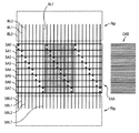
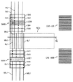
前記メモリセルアレイの反対側に整列された少なくとも1組のセンスアンプバンクであって、各センスアンプバンクの組は、ビット線の長手方向に互い違いに配置された複数のセンスアンプを備え、各センスアンプは、交互の配列により、対応するビット線に接続されていることによって、ビット線は、1組の第1のバンクのセンスアンプに電気的に結合されたビット線と、1組の第2のバンクのセンスアンプに電気的に結合されたビット線との間を横方向へ行ったり来たりして、ビット線の交互配列が、ビット線と平行な各センスアンプバンクの組で利用可能なスペースに相互接続することとを備え、
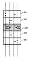
各センスアンプバンクは、センスアンプバンクの少なくとも1つのセンスアンプを選択する、少なくとも1つのローカル列デコーダを備え、前記ローカル列デコーダは、センスアンプと共に互い違いに配置され、ビット線と平行な利用可能な相互接続スペース内に走っている出力線によってセンスアンプバンクの少なくとも1つのセンスアンプと電気的に結合されたことを特徴とする半導体メモリ。 - 各センスアンプバンクは、前記センスアンプバンクの各センスアンプに電気的に結合した単一のローカル列デコーダを備えたことを特徴とする請求項1に記載の半導体メモリ。
- 各センスアンプバンクは、複数のローカル列デコーダを備えたことを特徴とする請求項1に記載の半導体メモリ。
- 前記ローカル列デコーダは、NORゲート又はNANDゲートであることを特徴とする請求項1から3のいずれかに記載の半導体メモリ。
- 前記ローカル列デコーダは、複数のデコーダセクションを備え、各デコーダセクションは、前記センスアンプバンクのそれぞれのセンスアンプと電気的に結合されたことを特徴とする請求項1から4のいずれかに記載の半導体メモリ。
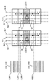
- 前記センスアンプバンクは、SOI基板上に実装され、デコーダセクションは、接地とデコーダセクションの第1の入力との間に連続して2つのコンプリメンタリダブルゲートトランジスタを有している擬似インバータを備え、各ダブルゲートトランジスタは、第1のゲートと第2のゲートを有し、トランジスタの第1のゲートは、トランジスタの第2のゲートが第1の入力の補完に電気的に結合されている場合、デコーダセクションの第2の入力に電気的に結合され、デコーダセクションの出力は、2つのトランジスタのひと続きの関連の中点に供給されていることを特徴とする請求項5に記載の半導体メモリ。
- 前記ローカル列デコーダの第1の入力は、第1の入力線によって第1の列アドレスバスに接続され、前記ローカル列デコーダの第2の入力は、第2の入力線によって第2の列アドレスバスに接続され、第1及び第2の入力線は、利用できる相互接続のスペース内に走ることを特徴とする請求項1から6のいずれかに記載の半導体メモリ。
- 第1の入力線は、メタル―0線及びメタル―1バスである第1の列アドレスバスであることを特徴とする請求項7に記載の半導体メモリ。
- 第2の入力線は、メタル―0線及びメタル―1バスである第2の列アドレスバスであることを特徴とする請求項7または8に記載の半導体メモリ。
- 第2の入力線は、メタル―0線であり、第2の列アドレスバスは、ビット線の長手方向へ走っているメタル―2バス及びメタル―2バスに電気的に結合されたメタル―1バスを備え、ワード線の横方向へ走っているメタル―1バスを備えたことを特徴とする請求項7または8に記載の半導体メモリ。
Applications Claiming Priority (2)
| Application Number | Priority Date | Filing Date | Title |
|---|---|---|---|
| FR1152256A FR2972838B1 (fr) | 2011-03-18 | 2011-03-18 | Memoire a semi-conducteurs comportant des amplificateurs de lecture decales associes a un decodeur de colonne local |
| FR1152256 | 2011-03-18 |
Publications (2)
| Publication Number | Publication Date |
|---|---|
| JP2012198975A true JP2012198975A (ja) | 2012-10-18 |
| JP5524942B2 JP5524942B2 (ja) | 2014-06-18 |
Family
ID=45093637
Family Applications (1)
| Application Number | Title | Priority Date | Filing Date |
|---|---|---|---|
| JP2011273544A Active JP5524942B2 (ja) | 2011-03-18 | 2011-12-14 | ローカル列デコーダに関連付けられた互い違いに配置されたセンスアンプを有する半導体メモリ |
Country Status (8)
| Country | Link |
|---|---|
| US (1) | US9159400B2 (ja) |
| EP (1) | EP2500906B1 (ja) |
| JP (1) | JP5524942B2 (ja) |
| KR (1) | KR101334284B1 (ja) |
| CN (1) | CN102682833B (ja) |
| FR (1) | FR2972838B1 (ja) |
| SG (1) | SG184623A1 (ja) |
| TW (1) | TWI485704B (ja) |
Families Citing this family (12)
| Publication number | Priority date | Publication date | Assignee | Title |
|---|---|---|---|---|
| FR2982700B1 (fr) | 2011-11-15 | 2014-02-07 | Soitec Silicon On Insulator | Amplificateur de lecture avec transistors de precharge et de decodage a grille double |
| KR20140146369A (ko) | 2013-06-17 | 2014-12-26 | 에스케이하이닉스 주식회사 | 반도체 메모리 장치 및 메모리 시스템 |
| US9972395B2 (en) * | 2015-10-05 | 2018-05-15 | Silicon Storage Technology, Inc. | Row and column decoders comprising fully depleted silicon-on-insulator transistors for use in flash memory systems |
| US11087827B1 (en) | 2020-02-07 | 2021-08-10 | Micron Technology, Inc. | Edge memory array mats with sense amplifiers |
| US12217784B2 (en) * | 2020-03-19 | 2025-02-04 | Rambus Inc. | Boosted writeback voltage |
| US11024366B1 (en) * | 2020-04-24 | 2021-06-01 | Micron Technology, Inc. | Under-memory array process edge mats with sense amplifiers |
| EP4231301B1 (en) * | 2020-09-18 | 2025-07-16 | Changxin Memory Technologies, Inc. | Bit line sense circuit and memory |
| CN114203230B (zh) * | 2020-09-18 | 2023-09-15 | 长鑫存储技术有限公司 | 一种列选择信号单元电路、位线感测电路及存储器 |
| CN114203247B (zh) * | 2020-09-18 | 2024-03-26 | 长鑫存储技术有限公司 | 一种位线感测电路及存储器 |
| JP2023008403A (ja) * | 2021-07-06 | 2023-01-19 | キオクシア株式会社 | 半導体集積回路 |
| TWI873776B (zh) * | 2022-08-12 | 2025-02-21 | 愛普科技股份有限公司 | 具有分段式資料線結構的記憶體裝置 |
| US12482520B2 (en) * | 2022-11-23 | 2025-11-25 | The Trustees Of Columbia University In The City Of New York | 6T-SRAM-based digital computing-in-memory circuits supporting flexible input dimension |
Citations (8)
| Publication number | Priority date | Publication date | Assignee | Title |
|---|---|---|---|---|
| JPH02123596A (ja) * | 1988-11-02 | 1990-05-11 | Nec Corp | 半導体メモリー |
| JPH03108750A (ja) * | 1989-06-26 | 1991-05-08 | Nec Corp | 半導体記憶集積回路 |
| JPH04252491A (ja) * | 1991-01-28 | 1992-09-08 | Nec Corp | 半導体メモリ |
| JPH05182457A (ja) * | 1991-12-26 | 1993-07-23 | Toshiba Corp | ダイナミック型半導体記憶装置 |
| JPH06162771A (ja) * | 1992-11-20 | 1994-06-10 | Sanyo Electric Co Ltd | 半導体記憶装置 |
| JPH06275826A (ja) * | 1993-03-24 | 1994-09-30 | Fujitsu Ltd | 半導体装置 |
| JPH08172169A (ja) * | 1994-12-16 | 1996-07-02 | Toshiba Microelectron Corp | 半導体記憶装置 |
| JP2002026294A (ja) * | 2000-07-10 | 2002-01-25 | Hitachi Ltd | 半導体集積回路装置 |
Family Cites Families (24)
| Publication number | Priority date | Publication date | Assignee | Title |
|---|---|---|---|---|
| JPS57208691A (en) * | 1981-06-15 | 1982-12-21 | Mitsubishi Electric Corp | Semiconductor memory |
| JPS5880189A (ja) * | 1981-11-05 | 1983-05-14 | Fujitsu Ltd | 半導体記憶装置 |
| JPS6413290A (en) * | 1987-07-07 | 1989-01-18 | Oki Electric Ind Co Ltd | Semiconductor memory |
| DE3937068C2 (de) * | 1988-11-07 | 1994-10-06 | Toshiba Kawasaki Kk | Dynamische Halbleiterspeicheranordnung |
| KR100224769B1 (ko) * | 1995-12-29 | 1999-10-15 | 김영환 | 고속 버스트 리드/라이트 동작에 적합한 데이타 버스 라인 구조를 갖는 반도체 메모리 장치 |
| US5666324A (en) * | 1996-03-15 | 1997-09-09 | Mitsubishi Denki Kabushiki Kaisha | Clock synchronous semiconductor memory device having current consumption reduced |
| KR100200312B1 (ko) * | 1996-11-13 | 1999-06-15 | 김영환 | 반도체 소자의 비트 라인 센스 앰프와 데이타 버스 라인 연결 방법 |
| JP3863968B2 (ja) * | 1997-06-10 | 2006-12-27 | 株式会社ルネサステクノロジ | 半導体記憶装置 |
| US5822268A (en) * | 1997-09-11 | 1998-10-13 | International Business Machines Corporation | Hierarchical column select line architecture for multi-bank DRAMs |
| KR100252053B1 (ko) * | 1997-12-04 | 2000-05-01 | 윤종용 | 칼럼 방향의 데이터 입출력선을 가지는 반도체메모리장치와불량셀 구제회로 및 방법 |
| DE19915081C2 (de) * | 1999-04-01 | 2001-10-18 | Infineon Technologies Ag | Integrierter Speicher, dessen Speicherzellen mit Plattenleitungen verbunden sind |
| KR100732287B1 (ko) * | 1999-04-08 | 2007-06-25 | 주식회사 하이닉스반도체 | 패킷 명령어 구동형 반도체 메모리 장치 |
| JP4427847B2 (ja) * | 1999-11-04 | 2010-03-10 | エルピーダメモリ株式会社 | ダイナミック型ramと半導体装置 |
| JP4353621B2 (ja) * | 2000-06-30 | 2009-10-28 | 株式会社ルネサステクノロジ | 半導体装置 |
| KR100384559B1 (ko) * | 2000-06-30 | 2003-05-22 | 주식회사 하이닉스반도체 | 반도체 메모리 소자의 컬럼 디코딩 장치 |
| JP4044401B2 (ja) * | 2002-09-11 | 2008-02-06 | 株式会社東芝 | 半導体記憶装置 |
| KR100587692B1 (ko) * | 2004-11-05 | 2006-06-08 | 삼성전자주식회사 | 반도체 메모리 장치에서의 회로 배선 배치구조와 그에따른 배치방법 |
| JP2007109272A (ja) * | 2005-10-11 | 2007-04-26 | Elpida Memory Inc | 半導体記憶装置 |
| KR100666181B1 (ko) * | 2005-12-27 | 2007-01-09 | 삼성전자주식회사 | 센스앰프 및 워드라인 드라이버 영역을 위한 면적을최소화하는 레이아웃을 가지는 반도체 메모리 장치 |
| DE102007012902B3 (de) * | 2007-03-19 | 2008-07-10 | Qimonda Ag | Kopplungsoptimierte Anschlusskonfiguration von Signalleitungen und Verstärkern |
| KR101398635B1 (ko) * | 2008-11-11 | 2014-05-22 | 삼성전자주식회사 | 센스 앰프를 공유하는 반도체 메모리 장치 |
| US8320178B2 (en) * | 2009-07-02 | 2012-11-27 | Actel Corporation | Push-pull programmable logic device cell |
| FR2958441B1 (fr) * | 2010-04-02 | 2012-07-13 | Soitec Silicon On Insulator | Circuit pseudo-inverseur sur seoi |
| EP2372716A1 (en) | 2010-04-02 | 2011-10-05 | S.O.I.Tec Silicon on Insulator Technologies | Pseudo-inverter circuit on SeOI |
-
2011
- 2011-03-18 FR FR1152256A patent/FR2972838B1/fr not_active Expired - Fee Related
- 2011-12-13 KR KR1020110133670A patent/KR101334284B1/ko active Active
- 2011-12-13 EP EP11193263.8A patent/EP2500906B1/en active Active
- 2011-12-13 SG SG2011092053A patent/SG184623A1/en unknown
- 2011-12-14 TW TW100146174A patent/TWI485704B/zh active
- 2011-12-14 JP JP2011273544A patent/JP5524942B2/ja active Active
- 2011-12-14 CN CN201110416792.7A patent/CN102682833B/zh active Active
-
2012
- 2012-03-16 US US13/422,697 patent/US9159400B2/en active Active
Patent Citations (8)
| Publication number | Priority date | Publication date | Assignee | Title |
|---|---|---|---|---|
| JPH02123596A (ja) * | 1988-11-02 | 1990-05-11 | Nec Corp | 半導体メモリー |
| JPH03108750A (ja) * | 1989-06-26 | 1991-05-08 | Nec Corp | 半導体記憶集積回路 |
| JPH04252491A (ja) * | 1991-01-28 | 1992-09-08 | Nec Corp | 半導体メモリ |
| JPH05182457A (ja) * | 1991-12-26 | 1993-07-23 | Toshiba Corp | ダイナミック型半導体記憶装置 |
| JPH06162771A (ja) * | 1992-11-20 | 1994-06-10 | Sanyo Electric Co Ltd | 半導体記憶装置 |
| JPH06275826A (ja) * | 1993-03-24 | 1994-09-30 | Fujitsu Ltd | 半導体装置 |
| JPH08172169A (ja) * | 1994-12-16 | 1996-07-02 | Toshiba Microelectron Corp | 半導体記憶装置 |
| JP2002026294A (ja) * | 2000-07-10 | 2002-01-25 | Hitachi Ltd | 半導体集積回路装置 |
Also Published As
| Publication number | Publication date |
|---|---|
| SG184623A1 (en) | 2012-10-30 |
| TWI485704B (zh) | 2015-05-21 |
| US20120243360A1 (en) | 2012-09-27 |
| EP2500906A1 (en) | 2012-09-19 |
| KR20120106540A (ko) | 2012-09-26 |
| CN102682833A (zh) | 2012-09-19 |
| JP5524942B2 (ja) | 2014-06-18 |
| CN102682833B (zh) | 2014-12-10 |
| US9159400B2 (en) | 2015-10-13 |
| FR2972838B1 (fr) | 2013-04-12 |
| TW201239885A (en) | 2012-10-01 |
| KR101334284B1 (ko) | 2013-11-29 |
| EP2500906B1 (en) | 2014-02-12 |
| FR2972838A1 (fr) | 2012-09-21 |
Similar Documents
| Publication | Publication Date | Title |
|---|---|---|
| JP5524942B2 (ja) | ローカル列デコーダに関連付けられた互い違いに配置されたセンスアンプを有する半導体メモリ | |
| US5499215A (en) | Semiconductor memory | |
| JP5666108B2 (ja) | 半導体装置及びこれを備えるシステム | |
| JP4574136B2 (ja) | 半導体集積回路装置 | |
| US7161823B2 (en) | Semiconductor memory device and method of arranging signal and power lines thereof | |
| JP7013359B2 (ja) | 半導体装置及びデータ保持方法 | |
| US6125070A (en) | Semiconductor memory device having multiple global I/O line pairs | |
| JP5612803B2 (ja) | 半導体記憶装置 | |
| KR100215602B1 (ko) | 반도체 기억장치 | |
| US8976563B2 (en) | Semiconductor memory device | |
| JP2009033029A (ja) | 半導体記憶装置 | |
| JP5642983B2 (ja) | 半導体装置 | |
| JP2003007852A (ja) | 半導体記憶装置 | |
| CN103930949B (zh) | 具有双栅预充电和解码晶体管的读出放大器 | |
| US6768143B1 (en) | Structure and method of making three finger folded field effect transistors having shared junctions | |
| JP6029434B2 (ja) | 半導体記憶装置 | |
| JP4011248B2 (ja) | 半導体記憶装置 | |
| US6838337B2 (en) | Sense amplifier and architecture for open digit arrays | |
| JPH10303389A (ja) | 半導体メモリ装置 | |
| JP2003077277A (ja) | 半導体記憶装置 | |
| JP2001266569A (ja) | 半導体記憶装置 |
Legal Events
| Date | Code | Title | Description |
|---|---|---|---|
| A977 | Report on retrieval |
Free format text: JAPANESE INTERMEDIATE CODE: A971007 Effective date: 20130208 |
|
| A131 | Notification of reasons for refusal |
Free format text: JAPANESE INTERMEDIATE CODE: A131 Effective date: 20130226 |
|
| A601 | Written request for extension of time |
Free format text: JAPANESE INTERMEDIATE CODE: A601 Effective date: 20130524 |
|
| A602 | Written permission of extension of time |
Free format text: JAPANESE INTERMEDIATE CODE: A602 Effective date: 20130529 |
|
| A601 | Written request for extension of time |
Free format text: JAPANESE INTERMEDIATE CODE: A601 Effective date: 20130626 |
|
| A602 | Written permission of extension of time |
Free format text: JAPANESE INTERMEDIATE CODE: A602 Effective date: 20130701 |
|
| A601 | Written request for extension of time |
Free format text: JAPANESE INTERMEDIATE CODE: A601 Effective date: 20130726 |
|
| A602 | Written permission of extension of time |
Free format text: JAPANESE INTERMEDIATE CODE: A602 Effective date: 20130731 |
|
| A521 | Request for written amendment filed |
Free format text: JAPANESE INTERMEDIATE CODE: A523 Effective date: 20130826 |
|
| TRDD | Decision of grant or rejection written | ||
| A01 | Written decision to grant a patent or to grant a registration (utility model) |
Free format text: JAPANESE INTERMEDIATE CODE: A01 Effective date: 20140311 |
|
| A61 | First payment of annual fees (during grant procedure) |
Free format text: JAPANESE INTERMEDIATE CODE: A61 Effective date: 20140410 |
|
| R150 | Certificate of patent or registration of utility model |
Ref document number: 5524942 Country of ref document: JP Free format text: JAPANESE INTERMEDIATE CODE: R150 |
|
| R250 | Receipt of annual fees |
Free format text: JAPANESE INTERMEDIATE CODE: R250 |
|
| R250 | Receipt of annual fees |
Free format text: JAPANESE INTERMEDIATE CODE: R250 |
|
| R250 | Receipt of annual fees |
Free format text: JAPANESE INTERMEDIATE CODE: R250 |
|
| R250 | Receipt of annual fees |
Free format text: JAPANESE INTERMEDIATE CODE: R250 |
|
| R250 | Receipt of annual fees |
Free format text: JAPANESE INTERMEDIATE CODE: R250 |
|
| R250 | Receipt of annual fees |
Free format text: JAPANESE INTERMEDIATE CODE: R250 |
|
| R250 | Receipt of annual fees |
Free format text: JAPANESE INTERMEDIATE CODE: R250 |
|
| R250 | Receipt of annual fees |
Free format text: JAPANESE INTERMEDIATE CODE: R250 |
|
| R250 | Receipt of annual fees |
Free format text: JAPANESE INTERMEDIATE CODE: R250 |
|
| R250 | Receipt of annual fees |
Free format text: JAPANESE INTERMEDIATE CODE: R250 |