JP2012199520A - 半導体装置およびその製造方法 - Google Patents
半導体装置およびその製造方法 Download PDFInfo
- Publication number
- JP2012199520A JP2012199520A JP2012036376A JP2012036376A JP2012199520A JP 2012199520 A JP2012199520 A JP 2012199520A JP 2012036376 A JP2012036376 A JP 2012036376A JP 2012036376 A JP2012036376 A JP 2012036376A JP 2012199520 A JP2012199520 A JP 2012199520A
- Authority
- JP
- Japan
- Prior art keywords
- layer
- plane
- face
- centered cubic
- catalyst layer
- Prior art date
- Legal status (The legal status is an assumption and is not a legal conclusion. Google has not performed a legal analysis and makes no representation as to the accuracy of the status listed.)
- Pending
Links
Images






Classifications
-
- H—ELECTRICITY
- H10—SEMICONDUCTOR DEVICES; ELECTRIC SOLID-STATE DEVICES NOT OTHERWISE PROVIDED FOR
- H10P—GENERIC PROCESSES OR APPARATUS FOR THE MANUFACTURE OR TREATMENT OF DEVICES COVERED BY CLASS H10
- H10P14/00—Formation of materials, e.g. in the shape of layers or pillars
- H10P14/20—Formation of materials, e.g. in the shape of layers or pillars of semiconductor materials
- H10P14/27—Formation of materials, e.g. in the shape of layers or pillars of semiconductor materials using selective deposition, e.g. simultaneous growth of monocrystalline and non-monocrystalline semiconductor materials
- H10P14/271—Formation of materials, e.g. in the shape of layers or pillars of semiconductor materials using selective deposition, e.g. simultaneous growth of monocrystalline and non-monocrystalline semiconductor materials characterised by the preparation of substrate for selective deposition
-
- H—ELECTRICITY
- H10—SEMICONDUCTOR DEVICES; ELECTRIC SOLID-STATE DEVICES NOT OTHERWISE PROVIDED FOR
- H10P—GENERIC PROCESSES OR APPARATUS FOR THE MANUFACTURE OR TREATMENT OF DEVICES COVERED BY CLASS H10
- H10P14/00—Formation of materials, e.g. in the shape of layers or pillars
- H10P14/20—Formation of materials, e.g. in the shape of layers or pillars of semiconductor materials
- H10P14/27—Formation of materials, e.g. in the shape of layers or pillars of semiconductor materials using selective deposition, e.g. simultaneous growth of monocrystalline and non-monocrystalline semiconductor materials
- H10P14/271—Formation of materials, e.g. in the shape of layers or pillars of semiconductor materials using selective deposition, e.g. simultaneous growth of monocrystalline and non-monocrystalline semiconductor materials characterised by the preparation of substrate for selective deposition
- H10P14/274—Formation of materials, e.g. in the shape of layers or pillars of semiconductor materials using selective deposition, e.g. simultaneous growth of monocrystalline and non-monocrystalline semiconductor materials characterised by the preparation of substrate for selective deposition using seed materials
-
- H—ELECTRICITY
- H10—SEMICONDUCTOR DEVICES; ELECTRIC SOLID-STATE DEVICES NOT OTHERWISE PROVIDED FOR
- H10P—GENERIC PROCESSES OR APPARATUS FOR THE MANUFACTURE OR TREATMENT OF DEVICES COVERED BY CLASS H10
- H10P14/00—Formation of materials, e.g. in the shape of layers or pillars
- H10P14/20—Formation of materials, e.g. in the shape of layers or pillars of semiconductor materials
- H10P14/32—Formation of materials, e.g. in the shape of layers or pillars of semiconductor materials characterised by intermediate layers between substrates and deposited layers
- H10P14/3202—Materials thereof
- H10P14/3241—Materials thereof being conductive materials
-
- H—ELECTRICITY
- H10—SEMICONDUCTOR DEVICES; ELECTRIC SOLID-STATE DEVICES NOT OTHERWISE PROVIDED FOR
- H10P—GENERIC PROCESSES OR APPARATUS FOR THE MANUFACTURE OR TREATMENT OF DEVICES COVERED BY CLASS H10
- H10P14/00—Formation of materials, e.g. in the shape of layers or pillars
- H10P14/20—Formation of materials, e.g. in the shape of layers or pillars of semiconductor materials
- H10P14/32—Formation of materials, e.g. in the shape of layers or pillars of semiconductor materials characterised by intermediate layers between substrates and deposited layers
- H10P14/3242—Structure
- H10P14/3244—Layer structure
- H10P14/3248—Layer structure consisting of two layers
-
- H—ELECTRICITY
- H10—SEMICONDUCTOR DEVICES; ELECTRIC SOLID-STATE DEVICES NOT OTHERWISE PROVIDED FOR
- H10P—GENERIC PROCESSES OR APPARATUS FOR THE MANUFACTURE OR TREATMENT OF DEVICES COVERED BY CLASS H10
- H10P14/00—Formation of materials, e.g. in the shape of layers or pillars
- H10P14/20—Formation of materials, e.g. in the shape of layers or pillars of semiconductor materials
- H10P14/34—Deposited materials, e.g. layers
- H10P14/3402—Deposited materials, e.g. layers characterised by the chemical composition
- H10P14/3404—Deposited materials, e.g. layers characterised by the chemical composition being Group IVA materials
- H10P14/3406—Carbon, e.g. diamond-like carbon
-
- H—ELECTRICITY
- H10—SEMICONDUCTOR DEVICES; ELECTRIC SOLID-STATE DEVICES NOT OTHERWISE PROVIDED FOR
- H10P—GENERIC PROCESSES OR APPARATUS FOR THE MANUFACTURE OR TREATMENT OF DEVICES COVERED BY CLASS H10
- H10P14/00—Formation of materials, e.g. in the shape of layers or pillars
- H10P14/40—Formation of materials, e.g. in the shape of layers or pillars of conductive or resistive materials
- H10P14/412—Deposition of metallic or metal-silicide materials
-
- H—ELECTRICITY
- H10—SEMICONDUCTOR DEVICES; ELECTRIC SOLID-STATE DEVICES NOT OTHERWISE PROVIDED FOR
- H10P—GENERIC PROCESSES OR APPARATUS FOR THE MANUFACTURE OR TREATMENT OF DEVICES COVERED BY CLASS H10
- H10P14/00—Formation of materials, e.g. in the shape of layers or pillars
- H10P14/40—Formation of materials, e.g. in the shape of layers or pillars of conductive or resistive materials
- H10P14/42—Formation of materials, e.g. in the shape of layers or pillars of conductive or resistive materials using a gas or vapour
- H10P14/43—Chemical deposition, e.g. chemical vapour deposition [CVD]
-
- H—ELECTRICITY
- H10—SEMICONDUCTOR DEVICES; ELECTRIC SOLID-STATE DEVICES NOT OTHERWISE PROVIDED FOR
- H10W—GENERIC PACKAGES, INTERCONNECTIONS, CONNECTORS OR OTHER CONSTRUCTIONAL DETAILS OF DEVICES COVERED BY CLASS H10
- H10W20/00—Interconnections in chips, wafers or substrates
- H10W20/01—Manufacture or treatment
- H10W20/031—Manufacture or treatment of conductive parts of the interconnections
- H10W20/032—Manufacture or treatment of conductive parts of the interconnections of conductive barrier, adhesion or liner layers
- H10W20/033—Manufacture or treatment of conductive parts of the interconnections of conductive barrier, adhesion or liner layers in openings in dielectrics
- H10W20/035—Manufacture or treatment of conductive parts of the interconnections of conductive barrier, adhesion or liner layers in openings in dielectrics combinations of barrier, adhesion or liner layers, e.g. multi-layered barrier layers
-
- H—ELECTRICITY
- H10—SEMICONDUCTOR DEVICES; ELECTRIC SOLID-STATE DEVICES NOT OTHERWISE PROVIDED FOR
- H10W—GENERIC PACKAGES, INTERCONNECTIONS, CONNECTORS OR OTHER CONSTRUCTIONAL DETAILS OF DEVICES COVERED BY CLASS H10
- H10W20/00—Interconnections in chips, wafers or substrates
- H10W20/01—Manufacture or treatment
- H10W20/031—Manufacture or treatment of conductive parts of the interconnections
- H10W20/056—Manufacture or treatment of conductive parts of the interconnections by filling conductive material into holes, grooves or trenches
-
- H—ELECTRICITY
- H10—SEMICONDUCTOR DEVICES; ELECTRIC SOLID-STATE DEVICES NOT OTHERWISE PROVIDED FOR
- H10W—GENERIC PACKAGES, INTERCONNECTIONS, CONNECTORS OR OTHER CONSTRUCTIONAL DETAILS OF DEVICES COVERED BY CLASS H10
- H10W20/00—Interconnections in chips, wafers or substrates
- H10W20/40—Interconnections external to wafers or substrates, e.g. back-end-of-line [BEOL] metallisations or vias connecting to gate electrodes
- H10W20/41—Interconnections external to wafers or substrates, e.g. back-end-of-line [BEOL] metallisations or vias connecting to gate electrodes characterised by their conductive parts
- H10W20/44—Conductive materials thereof
- H10W20/4462—Carbon or carbon-containing materials, e.g. graphene
-
- H—ELECTRICITY
- H10—SEMICONDUCTOR DEVICES; ELECTRIC SOLID-STATE DEVICES NOT OTHERWISE PROVIDED FOR
- H10W—GENERIC PACKAGES, INTERCONNECTIONS, CONNECTORS OR OTHER CONSTRUCTIONAL DETAILS OF DEVICES COVERED BY CLASS H10
- H10W20/00—Interconnections in chips, wafers or substrates
- H10W20/01—Manufacture or treatment
- H10W20/031—Manufacture or treatment of conductive parts of the interconnections
- H10W20/032—Manufacture or treatment of conductive parts of the interconnections of conductive barrier, adhesion or liner layers
- H10W20/0375—Manufacture or treatment of conductive parts of the interconnections of conductive barrier, adhesion or liner layers comprising multiple stacked thin barrier, adhesion or liner layers not being formed in openings in dielectrics
Landscapes
- Internal Circuitry In Semiconductor Integrated Circuit Devices (AREA)
Abstract
【解決手段】半導体装置は、半導体基板と、前記半導体基板の上方に設けられた配線とを具備する。前記助触媒層のうち前記触媒層と接触している部分は、面心立方構造もしくは六方最密構造を有し、かつ、前記面心立方構造の(111)面もしくは前記六方最密構造の(002)面が前記半導体基板の表面と平行になるように配向しているか、または、前記助触媒層のうち前記触媒層と接触している部分は、アモルファス構造もしくは微結晶構造を有する。前記触媒層は、面心立方構造もしくは六方最密構造を有し、かつ、前記面心立方構造の(111)面もしくは前記六方最密構造の(002)面が前記半導体基板の表面と平行になるように配向する。
【選択図】 図1
Description
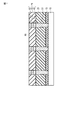
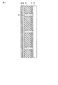
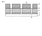
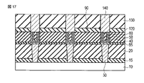
図1は、第1の実施形態に従った半導体装置の構成を示す断面図である。尚、以下の図において、既出の図と対応する部分には既出の図と同一符号を付してあり、詳細な説明は省略する。
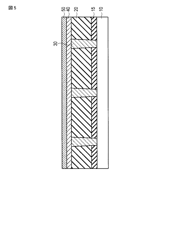
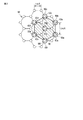
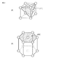
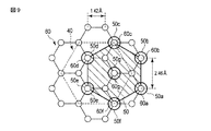
第1の実施形態では、助触媒層40が面心立方構造を有する場合には、助触媒層40は、その(111)面が半導体基板10の表面に対して平行になるように配向し、助触媒層40が六方最密構造を有する場合には、その(002)が半導体基板10の表面に対して平行になるように配向する。
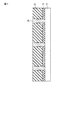
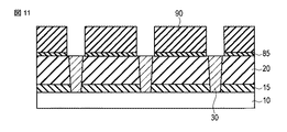
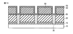
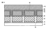
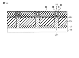
第1および第2の実施形態では、RIE法を用いて形成された配線(RIE配線)を具備する半導体装置について説明したが、本実施形態では、ダマシン法を用いて形成された配線(ダマシン配線)を具備する半導体装置について説明する。
Claims (8)
- 半導体基板と、
前記半導体基板の上方に設けられた配線とを具備し、
前記配線は、助触媒層と、前記助触媒層上に設けられた触媒層と、前記触媒層上に設けられたグラフェン層とを含み、
前記助触媒層のうち前記触媒層と接触している部分は、面心立方構造もしくは六方最密構造を有し、かつ、前記面心立方構造の(111)面もしくは前記六方最密構造の(002)面が前記半導体基板の表面と平行になるように配向しているか、または、前記助触媒層のうち前記触媒層と接触している部分は、アモルファス構造もしくは微結晶構造を有し、
前記触媒層は、面心立方構造もしくは六方最密構造を有し、かつ、前記面心立方構造の(111)面もしくは前記六方最密構造の(002)面が前記半導体基板の表面と平行になるように配向することを特徴とする半導体装置。 - 前記助触媒層のうち前記触媒層と接触している部分が、前記面心立方構造もしくは六方最密構造を有する場合、
前記助触媒層は、Ti、Cu、Zn、Zr、Ru、Rh、Pd、Ag、Hf、Re、Ir、PtおよびAuからなるグループのいずれかの材料からなる単層膜、前記グループのいずれかの材料の窒化物からなる単層膜、前記グループの中から選択される少なくとも二つの材料を含む合金からなる単層膜、または、Ti、Cu、Zn、Zr、Ru、Rh、Pd、Ag、Hf、Re、Ir、Pt、Au、前記複数の金属のそれぞれの窒化物、および、前記複数の金属の任意の二つ以上の金属からなる、前記複数の金属に関しての全ての合金からなるグループの中から選択される材料を二つ以上含む積層膜であることを特徴とする請求項1に記載の半導体装置。 - 前記助触媒層のうち前記触媒層と接触している部分が、前記アモルファス構造もしくは微結晶構造を有する場合、
前記助触媒層は、V、Cr、Mn、Nb、Mo、TaおよびWからなるグループのいずれかの材料からなる単層膜、前記グループのいずれかの材料の窒化物からなる単層膜、前記グループの中から選択される少なくとも二つの材料を含む合金からなる単層膜、または、V、Cr、Mn、Nb、Mo、Ta、W、前記複数の金属のそれぞれの窒化物、および、前記複数の金属の任意の二つ以上の金属からなる、前記複数の金属に関しての全ての合金からなるグループの中から選択される材料を二つ以上含む積層膜であることを特徴とする請求項1に記載の半導体装置。 - 前記触媒層は、Ni、CoおよびFeからなるグループのいずれかの材料からなる単層膜、前記グループのいずれかの材料の窒化物からなる単層膜、前記グループの中から選択される少なくとも二つの材料を含む合金からなる単層膜、または、Ni、Co、Fe、前記複数の金属のそれぞれの窒化物、および、前記複数の金属の任意の二つ以上の金属からなる、前記複数の金属に関しての全ての合金からなるグループの中から選択される材料を二つ以上含む積層膜であることを特徴とする請求項1ないし3のいずれか1項に記載の半導体装置。
- 半導体基板の表面の上方に、面心立方構造もしくは六方最密構造、または、アモルファス構造もしくは微結晶構造を有する、助触媒層を形成すること、前記助触媒層が前記面心立方構造もしくは前記六方最密構造を有するときは、前記面心立方構造の(111)面もしくは前記六方最密構造の(002)面が前記半導体基板の前記表面と平行に配向するように前記助触媒層を形成すること、
前記助触媒層上に、面心立方構造もしくは六方最密構造を有する触媒層を形成すること、前記触媒層が前記面心立方構造もしくは前記六方最密構造を有するときは、前記面心立方構造の(111)面もしくは前記六方最密構造の(002)面が前記半導体基板の前記表面と平行に配向するように前記触媒層を形成すること、前記助触媒層のうち前記触媒層と接触している部分は、前記面心立方構造もしくは前記六方最密構造、または、前記アモルファス構造もしくは前記微結晶構造であること、および、
前記触媒層上にグラフェン層を形成することを具備する半導体装置の製造方法。 - 前記助触媒層のうち前記触媒層と接触している部分が、前記面心立方構造もしくは六方最密構造を有する場合、
前記助触媒層は、Ti、Cu、Zn、Zr、Ru、Rh、Pd、Ag、Hf、Re、Ir、PtおよびAuからなるグループのいずれかの材料からなる単層膜、前記グループのいずれかの材料の窒化物からなる単層膜、前記グループの中から選択される少なくとも二つの材料を含む合金からなる単層膜、または、Ti、Cu、Zn、Zr、Ru、Rh、Pd、Ag、Hf、Re、Ir、Pt、Au、前記複数の金属のそれぞれの窒化物、および、前記複数の金属の任意の二つ以上の金属からなる、前記複数の金属に関しての全ての合金からなるグループの中から選択される材料を二つ以上含む積層膜であることを特徴とする請求項5に記載の半導体装置の製造方法。 - 前記助触媒層のうち前記触媒層と接触している部分が、前記アモルファスもしくは微結晶の構造を有する場合、
前記助触媒層は、V、Cr、Mn、Nb、Mo、TaおよびWからなるグループのいずれかの材料からなる単層膜、前記グループのいずれかの材料の窒化物からなる単層膜、前記グループの中から選択される少なくとも二つの材料を含む合金からなる単層膜、または、V、Cr、Mn、Nb、Mo、Ta、W、前記複数の金属のそれぞれの窒化物、および、前記複数の金属の任意の二つ以上の金属からなる、前記複数の金属に関しての全ての合金からなるグループの中から選択される材料を二つ以上含む積層膜であることを特徴とする請求項5に記載の半導体装置の製造方法。 - 前記触媒層は、Ni、CoおよびFeからなるグループのいずれかの材料からなる単層膜、前記グループのいずれかの材料の窒化物からなる単層膜、前記グループの中から選択される少なくとも二つの材料を含む合金からなる単層膜、または、Ni、Co、Fe、前記複数の金属のそれぞれの窒化物、および、前記複数の金属の任意の二つ以上の金属からなる、前記複数の金属に関しての全ての合金からなるグループの中から選択される材料を二つ以上含む積層膜であることを特徴とする請求項5ないし7のいずれか1項に記載の半導体装置の製造方法。
Priority Applications (1)
| Application Number | Priority Date | Filing Date | Title |
|---|---|---|---|
| JP2012036376A JP2012199520A (ja) | 2011-03-10 | 2012-02-22 | 半導体装置およびその製造方法 |
Applications Claiming Priority (3)
| Application Number | Priority Date | Filing Date | Title |
|---|---|---|---|
| JP2011052863 | 2011-03-10 | ||
| JP2011052863 | 2011-03-10 | ||
| JP2012036376A JP2012199520A (ja) | 2011-03-10 | 2012-02-22 | 半導体装置およびその製造方法 |
Publications (1)
| Publication Number | Publication Date |
|---|---|
| JP2012199520A true JP2012199520A (ja) | 2012-10-18 |
Family
ID=46794716
Family Applications (1)
| Application Number | Title | Priority Date | Filing Date |
|---|---|---|---|
| JP2012036376A Pending JP2012199520A (ja) | 2011-03-10 | 2012-02-22 | 半導体装置およびその製造方法 |
Country Status (2)
| Country | Link |
|---|---|
| US (1) | US8648464B2 (ja) |
| JP (1) | JP2012199520A (ja) |
Cited By (6)
| Publication number | Priority date | Publication date | Assignee | Title |
|---|---|---|---|---|
| JP2014187307A (ja) * | 2013-03-25 | 2014-10-02 | Toshiba Corp | 半導体装置及びその製造方法 |
| JP2015185599A (ja) * | 2014-03-20 | 2015-10-22 | 株式会社東芝 | グラフェン配線及び半導体装置 |
| US9659870B2 (en) | 2014-09-18 | 2017-05-23 | Kabushiki Kaisha Toshiba | Wiring and method for manufacturing the same |
| US9761530B2 (en) | 2014-09-18 | 2017-09-12 | Kabushiki Kaisha Toshiba | Graphene wiring and method for manufacturing the same |
| JP2020155471A (ja) * | 2019-03-18 | 2020-09-24 | 東京エレクトロン株式会社 | 半導体装置およびその製造方法 |
| WO2026023216A1 (ja) * | 2024-07-23 | 2026-01-29 | パナソニックホールディングス株式会社 | 半導体デバイスおよびその製造方法 |
Families Citing this family (16)
| Publication number | Priority date | Publication date | Assignee | Title |
|---|---|---|---|---|
| JP5591784B2 (ja) | 2011-11-25 | 2014-09-17 | 株式会社東芝 | 配線及び半導体装置 |
| US9202945B2 (en) * | 2011-12-23 | 2015-12-01 | Nokia Technologies Oy | Graphene-based MIM diode and associated methods |
| JP5668009B2 (ja) | 2012-03-26 | 2015-02-12 | 株式会社東芝 | 配線及び半導体装置 |
| US9472450B2 (en) * | 2012-05-10 | 2016-10-18 | Samsung Electronics Co., Ltd. | Graphene cap for copper interconnect structures |
| US9293412B2 (en) | 2012-12-17 | 2016-03-22 | International Business Machines Corporation | Graphene and metal interconnects with reduced contact resistance |
| US9437425B2 (en) * | 2013-01-11 | 2016-09-06 | Solan, LLC | Methods for integrating lead and graphene growth and devices formed therefrom |
| JP5813678B2 (ja) | 2013-02-15 | 2015-11-17 | 株式会社東芝 | 半導体装置 |
| WO2015126139A1 (en) | 2014-02-19 | 2015-08-27 | Samsung Electronics Co., Ltd. | Wiring structure and electronic device employing the same |
| KR102402545B1 (ko) * | 2014-02-19 | 2022-05-27 | 삼성전자주식회사 | 배선 구조 및 이를 적용한 전자소자 |
| JP6129772B2 (ja) * | 2014-03-14 | 2017-05-17 | 株式会社東芝 | 半導体装置及び半導体装置の製造方法 |
| JP6317232B2 (ja) * | 2014-10-29 | 2018-04-25 | 東京エレクトロン株式会社 | 選択成長方法および基板処理装置 |
| US9412654B1 (en) * | 2015-04-27 | 2016-08-09 | International Business Machines Corporation | Graphene sacrificial deposition layer on beol copper liner-seed for mitigating queue-time issues between liner and plating step |
| JP2017050419A (ja) | 2015-09-02 | 2017-03-09 | 株式会社東芝 | 半導体装置とその製造方法 |
| JP2017050503A (ja) * | 2015-09-04 | 2017-03-09 | 株式会社東芝 | 半導体装置とその製造方法 |
| CN112164697B (zh) * | 2020-09-28 | 2021-12-17 | 长江存储科技有限责任公司 | 一种半导体器件的制备方法、半导体结构 |
| US20240088042A1 (en) * | 2022-09-08 | 2024-03-14 | Taiwan Semiconductor Manufacturing Company Ltd. | Semiconductor structures and manufacturing method thereof |
Citations (9)
| Publication number | Priority date | Publication date | Assignee | Title |
|---|---|---|---|---|
| JPH04256313A (ja) * | 1991-02-08 | 1992-09-11 | Toshiba Corp | 半導体装置の製造方法 |
| JPH0794515A (ja) * | 1993-09-24 | 1995-04-07 | Texas Instr Japan Ltd | 積層膜、その形成方法及び半導体装置 |
| JPH09172077A (ja) * | 1995-12-20 | 1997-06-30 | Sony Corp | 半導体装置及びその製造方法 |
| JP2000183064A (ja) * | 1998-12-16 | 2000-06-30 | Matsushita Electronics Industry Corp | 半導体装置およびその製造方法 |
| JP2005332878A (ja) * | 2004-05-18 | 2005-12-02 | Seiko Epson Corp | 半導体装置の製造方法及び半導体装置 |
| JP2009070911A (ja) * | 2007-09-11 | 2009-04-02 | Fujitsu Ltd | 配線構造体、半導体装置および配線構造体の製造方法 |
| JP2009164432A (ja) * | 2008-01-08 | 2009-07-23 | Fujitsu Ltd | 半導体装置の製造方法、半導体装置および配線構造体 |
| US20100021708A1 (en) * | 2008-04-14 | 2010-01-28 | Massachusetts Institute Of Technology | Large-Area Single- and Few-Layer Graphene on Arbitrary Substrates |
| JP2011023420A (ja) * | 2009-07-13 | 2011-02-03 | Toshiba Corp | 半導体装置 |
Family Cites Families (6)
| Publication number | Priority date | Publication date | Assignee | Title |
|---|---|---|---|---|
| US8236118B2 (en) * | 2009-08-07 | 2012-08-07 | Guardian Industries Corp. | Debonding and transfer techniques for hetero-epitaxially grown graphene, and products including the same |
| KR101636442B1 (ko) * | 2009-11-10 | 2016-07-21 | 삼성전자주식회사 | 촉매합금을 이용한 그라핀의 제조방법 |
| JP2012041581A (ja) * | 2010-08-17 | 2012-03-01 | Sony Corp | コアシェル型微粒子及びこれを用いた機能デバイス |
| JP5150690B2 (ja) * | 2010-09-16 | 2013-02-20 | 株式会社東芝 | 半導体装置及び半導体装置の製造方法 |
| JP5550515B2 (ja) * | 2010-10-05 | 2014-07-16 | 株式会社東芝 | グラフェン配線およびその製造方法 |
| JP5637795B2 (ja) * | 2010-10-05 | 2014-12-10 | 株式会社東芝 | 装置 |
-
2012
- 2012-02-22 JP JP2012036376A patent/JP2012199520A/ja active Pending
- 2012-03-07 US US13/413,854 patent/US8648464B2/en active Active
Patent Citations (9)
| Publication number | Priority date | Publication date | Assignee | Title |
|---|---|---|---|---|
| JPH04256313A (ja) * | 1991-02-08 | 1992-09-11 | Toshiba Corp | 半導体装置の製造方法 |
| JPH0794515A (ja) * | 1993-09-24 | 1995-04-07 | Texas Instr Japan Ltd | 積層膜、その形成方法及び半導体装置 |
| JPH09172077A (ja) * | 1995-12-20 | 1997-06-30 | Sony Corp | 半導体装置及びその製造方法 |
| JP2000183064A (ja) * | 1998-12-16 | 2000-06-30 | Matsushita Electronics Industry Corp | 半導体装置およびその製造方法 |
| JP2005332878A (ja) * | 2004-05-18 | 2005-12-02 | Seiko Epson Corp | 半導体装置の製造方法及び半導体装置 |
| JP2009070911A (ja) * | 2007-09-11 | 2009-04-02 | Fujitsu Ltd | 配線構造体、半導体装置および配線構造体の製造方法 |
| JP2009164432A (ja) * | 2008-01-08 | 2009-07-23 | Fujitsu Ltd | 半導体装置の製造方法、半導体装置および配線構造体 |
| US20100021708A1 (en) * | 2008-04-14 | 2010-01-28 | Massachusetts Institute Of Technology | Large-Area Single- and Few-Layer Graphene on Arbitrary Substrates |
| JP2011023420A (ja) * | 2009-07-13 | 2011-02-03 | Toshiba Corp | 半導体装置 |
Cited By (7)
| Publication number | Priority date | Publication date | Assignee | Title |
|---|---|---|---|---|
| JP2014187307A (ja) * | 2013-03-25 | 2014-10-02 | Toshiba Corp | 半導体装置及びその製造方法 |
| JP2015185599A (ja) * | 2014-03-20 | 2015-10-22 | 株式会社東芝 | グラフェン配線及び半導体装置 |
| US9659870B2 (en) | 2014-09-18 | 2017-05-23 | Kabushiki Kaisha Toshiba | Wiring and method for manufacturing the same |
| US9761530B2 (en) | 2014-09-18 | 2017-09-12 | Kabushiki Kaisha Toshiba | Graphene wiring and method for manufacturing the same |
| JP2020155471A (ja) * | 2019-03-18 | 2020-09-24 | 東京エレクトロン株式会社 | 半導体装置およびその製造方法 |
| JP7304721B2 (ja) | 2019-03-18 | 2023-07-07 | 東京エレクトロン株式会社 | 半導体装置およびその製造方法 |
| WO2026023216A1 (ja) * | 2024-07-23 | 2026-01-29 | パナソニックホールディングス株式会社 | 半導体デバイスおよびその製造方法 |
Also Published As
| Publication number | Publication date |
|---|---|
| US20120228614A1 (en) | 2012-09-13 |
| US8648464B2 (en) | 2014-02-11 |
Similar Documents
| Publication | Publication Date | Title |
|---|---|---|
| JP5801221B2 (ja) | 半導体装置の製造方法および半導体装置 | |
| JP2012199520A (ja) | 半導体装置およびその製造方法 | |
| US10971451B2 (en) | Interconnect structure having nanocrystalline graphene cap layer and electronic device including the interconnect structure | |
| JP5826783B2 (ja) | 半導体装置 | |
| US9117885B2 (en) | Graphene interconnection and method of manufacturing the same | |
| US8487449B2 (en) | Carbon nanotube interconnection and manufacturing method thereof | |
| US8309407B2 (en) | Electronic devices including carbon-based films having sidewall liners, and methods of forming such devices | |
| US9159615B2 (en) | Graphene interconnection and method of manufacturing the same | |
| US10978342B2 (en) | Interconnect with self-forming wrap-all-around barrier layer | |
| US9443805B2 (en) | Wire and semiconductor device | |
| US20130252417A1 (en) | Thin film forming method | |
| JP2022504926A (ja) | ビット線抵抗低減のためのキャップ層 | |
| US20160071803A1 (en) | Semiconductor device and method for manufacturing the same | |
| US9392690B2 (en) | Method and structure to improve the conductivity of narrow copper filled vias | |
| JP7810447B2 (ja) | Cmos適合グラフェン構造、インターコネクト及びその製造方法 | |
| CN114121782A (zh) | 形成互连结构的方法 | |
| US11217531B2 (en) | Interconnect structure having nanocrystalline graphene cap layer and electronic device including the interconnect structure | |
| TWI495059B (zh) | 半導體元件與半導體裝置與其形成方法 | |
| JP5384269B2 (ja) | Cu配線の形成方法 | |
| KR20160124958A (ko) | 반도체 소자 및 그 제조 방법 | |
| US9484206B2 (en) | Semiconductor device including catalyst layer and graphene layer thereon and method for manufacturing the same | |
| US12400975B2 (en) | Interconnect structure and electronic device including the same | |
| US20140284814A1 (en) | Semiconductor device and manufacturing method thereof | |
| JP2026071248A (ja) | Cmos適合グラフェン構造、インターコネクト及びその製造方法 | |
| FR3061356A1 (fr) | Substrat pour le depot d'un film de graphene |
Legal Events
| Date | Code | Title | Description |
|---|---|---|---|
| RD04 | Notification of resignation of power of attorney |
Free format text: JAPANESE INTERMEDIATE CODE: A7424 Effective date: 20131205 |
|
| RD04 | Notification of resignation of power of attorney |
Free format text: JAPANESE INTERMEDIATE CODE: A7424 Effective date: 20131212 |
|
| RD04 | Notification of resignation of power of attorney |
Free format text: JAPANESE INTERMEDIATE CODE: A7424 Effective date: 20131219 |
|
| RD04 | Notification of resignation of power of attorney |
Free format text: JAPANESE INTERMEDIATE CODE: A7424 Effective date: 20131226 |
|
| RD04 | Notification of resignation of power of attorney |
Free format text: JAPANESE INTERMEDIATE CODE: A7424 Effective date: 20140109 |
|
| A621 | Written request for application examination |
Free format text: JAPANESE INTERMEDIATE CODE: A621 Effective date: 20140207 |
|
| A977 | Report on retrieval |
Free format text: JAPANESE INTERMEDIATE CODE: A971007 Effective date: 20141009 |
|
| A131 | Notification of reasons for refusal |
Free format text: JAPANESE INTERMEDIATE CODE: A131 Effective date: 20141014 |
|
| A02 | Decision of refusal |
Free format text: JAPANESE INTERMEDIATE CODE: A02 Effective date: 20150224 |