JP2012199633A - Imaging element and imaging apparatus provided with the same - Google Patents
Imaging element and imaging apparatus provided with the same Download PDFInfo
- Publication number
- JP2012199633A JP2012199633A JP2011060836A JP2011060836A JP2012199633A JP 2012199633 A JP2012199633 A JP 2012199633A JP 2011060836 A JP2011060836 A JP 2011060836A JP 2011060836 A JP2011060836 A JP 2011060836A JP 2012199633 A JP2012199633 A JP 2012199633A
- Authority
- JP
- Japan
- Prior art keywords
- light
- microlens
- light receiving
- imaging
- incident
- Prior art date
- Legal status (The legal status is an assumption and is not a legal conclusion. Google has not performed a legal analysis and makes no representation as to the accuracy of the status listed.)
- Withdrawn
Links
Images


Landscapes
- Lenses (AREA)
- Testing, Inspecting, Measuring Of Stereoscopic Televisions And Televisions (AREA)
- Studio Devices (AREA)
- Cameras In General (AREA)
- Stereoscopic And Panoramic Photography (AREA)
Abstract
【課題】小型、低価格で、撮像光学系のアライメント作業が容易な3D画像撮像用の撮像装置を提供する。
【解決手段】撮像装置は、物体面からの光が集光される3D画像撮像用の撮像素子を備える。撮像素子は、マイクロレンズアレイ51を有すると共に、該マイクロレンズアレイ51のマイクロレンズ51aそれぞれに対し少なくとも一対の受光部52L,52Rを有し、マイクロレンズアレイ51に右側から入射した光BRを、受光部52Lで受光し、マイクロレンズアレイ51に左側から入射した光BLを、受光部52Rで受光する。
【選択図】図2An image pickup apparatus for 3D image pickup that is small in size and low in price and easy in alignment work of an image pickup optical system is provided.
An imaging apparatus includes an imaging element for 3D image imaging in which light from an object surface is collected. The imaging device has a microlens array 51 and at least a pair of light receiving portions 52L and 52R for each of the microlenses 51a of the microlens array 51, and receives light BR incident on the microlens array 51 from the right side. The light BL received by the unit 52L and incident on the microlens array 51 from the left side is received by the light receiving unit 52R.
[Selection] Figure 2
Description
本発明は、3D表示用の視差のある画像を撮像する撮像素子及び該撮像素子を備えた撮像装置に関するものである。 The present invention relates to an imaging device that captures an image with parallax for 3D display, and an imaging device including the imaging device.
3D方式は、一般に撮像光学系と撮像素子で構成される2つのカメラを左右方向に配置して視差の異なる2つの画像(右画像と左画像)を撮影し、その右画像、左画像を、3Dテレビや3Dディスプレイに表示し、偏光方式やタイムフィールドシーケンシャル方式の眼鏡を用いて、それぞれ右画像を右眼、左画像を左眼のみに見えるようにすることで、脳の中で映像が合成され立体感を得ている。 The 3D method generally arranges two cameras composed of an imaging optical system and an imaging element in the left-right direction to photograph two images (right image and left image) with different parallaxes, and the right image and the left image are Displayed on a 3D TV or 3D display, and using polarized or time field sequential glasses, the right image can be seen only by the left eye and the left image can be seen only by the left eye, thereby synthesizing the video in the brain. It has a three-dimensional effect.
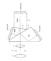
3D画像表示用に視差の異なる2つの画像を撮像する方法として、上述とは異なり、1つの撮像光学系で取り込んだ物体光を撮像光学系で2つに分割する方法がある(例えば特許文献1)。図9(A)は、特許文献1に開示の3D表示用の撮像装置を説明する図で、図9(B)は図9(A)の3D用撮像装置の絞り102のA方向矢視図である。
As a method for capturing two images with different parallaxes for 3D image display, unlike the above, there is a method in which object light captured by one imaging optical system is divided into two by the imaging optical system (for example, Patent Document 1). ). 9A is a diagram for explaining the 3D display imaging device disclosed in Patent Document 1, and FIG. 9B is a view in the direction of the arrow A of the
特許文献1の撮像光学系では、図9(A)に示すように、物体面(図示せず)の1点から撮像光学系内の1次光学系101に入射する光束の内、図の右側を進行する光BRは撮像光学系の絞り102の右側102Rに到達する。同様に図の左側を進行する光BLは撮像光学系の絞り102の左側102Lに到達する。図示した光軸上の物体光だけでなく、軸外のものについても同様である(例えば、主光線方向に対し右側を進行する光は撮像光学系の絞り102の右側102Rに到達する)。すなわち、図9(B)に示すように、撮像光学系の絞り102を左側領域102aと右側領域102bに分割すると、左側領域102aには物体から左方向に向かう光束が、右側領域102bには物体から右方向に向かう光束が集まるため、左側領域102aと左側領域102bとでは、視差の異なる光が集まる。
In the imaging optical system of Patent Document 1, as shown in FIG. 9A, the right side of the figure among the light beams incident on the primary
絞り102の左側領域102aを通過した光は、プリズム103により左側に反射され、さらに反射ミラー104aにより反射され、結像レンズ105aを透過し、撮像素子106aにより受光される。一方、絞り102の右側領域102bを通過した光は、プリズム103により右側に反射され、さらに反射ミラー104bにより反射され、結像レンズ105bを透過し、撮像素子106aとは別の撮像素子106bにより受光される。このようにして、視差の異なる二つの画像を撮像するようにしている。
The light that has passed through the
しかしながら、特許文献1に開示の3D表示用の撮像装置では、視差の異なる2つの画像を2つの撮像素子より得ており、プリズムで分離した後の撮像素子に結像するための2次光学系が2つ必要となる。そのため、撮像光学系全体が大型化すると同時に複雑な光学系が必要となる。また、光学研磨した高精度なプリズムの単価も高く、部品数も多いため製造コストが高い。更にプリズム、2次光学系、撮像素子などの光軸の高精度なアライメント作業が必要となるため生産性が低い。 However, in the imaging device for 3D display disclosed in Patent Document 1, two images having different parallax are obtained from two imaging elements, and a secondary optical system for forming an image on the imaging element after being separated by a prism. Two are required. For this reason, the entire imaging optical system is enlarged, and at the same time, a complicated optical system is required. Moreover, the unit cost of the optically polished high-accuracy prism is high, and the manufacturing cost is high due to the large number of parts. Furthermore, since high-precision alignment work of optical axes such as a prism, a secondary optical system, and an image sensor is required, productivity is low.
本発明は、かかる事情に鑑みてなされたものであり、3D表示用の撮像装置の小型化、低コスト化が可能で、撮像光学系のアライメント作業が容易な3D表示用の撮像素子及び該撮像素子を備えた撮像装置を提供することを目的とする。 The present invention has been made in view of such circumstances, and an image pickup device for 3D display that can reduce the size and cost of an image pickup device for 3D display and that can easily perform an alignment operation of an image pickup optical system, and the image pickup. An object of the present invention is to provide an imaging device including an element.
上記課題を解決するために、本発明の第1の技術手段は、物体面からの光が集光される3D画像撮像用の撮像素子であって、マイクロレンズアレイを有すると共に、該マイクロレンズアレイのマイクロレンズそれぞれに対し少なくとも一対の受光部を有し、所定の方向に関して一方の側から前記マイクロレンズアレイに入射した光を、前記一対の受光部の一方で受光し、前記所定の方向に関して他方の側から前記マイクロレンズアレイに入射した光を、前記一対の受光部の他方で受光することを特徴としたものである。 In order to solve the above-mentioned problems, a first technical means of the present invention is an image pickup device for 3D image pickup in which light from an object surface is collected, and has a microlens array, and the microlens array Each of the microlenses has at least a pair of light receiving portions, and receives light incident on the microlens array from one side with respect to a predetermined direction, and receives the light with one of the pair of light receiving portions and the other with respect to the predetermined direction. The light incident on the microlens array from the side is received by the other of the pair of light receiving portions.
本発明の第2の技術手段は、第1の技術手段において、前記マイクロレンズアレイが、マイクロレンズ毎に、前記所定の方向から前記マイクロレンズの入射面側に入射する光を集光するための凸部を有し、前記凸部が集光した光を少なくとも2方向に分離することにより前記一対の受光部の両方に導く、少なくとも2つの異なる角度の傾斜面を前記マイクロレンズの出射面側に有することを特徴としたものである。 According to a second technical means of the present invention, in the first technical means, the microlens array collects light incident on the incident surface side of the microlens from the predetermined direction for each microlens. An inclined surface having at least two different angles that guides both of the pair of light receiving portions by separating the light collected by the convex portion in at least two directions on the emission surface side of the microlens. It is characterized by having.
本発明の第3の技術手段は、第2の技術手段において、前記マイクロレンズの出射面側に配置された少なくとも2つの異なる角度の傾斜面の分割位置である頂部が、前記マイクロレンズの入射面側に配置された前記凸部の光軸上に位置することを特徴としたものである。 According to a third technical means of the present invention, in the second technical means, a top portion which is a division position of at least two different inclined surfaces arranged on the exit surface side of the microlens is an incident surface of the microlens. It is located on the optical axis of the said convex part arrange | positioned at the side.
本発明の第4の技術手段は、第3の技術手段において、前記マイクロレンズの出射面側に配置された少なくとも2つの異なる角度の傾斜面は、光の入射側に凸形状の曲面であることを特徴としたものである。 According to a fourth technical means of the present invention, in the third technical means, the inclined surfaces of at least two different angles arranged on the exit surface side of the microlens are convex curved surfaces on the light incident side. It is characterized by.
本発明の第5の技術手段は、第3の技術手段において、前記マイクロレンズの出射面側に配置された少なくとも2つの異なる角度の傾斜面は、光の入射側に凹形状の曲面であることを特徴としたものである。 According to a fifth technical means of the present invention, in the third technical means, the inclined surfaces of at least two different angles arranged on the exit surface side of the microlens are concave curved surfaces on the light incident side. It is characterized by.
本発明の第6の技術手段は、第1〜5のいずれか1の技術手段の撮像素子と、物体面からの光を前記撮像素子に導光する光学系とを備える撮像装置である。 A sixth technical means of the present invention is an imaging apparatus comprising: the image sensor of any one of the first to fifth technical means; and an optical system that guides light from an object plane to the image sensor.
本発明によれば、小型、低価格で、撮像光学系のアライメント作業が容易な3D表示用の撮像装置を提供できる。 According to the present invention, it is possible to provide an image pickup apparatus for 3D display that is small in size and low in price and can easily perform an alignment operation of an image pickup optical system.
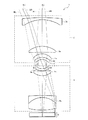
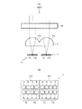
図1及び図2を用いて、本発明の3D表示用の撮像装置を説明する。図1は、本発明の撮像装置の主要部の構成を示す図、図2は、図1の撮像装置の撮像素子の構成を示す図である。
本発明の3D画像撮像用の撮像装置は、図1の参照符号1で例示するように、1次光学系2と、絞り3と、2次光学系4と、撮像素子5と、を備える。
1次光学系2は、レンズ2a〜2dより構成されるものであって、物体面(図示せず)上の1点からの光束を絞り3に集光する。
2次光学系4は、レンズ4a〜4cより構成されるものであって、1次光学系2により絞り3により絞られた光を、撮像素子5に結像させる。また本実施例では、本撮像光学系は絞り3の中央を通る主光線が撮像素子5に垂直に入射する、いわゆる像側テレセントリック光学系としている。
The image pickup apparatus for 3D display according to the present invention will be described with reference to FIGS. 1 and 2. FIG. 1 is a diagram illustrating a configuration of a main part of an imaging apparatus according to the present invention, and FIG. 2 is a diagram illustrating a configuration of an imaging element of the imaging apparatus in FIG.
The image pickup apparatus for 3D image pickup according to the present invention includes a primary optical system 2, a diaphragm 3, a secondary optical system 4, and an image sensor 5 as illustrated by reference numeral 1 in FIG. 1.
The primary optical system 2 is composed of
The secondary optical system 4 is composed of
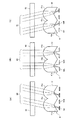
撮像素子5は、1次光学系、2次光学系より構成される撮像光学系の焦点位置近傍に配置され、図2に示すように、正のパワーを有する凸形状のマイクロレンズ51aが光の入射面側に形成されたマイクロレンズアレイ51と、各マイクロレンズ51aの焦点面近傍に1つのマイクロレンズ51aに対して一対の受光部52L、52Rを有する受光素子52と、これらマイクロレンズアレイ51及び受光素子52を保護するためのカバーガラス53を有する。
The imaging element 5 is disposed in the vicinity of the focal position of an imaging optical system composed of a primary optical system and a secondary optical system. As shown in FIG. 2, a
図1及び図2(B)に示すように、3D用撮像装置1では、物体面(図示せず)上の1点から当該装置1に入射する光束のうち、絞り3の絞り面の中央を通過する主光線BCは、所定の方向から(本例では垂直方向から)撮像素子5に入射するが、この主光線BCは、撮像素子5の受光素子52の受光部52Lと受光部52Rの境目に入射する。
図1及び図2(A)に示すように、3D用撮像装置1において、上記光束のうち、主光線BCより右側に向けて発せられた光BRは、絞り3の絞り面の右側に到達し、撮像素子5に対して右側から角度を持って入射し、当該素子5の受光素子52の左側の受光部52Lに入射する。
また、図1及び図2(C)に示すように、3D用撮像装置1において、上記光束のうち、上記光BRと視差の異なる、主光線BCより左側に向けて発せられた光BLは、絞り3の絞り面の左側に到達し、撮像素子5に対して左側から角度をもって入射し、当該素子5の受光素子52の右側の受光部52Rに入射する。
そして、3D用撮像装置1では、受光素子5の左側の受光部52Lで得られた画像と、右側の受光部52Rで得られた画像とを別の画像として処理し、立体表示用の視差のある2つの画像を生成している。
As shown in FIGS. 1 and 2B, in the 3D imaging apparatus 1, the center of the diaphragm surface of the diaphragm 3 out of the light flux incident on the apparatus 1 from one point on the object plane (not shown). The principal ray BC passing through is incident on the image sensor 5 from a predetermined direction (in this example, from the vertical direction), and this principal ray BC is a boundary between the
As shown in FIGS. 1 and 2A, in the 3D imaging apparatus 1, the light BR emitted toward the right side of the principal ray BC out of the light flux reaches the right side of the stop surface of the stop 3. Then, the light enters the imaging element 5 at an angle from the right side, and enters the light
In addition, as shown in FIGS. 1 and 2C, in the 3D imaging apparatus 1, the light BL emitted from the principal beam BC to the left side, which has a parallax different from the light BR, out of the luminous flux is It reaches the left side of the diaphragm surface of the diaphragm 3, enters the imaging element 5 with an angle from the left side, and enters the
In the 3D imaging device 1, the image obtained by the left
この3D用撮像装置1は、視差の異なる2つの画像を生成するのに撮像素子を1つしか使用しないため、低コストとすることができる。また、必要な撮像光学系は1つであるため、光軸の高精度のアライメント作業が容易となり生産性が高く、装置を小型化することもでき、更に低コストとすることができる。さらに、特許文献1に開示の装置で用いていた光学研磨した高精度なプリズムも不要であるので、コストを抑えることができる。
なお、3D用撮像装置1は、2D表示用に用いることもでき、この場合は、左側の受光部52Lでの画素値と右側の受光部52Rでの画素値の和を1つの画素値とすることが好ましい。撮像素子の感度特性が向上できるためである。
Since the 3D imaging apparatus 1 uses only one imaging element to generate two images having different parallaxes, the cost can be reduced. In addition, since only one imaging optical system is required, high-precision alignment work of the optical axis is facilitated, the productivity is high, the apparatus can be miniaturized, and the cost can be further reduced. Furthermore, since the optically polished high-precision prism used in the apparatus disclosed in Patent Document 1 is not necessary, the cost can be reduced.
The 3D imaging device 1 can also be used for 2D display. In this case, the sum of the pixel value in the left
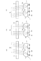
図3は、撮像素子の他の例を示す図である。図2と同様の部分については、同じ参照符号を付すことにより、その説明を省略する。
図3の撮像素子6は、図2の撮像素子5と同様に、図3(A)に示すように、正のパワーを有する凸形状のマイクロレンズ51aがマイクロレンズアレイ61の入射面側に形成されており、撮像素子6に対して右側から角度を持って入射した光BRが、受光素子52の左側の受光部52Lに入射し、図3(C)に示すように、撮像素子6に対して左側から角度をもって入射した光BLが、受光素子52の右側の受光部52Rに入射する。
FIG. 3 is a diagram illustrating another example of the imaging element. The same parts as those in FIG. 2 are denoted by the same reference numerals, and the description thereof is omitted.
3, a
しかし、撮像素子6は、図2の撮像素子5とは異なり、マイクロレンズアレイ61の出射面側に1対の2つの異なる角度のプリズム形状の傾斜面61aを有し、図3(B)に示すように、撮像素子6に対して略垂直に入射した光BCが、撮像素子6の受光素子52の受光部52L,52Rにも入射するようになっている。
図2の例では、絞りの絞り面の中央すなわち瞳の中心を通過し撮像素子に垂直で入射する光BCは、撮像素子5の受光部で受光できずロスとなっていたが、本例では受光できるため、光のロスを減らすことができる。また図2の例では撮像素子の画素の間隔が小さくなり高い半導体の製造プロセスルールの製造装置の精度が必要となるが、図3の例では撮像素子の製造プロセス上も有利となる。
なお、受光部52Lと受光部52Rの位置がマイクロレンズ51aの光軸に関して対称である場合、2つの異なる角度の傾斜面61aの分割位置すなわち傾斜面61aの頂部は、マイクロレンズ51aの光軸上とするのがよい。撮像素子6に対して垂直に入射した光BCを、受光部52Lと受光部52Rとで均等に受光できる。
However, unlike the image pickup device 5 of FIG. 2, the image pickup device 6 has a pair of two prism-shaped
In the example of FIG. 2, the light BC that passes through the center of the stop surface of the diaphragm, that is, the center of the pupil and is perpendicularly incident on the image sensor cannot be received by the light receiving unit of the image sensor 5, but is lost. Since light can be received, loss of light can be reduced. Further, in the example of FIG. 2, the interval between the pixels of the image sensor becomes small and the high manufacturing accuracy of the semiconductor manufacturing process rule is required, but the example of FIG. 3 is also advantageous in the process of manufacturing the image sensor.
When the positions of the
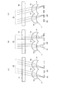
図4は、撮像素子の別の例を示す図である。図3と同様の部分については、同じ参照符号を付すことにより、その説明を省略する。
図4の撮像素子7は、図3の撮像素子6と同様に、図4(A)に示すように、マイクロレンズ51aがマイクロレンズアレイ71の入射面側に形成されており、撮像素子7に対して右側から角度を持って入射した光BRが、受光素子52の左側の受光部52Lに入射し、図4(C)に示すように、撮像素子7に対して左側から角度をもって入射した光BLが、受光素子52の右側の受光部52Rに入射する。また、撮像素子7は、マイクロレンズアレイ71の出射面側に1対の2つの異なる角度の傾斜面71aを有し、図4(B)に示すように、撮像素子7に対して略垂直に入射した光BCが、撮像素子7の受光素子52の受光部52L,52Rにも入射するようになっている。
しかし、撮像素子7は、図3の撮像素子6とは異なり、マイクロレンズアレイ71の出射面側に配置される1対の2つの異なる角度の傾斜面の端面が平面ではなく、光の入射側に凹の形状となっている。これにより、マイクロレンズ全体の焦点距離が短くなるため、集光径が小さくなり受光部52L,52Rへの集光性能を上げることが可能となる。
FIG. 4 is a diagram illustrating another example of the image sensor. The same parts as those in FIG. 3 are denoted by the same reference numerals, and the description thereof is omitted.
4 has a
However, unlike the image pickup element 6 of FIG. 3, the image pickup element 7 is not an end face of a pair of two inclined surfaces with different angles arranged on the exit surface side of the
図5は、撮像素子の別の例を示す図である。図3と同様の部分については、同じ参照符号を付すことにより、その説明を省略する。
図5の撮像素子8は、図3の撮像素子6と同様に、図5(A)に示すように、マイクロレンズ51aがマイクロレンズアレイ81の入射面側に形成されており、撮像素子7に対して右側から角度を持って入射した光BRが、受光素子52の左側の受光部52Lに入射し、図5(C)に示すように、撮像素子8に対して左側から角度をもって入射した光BLが、受光素子52の右側の受光部52Rに入射する。また、撮像素子7は、マイクロレンズアレイ81の出射面側に1対の2つの異なる角度の傾斜面81aを有し、図5(B)に示すように、撮像素子8に対して略垂直に入射した光BCが、撮像素子8の受光素子52の受光部52L,52Rにも入射するようになっている。
しかし、撮像素子8は、図3の撮像素子6とは異なり、マイクロレンズアレイ81の出射面側に配置される1対の2つの異なる角度の傾斜面端面が平面ではなく、光の入射側に凸の形状となっている。これにより、焦点距離を長くし、受光部52L,52Lまでの距離を長くすることができるので、受光部52Lと受光部52Rへの光の分離性を上げることができる。
なお、図4や図5の例のマイクロレンズアレイでは、出射面側の端面の形状を非球面形状とすることにより、平面形状とした場合より、出射面側での収差を低減することできる。
FIG. 5 is a diagram illustrating another example of the image sensor. The same parts as those in FIG. 3 are denoted by the same reference numerals, and the description thereof is omitted.
5, as with the image sensor 6 in FIG. 3, the
However, unlike the image sensor 6 of FIG. 3, the
In the microlens array of the example of FIGS. 4 and 5, the end surface on the exit surface side is aspherical, so that aberration on the exit surface side can be reduced as compared with a planar shape.
図6は、本発明の3D表示用のカラー撮像装置の主要部の構成を示す図である。図1と同様の部分については、同じ参照符号を付すことによりその説明を省略する。
図の3D用カラー撮像装置1´は、ダイクロイックミラー91,92による反射面を内部に備えた色分解プリズム9を有し、撮像光学系2,4を通過した光をRGBそれぞれ別の光路に色分解する。色分解されたRGBの光路に上述の撮像素子5(5R,5G,5B),6(6R,6G,6B),7(7R,7G,7B),8(8R,8G,8B)のいずれかを配置することにより、RGBの画像を撮像できるため、RGB画像を合成することにより、視差のある2つのRGB画像を撮像できる。
FIG. 6 is a diagram showing a configuration of a main part of the color imaging apparatus for 3D display according to the present invention. The same parts as those in FIG. 1 are denoted by the same reference numerals, and the description thereof is omitted.
The 3D color image pickup apparatus 1 ′ shown in the figure has a color separation prism 9 provided with reflection surfaces by
上述の例では、撮像素子の受光素子は、モノクロ用のものであったが、ベイヤ配列の受光素子に代表されるカラー用の受光素子を用いてもよい。
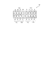
図7(A)は、ベイヤ配列の受光素子を用いた撮像素子の一例を示す図であり、図7(B)は、図7(A)のX方向矢視拡大図である。図8は、ベイヤ配列の受光素子を用いる場合のマイクロレンズアレイのレンズ形状の他の例を示す図である。
In the above example, the light receiving element of the imaging element is for monochrome, but a color light receiving element represented by a Bayer array of light receiving elements may be used.
FIG. 7A is a diagram illustrating an example of an image sensor using a Bayer array of light receiving elements, and FIG. 7B is an enlarged view in the direction of arrow X in FIG. 7A. FIG. 8 is a diagram showing another example of the lens shape of the microlens array in the case of using a Bayer array of light receiving elements.
図7の撮像素子10は、ベイヤ配列の撮像素子11を有する。ベイヤ配列の撮像素子は、4つのカラーフィルタ付の受光部から1画素の画像を作成するものが一般的である。したがって、この場合は1つのマイクロレンズ51aの中にRGGB4個の受光部を1セットの受光部として、2セットの受光部11L,11Rを配列すればよい。そして、撮像素子10に対して右側から角度を持って入射した光が、受光素子11の左側の受光部11Lに入射し、撮像素子10に対して左側から角度をもって入射した光が、受光素子11の右側の受光部11Rに入射するようにすればよい。またマイクロレンズの形状が、図3、図4、図5の形状のときにも、同様にベイヤ配列の撮像素子を使用することが可能である。
The
なお、図8に示すように、マイクロレンズアレイ51´のマイクロレンズ51a´の形状は、入射面に対して垂直方向から見て縦横非対称にしてもよい。これにより縦方向と横方向の受光部11L,11Rのピッチを同じにすることが可能となる。
As shown in FIG. 8, the shape of the
本発明では像側テレセントリックな撮像光学系で例を示したが、必ずしも像側テレセントリックにする必要はない。撮像光学系を小さくするためには中央から周辺に向かうに従い撮像素子への入射角度が大きくなるのが一般的であるが、この場合撮像素子の受光部に対してマイクロレンズの光軸をオフセットすることにより周辺の光量を確保することができる。このように像面の周辺の主光線が角度を有する場合でも対応は可能である。その場合は周辺のプリズム面の角度を主光線の傾き分傾斜させることにより、均等に右画像と左画像の光を分離することができる。 In the present invention, an example is shown with an image-side telecentric imaging optical system, but the image-side telecentric is not necessarily required. In order to reduce the imaging optical system, it is common that the incident angle to the imaging device increases as it goes from the center to the periphery. In this case, the optical axis of the microlens is offset with respect to the light receiving portion of the imaging device. Thus, the amount of light in the periphery can be secured. Thus, it is possible to cope with the case where the principal ray around the image plane has an angle. In that case, the light of the right image and the left image can be evenly separated by inclining the angle of the peripheral prism surface by the inclination of the principal ray.
1,1´…3D用撮像装置、2…1次光学系、3…絞り、4…2次光学系、5,6,7,8,10…撮像素子、51,51´,61,71,81…マイクロレンズアレイ、52,11…受光素子、61a,71a,81a…傾斜面、9…色分解プリズム。 DESCRIPTION OF SYMBOLS 1,1 '... 3D imaging device, 2 ... Primary optical system, 3 ... Diaphragm, 4 ... Secondary optical system, 5, 6, 7, 8, 10 ... Image sensor, 51, 51', 61, 71, 81: microlens array, 52, 11: light receiving element, 61a, 71a, 81a ... inclined surface, 9 ... color separation prism.
Claims (6)
マイクロレンズアレイを有すると共に、該マイクロレンズアレイのマイクロレンズそれぞれに対し少なくとも一対の受光部を有し、所定の方向に関して一方の側から前記マイクロレンズアレイに入射した光を、前記一対の受光部の一方で受光し、前記所定の方向に関して他方の側から前記マイクロレンズアレイに入射した光を、前記一対の受光部の他方で受光することを特徴とする撮像素子。 An image sensor for 3D image capturing in which light from an object surface is collected,
A microlens array and at least a pair of light receiving portions for each of the microlenses of the microlens array, and light incident on the microlens array from one side with respect to a predetermined direction. An image pickup device that receives light on one side and receives light incident on the microlens array from the other side with respect to the predetermined direction at the other of the pair of light receiving units.
Priority Applications (1)
| Application Number | Priority Date | Filing Date | Title |
|---|---|---|---|
| JP2011060836A JP2012199633A (en) | 2011-03-18 | 2011-03-18 | Imaging element and imaging apparatus provided with the same |
Applications Claiming Priority (1)
| Application Number | Priority Date | Filing Date | Title |
|---|---|---|---|
| JP2011060836A JP2012199633A (en) | 2011-03-18 | 2011-03-18 | Imaging element and imaging apparatus provided with the same |
Publications (1)
| Publication Number | Publication Date |
|---|---|
| JP2012199633A true JP2012199633A (en) | 2012-10-18 |
Family
ID=47181461
Family Applications (1)
| Application Number | Title | Priority Date | Filing Date |
|---|---|---|---|
| JP2011060836A Withdrawn JP2012199633A (en) | 2011-03-18 | 2011-03-18 | Imaging element and imaging apparatus provided with the same |
Country Status (1)
| Country | Link |
|---|---|
| JP (1) | JP2012199633A (en) |
Cited By (1)
| Publication number | Priority date | Publication date | Assignee | Title |
|---|---|---|---|---|
| CN105988150A (en) * | 2015-03-04 | 2016-10-05 | 奇景光电股份有限公司 | Lens module |
-
2011
- 2011-03-18 JP JP2011060836A patent/JP2012199633A/en not_active Withdrawn
Cited By (1)
| Publication number | Priority date | Publication date | Assignee | Title |
|---|---|---|---|---|
| CN105988150A (en) * | 2015-03-04 | 2016-10-05 | 奇景光电股份有限公司 | Lens module |
Similar Documents
| Publication | Publication Date | Title |
|---|---|---|
| US8456565B2 (en) | Imaging device | |
| KR101701527B1 (en) | Three-dimensional image capture device | |
| US9784984B2 (en) | Imaging apparatus and imaging method | |
| US9851483B2 (en) | Stereoscopic imaging method and system that divides a pixel matrix into subgroups | |
| US20160120397A1 (en) | Endoscope image-acquisition device | |
| JP2008294819A (en) | Imaging device | |
| CN102685377A (en) | Image pickup apparatus | |
| JP6217918B2 (en) | Array-like optical element, imaging member, imaging element, imaging device, and distance measuring device | |
| TWI461824B (en) | Stereo imaging device | |
| JP2012215720A (en) | Stereoscopic image pickup device and stereoscopic image pickup method | |
| US9110368B2 (en) | Anamorphic stereoscopic optical apparatus and related methods | |
| JP2012212978A (en) | Imaging element and imaging device | |
| JP7331222B2 (en) | Optical device and imaging device | |
| WO2011134215A1 (en) | Stereoscopic camera device | |
| JP2662252B2 (en) | 3D image display device | |
| CN105359519B (en) | Camera head | |
| JP2010249941A (en) | Stereo imaging device | |
| JP2002191060A (en) | Three-dimensional imaging unit | |
| JP2012199633A (en) | Imaging element and imaging apparatus provided with the same | |
| US7791667B2 (en) | Focus detection apparatus and image-pickup apparatus including the same | |
| US20240430553A1 (en) | Imaging apparatus | |
| JP2012220848A (en) | Imaging device and lens device | |
| JP4360180B2 (en) | 3D image shooting device | |
| JP2008180808A (en) | Stereoscopic imaging apparatus | |
| CN111258166A (en) | Camera module, periscopic camera module, image acquisition method and working method |
Legal Events
| Date | Code | Title | Description |
|---|---|---|---|
| A300 | Application deemed to be withdrawn because no request for examination was validly filed |
Free format text: JAPANESE INTERMEDIATE CODE: A300 Effective date: 20140603 |