JP2012209408A - Manufacturing method of electronic component and wiring board - Google Patents
Manufacturing method of electronic component and wiring board Download PDFInfo
- Publication number
- JP2012209408A JP2012209408A JP2011073573A JP2011073573A JP2012209408A JP 2012209408 A JP2012209408 A JP 2012209408A JP 2011073573 A JP2011073573 A JP 2011073573A JP 2011073573 A JP2011073573 A JP 2011073573A JP 2012209408 A JP2012209408 A JP 2012209408A
- Authority
- JP
- Japan
- Prior art keywords
- solder
- land
- electrode
- shape
- portions
- Prior art date
- Legal status (The legal status is an assumption and is not a legal conclusion. Google has not performed a legal analysis and makes no representation as to the accuracy of the status listed.)
- Granted
Links
- 238000004519 manufacturing process Methods 0.000 title claims abstract description 23
- 229910000679 solder Inorganic materials 0.000 claims abstract description 179
- 239000000758 substrate Substances 0.000 claims abstract description 34
- 238000002844 melting Methods 0.000 claims abstract description 7
- 230000008018 melting Effects 0.000 claims abstract description 7
- 238000010438 heat treatment Methods 0.000 claims abstract description 5
- 238000000034 method Methods 0.000 description 15
- 230000015572 biosynthetic process Effects 0.000 description 7
- 239000010949 copper Substances 0.000 description 6
- 239000006071 cream Substances 0.000 description 6
- RYGMFSIKBFXOCR-UHFFFAOYSA-N Copper Chemical compound [Cu] RYGMFSIKBFXOCR-UHFFFAOYSA-N 0.000 description 5
- 239000003990 capacitor Substances 0.000 description 4
- 239000010931 gold Substances 0.000 description 4
- 239000002184 metal Substances 0.000 description 4
- 229910052751 metal Inorganic materials 0.000 description 4
- 229910052802 copper Inorganic materials 0.000 description 3
- 230000003247 decreasing effect Effects 0.000 description 3
- 230000000694 effects Effects 0.000 description 3
- 239000000463 material Substances 0.000 description 3
- 239000004593 Epoxy Substances 0.000 description 2
- 239000004642 Polyimide Substances 0.000 description 2
- ATJFFYVFTNAWJD-UHFFFAOYSA-N Tin Chemical compound [Sn] ATJFFYVFTNAWJD-UHFFFAOYSA-N 0.000 description 2
- 239000011889 copper foil Substances 0.000 description 2
- PCHJSUWPFVWCPO-UHFFFAOYSA-N gold Chemical compound [Au] PCHJSUWPFVWCPO-UHFFFAOYSA-N 0.000 description 2
- 229910052737 gold Inorganic materials 0.000 description 2
- 238000010309 melting process Methods 0.000 description 2
- 229920003207 poly(ethylene-2,6-naphthalate) Polymers 0.000 description 2
- 239000011112 polyethylene naphthalate Substances 0.000 description 2
- -1 polyethylene terephthalate Polymers 0.000 description 2
- 229920000139 polyethylene terephthalate Polymers 0.000 description 2
- 239000005020 polyethylene terephthalate Substances 0.000 description 2
- 229920001721 polyimide Polymers 0.000 description 2
- 238000007650 screen-printing Methods 0.000 description 2
- 238000009736 wetting Methods 0.000 description 2
- OKTJSMMVPCPJKN-UHFFFAOYSA-N Carbon Chemical compound [C] OKTJSMMVPCPJKN-UHFFFAOYSA-N 0.000 description 1
- ISWSIDIOOBJBQZ-UHFFFAOYSA-N Phenol Chemical compound OC1=CC=CC=C1 ISWSIDIOOBJBQZ-UHFFFAOYSA-N 0.000 description 1
- 239000004809 Teflon Substances 0.000 description 1
- 229920006362 Teflon® Polymers 0.000 description 1
- 229910052782 aluminium Inorganic materials 0.000 description 1
- XAGFODPZIPBFFR-UHFFFAOYSA-N aluminium Chemical compound [Al] XAGFODPZIPBFFR-UHFFFAOYSA-N 0.000 description 1
- PNEYBMLMFCGWSK-UHFFFAOYSA-N aluminium oxide Inorganic materials [O-2].[O-2].[O-2].[Al+3].[Al+3] PNEYBMLMFCGWSK-UHFFFAOYSA-N 0.000 description 1
- 239000004020 conductor Substances 0.000 description 1
- 239000011521 glass Substances 0.000 description 1
- 229910002804 graphite Inorganic materials 0.000 description 1
- 239000010439 graphite Substances 0.000 description 1
- 238000009413 insulation Methods 0.000 description 1
- 230000002093 peripheral effect Effects 0.000 description 1
Images






Landscapes
- Electric Connection Of Electric Components To Printed Circuits (AREA)
Abstract
【課題】はんだ層を薄く形成することができるようにした電子部品の製造方法と、配線基板を提供する。
【解決手段】基板1に設けられたランド12,16に複数のはんだ部20を設ける工程と、前記複数のはんだ部20と素子50の電極51,52とが接するように前記素子50を配置する工程と、前記複数のはんだ部20を加熱し溶融させてはんだ層を形成し、前記はんだ層を介して前記電極51,52と前記ランド12,16とを接続する工程と、を含む。素子50の電極51,52とランド12,16とを接続する際に、複数のはんだ部20が溶融し、溶融はんだの一部は複数のはんだ部の間の領域(即ち、はんだ部が設けられていない領域)に濡れ広がって、一つのはんだ層となる。これにより、素子50の電極51,52とランド12,16との間に残されるはんだを少なくすることができる。
【選択図】図3An electronic component manufacturing method and a wiring board are provided which can form a solder layer thinly.
A step of providing a plurality of solder portions 20 on lands 12 and 16 provided on a substrate 1 and disposing the element 50 so that the plurality of solder portions 20 and electrodes 51 and 52 of the element 50 are in contact with each other. And a step of heating and melting the plurality of solder portions 20 to form a solder layer, and connecting the electrodes 51 and 52 and the lands 12 and 16 through the solder layer. When the electrodes 51 and 52 of the element 50 are connected to the lands 12 and 16, the plurality of solder portions 20 are melted, and a part of the molten solder is provided between the plurality of solder portions (that is, a solder portion is provided). The solder layer spreads out into a single solder layer. Thereby, the solder left between the electrodes 51 and 52 of the element 50 and the lands 12 and 16 can be reduced.
[Selection] Figure 3
Description
本発明は、電子部品の製造方法と配線基板とに関する。 The present invention relates to an electronic component manufacturing method and a wiring board.
図20(a)〜(c)は、従来例に係る電子部品の製造方法を示す平面図である。
図20(a)に示すように、まず、配線基板110を用意する。この配線基板110は、ベース基板101と、ベース基板101の表面101aに設けられた第1の配線111と、第2の配線115とを有する。第1の配線111の先端には第1のランド112が設けられており、第2の配線115の先端には第2のランド116が設けられている。第1のランド112と第2のランド116は、例えば平面視によるX軸方向において、離れた状態で隣り合っている。
20A to 20C are plan views showing a method of manufacturing an electronic component according to a conventional example.
As shown in FIG. 20A, first, a
次に、図20(b)に示すように、この配線基板110の第1のランド112上と第2のランド116上とにそれぞれクリームはんだを塗布して、はんだ部120を形成する。そして、図20(c)に示すように、第1の電極151と第2の電極152とを有する素子150を用意し、第1のランド112に第1の電極151を重ね、第2のランド116に第2の電極152を重ね、この状態でリフロー炉に通す。これにより、はんだ部120が溶融してはんだ層120´となり、このはんだ層120´を介して、第1の電極151が第1のランド112に接続され、第2の電極152が第2のランド116に接続される。なお、このような実装の形態は、例えば特許文献1の図1等にも開示されている。
Next, as shown in FIG. 20B, cream solder is applied to the
ところで、図20(c)に示した電子部品は、携帯電話や電子ペーパなど、種々の電子機器に搭載される。これらの電子機器は、その携帯性等の観点から薄型化することが望まれており、その一環として、電子機器に搭載される電子部品についても低背化が望まれている。これを受けて、配線基板110や素子150の小型、薄型化が進みつつある。
しかしながら、配線基板110と素子150との間にあるはんだ層120´については、これを薄く形成することが難しいという課題があった。例えば、はんだ層120´はクリームはんだを塗布し、これをリフローすることにより形成されるが、クリームはんだは厚めに塗布される傾向がある。このため、電子部品のさらなる低背化が困難となっていた。
そこで、この発明の幾つかの態様は、このような事情に鑑みてなされたものであって、はんだ層を薄く形成することができるようにした電子部品の製造方法と、配線基板の提供を目的の一つとする。
By the way, the electronic component shown in FIG. 20C is mounted on various electronic devices such as a mobile phone and electronic paper. These electronic devices are desired to be thin from the viewpoint of portability and the like, and as part of this, it is desired to reduce the height of electronic components mounted on the electronic devices. In response, the
However, the
Accordingly, some aspects of the present invention have been made in view of such circumstances, and an object thereof is to provide a method for manufacturing an electronic component and a wiring board capable of forming a solder layer thinly. One of them.
上記目的を達成するために、本発明の一態様に係る電子部品の製造方法は、基板に設けられたランドに複数のはんだ部を設ける工程と、前記複数のはんだ部と素子の電極とが接するように前記素子を配置する工程と、前記複数のはんだ部を加熱し溶融させてはんだ層を形成し、前記はんだ層を介して前記電極と前記ランドとを接続する工程と、を含むことを特徴とする。ここで、「素子」としては、例えば、コンデンサや抵抗素子などの素子が挙げられる。 In order to achieve the above object, a method of manufacturing an electronic component according to an aspect of the present invention includes a step of providing a plurality of solder portions on a land provided on a substrate, and the plurality of solder portions and an electrode of an element are in contact with each other And a step of heating and melting the plurality of solder portions to form a solder layer and connecting the electrode and the land via the solder layer. And Here, examples of the “element” include elements such as a capacitor and a resistance element.
このような方法であれば、素子の電極とランドとを接続する際に、複数のはんだ部が溶融し、溶融したはんだ(即ち、溶融はんだ)の一部は複数のはんだ部の間の領域(即ち、はんだ部が設けられていない領域)に濡れ広がって、一つのはんだ層となる。これにより、素子の電極とランドとの間に残されるはんだを少なくすることができ、はんだ層を薄く形成することができる。はんだ層を薄く形成することにより、素子の電極とランドとの間の距離を縮めることができるので、電子部品の低背化を実現することができる。なお、本発明の「基板」としては、例えば、後述するベース基板1が該当する。
With such a method, when connecting the electrode and the land of the element, the plurality of solder portions are melted, and a part of the melted solder (that is, molten solder) is an area between the plurality of solder portions ( That is, it wets and spreads over a region where no solder portion is provided, and forms a single solder layer. Thereby, the solder left between the electrode of an element and a land can be decreased, and a solder layer can be formed thinly. By forming the solder layer thin, the distance between the electrode of the element and the land can be shortened, so that the height of the electronic component can be reduced. The “substrate” in the present invention corresponds to, for example, the
また、上記の電子部品の製造方法において、前記ランドの前記電極と重なり合う予定領域に開口部が設けられており、前記電極と前記ランドとを接続する工程では、前記複数のはんだ部の溶融した一部を前記開口部内に入り込ませることを特徴としてもよい。このような方法であれば、素子の電極とランドとの間に残されるはんだをさらに少なくすることができる。 In the electronic component manufacturing method, an opening is provided in a region of the land that overlaps the electrode. In the step of connecting the electrode and the land, the plurality of solder portions are melted. It is good also as making a part enter the said opening part. With such a method, it is possible to further reduce the solder left between the electrode of the element and the land.
また、上記の電子部品の製造方法において、前記ランドには、前記開口部として複数の開口部が設けられており、前記複数の開口部の各々の平面視による形状を第1の形状とし、前記複数のはんだ部の各々の平面視による形状を第2の形状としたとき、前記第1の形状と前記第2の形状は相似であり、且つ、前記第1の形状よりも前記第2の形状の方が大きく、前記複数のはんだ部を設ける工程では、前記複数の開口部の各々を前記複数のはんだ部の各々で覆うことを特徴としてもよい。このような方法であれば、開口部内へはんだを容易に入り込ませることができる。また、開口部の形状(第1の形状)よりもはんだ部の形状(第2の形状)の方が大きいため、素子の電極とランドとの間に接続に必要なはんだを容易に残すことができる。 Further, in the above electronic component manufacturing method, the land is provided with a plurality of openings as the openings, and the shape of each of the plurality of openings is a first shape, When the shape of each of the plurality of solder portions in plan view is the second shape, the first shape and the second shape are similar, and the second shape is more than the first shape. In the step of providing the plurality of solder portions, each of the plurality of openings may be covered with each of the plurality of solder portions. With such a method, the solder can easily enter the opening. Also, since the shape of the solder portion (second shape) is larger than the shape of the opening portion (first shape), it is easy to leave the solder necessary for connection between the electrode of the element and the land. it can.
また、上記の電子部品の製造方法において、前記複数のはんだ部を設ける工程では、前記複数のはんだ部の各々を平面視で同一の形状で同一の大きさに形成し、等間隔に配置することを特徴としてもよい。このような方法であれば、ランド上において溶融はんだの逃げ道(即ち、濡れ広がる経路)が一様に確保されるため、はんだ層の厚みの均一化が容易となる。 In the electronic component manufacturing method described above, in the step of providing the plurality of solder portions, each of the plurality of solder portions is formed in the same shape and the same size in a plan view, and is arranged at equal intervals. May be a feature. With such a method, the molten solder escape path (that is, a wet spreading path) is uniformly ensured on the land, so that it is easy to make the thickness of the solder layer uniform.
本発明の別の態様に係る電子部品の製造方法は、基板に設けられたランドにはんだ部を設ける工程と、前記はんだ部と素子の電極とが接するように前記素子を配置する工程と、前記はんだ部を加熱し溶融させてはんだ層を形成し、前記はんだ層を介して前記電極と前記ランドとを接続する工程と、を含み、前記ランドには開口部が設けられており、前記電極と前記ランドとを接続する工程では、前記はんだ部の溶融した一部を前記開口部内に入り込ませることを特徴とする。このような方法であれば、素子の電極とランドとを接続する際に、素子の電極とランドとの間に残されるはんだを少なくすることができ、はんだ層を薄く形成することができる。これにより、素子の電極とランドとの間の距離を縮めることができるので、電子部品の低背化を実現することができる。 The method of manufacturing an electronic component according to another aspect of the present invention includes a step of providing a solder part on a land provided on a substrate, a step of arranging the element so that the solder part and an electrode of the element are in contact with each other, Heating and melting the solder part to form a solder layer, and connecting the electrode and the land via the solder layer, the land having an opening, and the electrode In the step of connecting to the land, a melted part of the solder portion is allowed to enter the opening. With such a method, when the element electrode and the land are connected, the amount of solder left between the element electrode and the land can be reduced, and the solder layer can be formed thin. Thereby, since the distance between the electrode of an element and a land can be shortened, the height reduction of an electronic component is realizable.
本発明のさらに別の態様に係る配線基板は、電極を有する素子が取り付けられる配線基板であって、基板と、前記基板に設けられたランドと、前記ランドの前記電極と重なり合う予定領域に設けられた複数のはんだ部と、を備えることを特徴とする。このような構成であれば、電極をランドに接続する際に、溶融はんだの一部は、複数のはんだ部の間の領域(即ち、はんだ部が設けられていない領域)に濡れ広がって、一つのはんだ層となる。これにより、電極とランドとの間に残されるはんだを少なくすることができ、はんだ層を薄く形成することができる。素子の電極とランドとの間の距離を縮めることができるので、電子部品の低背化を実現することができる。 A wiring board according to still another aspect of the present invention is a wiring board to which an element having an electrode is attached, and is provided in a substrate, a land provided on the board, and a planned area overlapping with the electrode of the land. And a plurality of solder portions. With such a configuration, when the electrode is connected to the land, a part of the molten solder wets and spreads in a region between the plurality of solder portions (that is, a region where the solder portion is not provided). One solder layer. Thereby, the solder left between an electrode and a land can be decreased and a solder layer can be formed thinly. Since the distance between the electrode of the element and the land can be shortened, it is possible to reduce the height of the electronic component.
また、上記の配線基板において、前記ランドの前記電極と重なり合う予定領域に開口部が設けられており、前記開口部のうちの少なくとも一部と前記複数のはんだ部とが平面視で重なっていることを特徴としてもよい。このような構成であれば、電極とランドとを接続する際に、複数のはんだ部の溶融した一部が開口部内に入り込む。このため、素子の電極とランドとの間に残されるはんだをさらに少なくすることができ、はんだ層をさらに薄く形成することができる。 Further, in the above wiring board, an opening is provided in a region that overlaps the electrode of the land, and at least a part of the opening and the plurality of solder portions overlap in plan view. May be a feature. If it is such a structure, when connecting an electrode and a land, the melted part of a several solder part will enter in an opening part. For this reason, it is possible to further reduce the amount of solder left between the electrode of the element and the land, and to form a thinner solder layer.
本発明のさらに別の態様に係る配線基板は、電極を有する素子が取り付けられる配線基板であって、基板と、前記基板に設けられたランドと、を備え、前記ランドの前記電極と重なり合う予定領域に開口部が設けられていることを特徴とする。このような構成であれば、電極とランドとを接続する際に、複数のはんだ部の溶融した一部が開口部内に入り込む。このため、素子の電極とランドとの間に残されるはんだを少なくすることができ、はんだ層を薄く形成することができる。これにより、素子の電極とランドとの間の距離を縮めることができるので、電子部品の低背化を実現することができる。 A wiring board according to still another aspect of the present invention is a wiring board to which an element having an electrode is attached, the board including a land provided on the board, and a planned area overlapping the electrode of the land. Is provided with an opening. If it is such a structure, when connecting an electrode and a land, the melted part of a several solder part will enter in an opening part. For this reason, the solder left between the electrode of an element and a land can be decreased, and a solder layer can be formed thinly. Thereby, since the distance between the electrode of an element and a land can be shortened, the height reduction of an electronic component is realizable.
以下、本発明の実施の形態について図面を参照しながら説明する。なお、以下に説明する各図において、同一の構成を有する部分には同一の符号を付し、その重複する説明は省略する。
(1)第1実施形態
図1(a)〜図3(b)は本発明の第1実施形態に係る電子部品の製造方法を示す図であり、各図の(a)は平面図、各図の(b)は(a)をX1−X´1線〜X3−X´3線で切断した断面図である。
図1(a)及び(b)に示すように、まず始めに、配線基板10を用意する。この配線基板10は、ベース基板1と、ベース基板1の表面1aに設けられた第1の配線11と、第2の配線15と、を有する。第1の配線11の先端には第1のランド12が設けられており、第2の配線15の先端には第2のランド16が設けられている。
Hereinafter, embodiments of the present invention will be described with reference to the drawings. Note that, in each drawing described below, parts having the same configuration are denoted by the same reference numerals, and redundant description thereof is omitted.
(1) First Embodiment FIGS. 1A to 3B are views showing a method of manufacturing an electronic component according to a first embodiment of the present invention. FIG. 1A is a plan view, and FIG. (B) of a figure is sectional drawing which cut | disconnected (a) by the X1-X'1 line | wire-X3-X'3 line | wire.
As shown in FIGS. 1A and 1B, first, a
ベース基板1は、例えば可撓性を有する絶縁性のフィルムからなり、例えばポリイミドからなる。また、第1のランド12を含む第1の配線11、及び、第2のランド16を含む第2の配線15は、それぞれ金属(例えば、銅箔)からなり、その表面はメッキされていてもよい。例えば、第1の配線11及び第2の配線15を構成する金属が銅(Cu)の場合、その表面は金(Au)又はスズ(Sn)でメッキされていてもよい。
The
図1(a)に示すように、第1のランド12と第2のランド16は平面視で同一の形状(例えば、矩形)で、且つ、同一の大きさである。第1のランド12と第2のランド16は、例えば平面視で横方向において離れた状態で隣り合っている。なお、本明細書の各説明において、横方向(X軸方向)は例えば後述する素子50の第1の電極51(例えば、図3(a)及び(b)参照。)が設けられた辺と平行な方向であり、縦方向(Y軸方向)は素子50の第1の電極51が設けられた辺と直交する方向である。
As shown in FIG. 1A, the
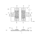
次に、図2(a)及び(b)に示すように、第1のランド12内であって後述する第1の電極51と重なる予定領域上と、第2のランド16内であって後述する第2の電極52(例えば、図3(a)及び(b)参照。)と重なる予定領域上とにそれぞれクリームはんだを塗布して、複数のはんだ部20を形成する。クリームはんだの塗布は、例えばスクリーン印刷で行う。ここで、複数のはんだ部20の各々の平面視による形状(即ち、平面形状)は、互いに同一で同一の大きさ(即ち、合同)であり、例えばY軸方向に長く延びる長方形となっている。第1のランド12上及び第2のランド16上において、長方形のはんだ部20はそれぞれ複数ずつ設けられており、これらはY軸方向と直交するX軸方向において等間隔に配置されている。
Next, as shown in FIGS. 2 (a) and 2 (b), within the
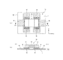
次に、図3(a)及び(b)に示すように、この配線基板10に素子50を実装する。ここで、素子50は、例えばコンデンサであり、第1の電極51と、第2の電極52と、第1の電極51と第2の電極52とに挟まれた誘電体53と、を有する。この素子50の実装工程では、第1のランド12に設けられた複数のはんだ部20と第1の電極51とが重なり、且つ、第2のランド16に設けられた複数のはんだ部20と第2の電極52とが重なるように、ベース基板1の表面1a上に素子50を配置する。そして、この状態で、配線基板10及び素子50をリフロー炉に通す。これにより、複数のはんだ部20がそれぞれ溶融し、第1のランド12上及び第2のランド16上において、それぞれ一つのはんだ層20´を形成する。
Next, as shown in FIGS. 3A and 3B, the
図4(a)及び(b)は、はんだ層20´の形成過程を模式的に示す断面図である。図4(a)に示すように、上記の溶融の過程では、複数のはんだ部20は溶融して、矢印で示すように、複数のはんだ部20の間(即ち、はんだ部20が設けられていない領域)に濡れ広がる。そして、隣り合うはんだ部20同士が接触し、やがて固化して、図4(b)に示すように、第1のランド12上において一つのはんだ層20´となる。図示しないが、第2のランド16上におけるはんだ層20´の形成過程も同様である。これにより、はんだ層20´を介して、第1の電極51と第1のランド12とが接続されると共に、第2の電極52と第2のランド16とが接続されて、電子部品が完成する。
4A and 4B are cross-sectional views schematically showing the formation process of the solder layer 20 '. As shown in FIG. 4A, in the above melting process, the plurality of
以上説明したように、本発明の第1実施形態によれば、素子50を実装する際に、複数のはんだ部20が溶融し、溶融したはんだ(即ち、溶融はんだ)の一部は、はんだ部20が設けられていない領域に濡れ広がって一つのはんだ層20´となる。これにより、第1の電極51と第1のランド12との間に残されるはんだを少なくすることができると共に、第2の電極52と第1のランド16との間に残されるはんだを少なくすることができ、これらの間ではんだ層20´の厚みをそれぞれ小さくすることができる。はんだ層20´を薄く形成することができ、第1の電極51と第1のランド12との間の距離、及び、第2の電極52と第2のランド16との間の距離をそれぞれ縮めることができるので、電子部品の低背化(即ち、部品実装総厚の低背化)を実現することができる。
As described above, according to the first embodiment of the present invention, when the
また、本発明の第1実施形態によれば、複数のはんだ部20の各々の平面形状は例えばY軸方向に長く延びる長方形であり、これらはX軸方向において等間隔に配置されている。これにより、第1、第2のランド12、16上において、溶融はんだの逃げ道(即ち、濡れ広がる経路)が一様に確保されるため、はんだ層20´の厚みの均一化が容易となる。
なお、上記の第1実施形態では、複数のはんだ部20の各々の平面形状が長方形である場合について説明した。しかしながら、本発明において、これらの平面形状は長方形に限定されるものではない。
Further, according to the first embodiment of the present invention, the planar shape of each of the plurality of
In the first embodiment, the case where each planar shape of the plurality of
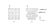
例えば、図5(a)及び(b)に示すように、複数のはんだ部20の各々の平面形状は正方形でもよい。図5(a)に示すように、はんだ部20の平面形状が正方形の場合、これら複数の正方形は互いに離れており、X軸方向及びY軸方向において、それぞれ等間隔に列を成すように配置されていてもよい。又は、図5(b)に示すように、これら複数の正方形は、例えば、X軸方向に並ぶ複数の列が、Y軸方向において等間隔に配置されており、Y軸方向において奇数番目の列と偶数番目の列とが、X軸方向に半ピッチずつ、ずれるように配置されていてもよい。
For example, as shown in FIGS. 5A and 5B, the planar shape of each of the plurality of
或いは、図6(a)及び(b)に示すように、複数のはんだ部20の各々の平面形状は円形(例えば、正円形)でもよい。図6(a)に示すように、これら複数の正円形は互いに離れており、X軸方向及びY軸方向において、それぞれ等間隔に列を成すように配置されていてもよい。又は、図6(b)に示すように、これら複数の正円形は、例えば、X軸方向に並ぶ複数の列が、Y軸方向において等間隔に配置されており、Y軸方向において奇数番目の列と偶数番目の列とが、X軸方向に半ピッチずつ、ずれるように配置されていてもよい。
Or as shown to Fig.6 (a) and (b), each planar shape of the some
或いは、図7(a)及び(b)に示すように、複数のはんだ部20の各々の平面形状は三角形(例えば、正三角形)でもよい。図7(a)に示すように、これら複数の正三角形は互いに離れており、例えば、X軸方向に並ぶ複数の列が、Y軸方向において等間隔に配置されており、Y軸方向において奇数番目の列と偶数番目の列とが、X軸方向に半ピッチずつ、ずれるように配置されていてもよい。又は、図7(a)に示すように、これら複数の正三角形は、X軸方向及びY軸方向においてそれぞれ等間隔に列を成し、且つ、隣り合う正三角形の向かい合う各辺20aが平行となるように、配置されていてもよい。
Alternatively, as shown in FIGS. 7A and 7B, the planar shape of each of the plurality of
或いは、図8に示すように、複数のはんだ部20の各々の平面形状は五角以上の多角形(例えば、正六角形)でもよい。図8に示すように、これら複数の正六角形は互いに離れており、X軸方向及びY軸方向において、それぞれ等間隔に列を成すように配置されていてもよい(即ち、ハニカム構造を成すように配置されていてもよい。)。
このように、複数のはんだ部20の各々の形状及びその配置が、図5(a)〜図8等に示す何れの形態であったとしても、溶融はんだの逃げ道(即ち、濡れ広がる経路)が一様に確保される。このため、長方形の場合と同様の効果を奏することができる。
Alternatively, as shown in FIG. 8, the planar shape of each of the plurality of
Thus, even if the shape and arrangement of each of the plurality of
(2)第2実施形態
上記の第1実施形態では、第1のランドと第2のランドにそれぞれ複数のはんだ部を設ける場合について説明した。しかしながら、本発明では、ランドに複数のはんだ部を設けるのではなく、ランドそのものに複数の開口部を設けるようにしてもよい。
図9(a)〜図11(b)は、本発明の第2実施形態に係る電子部品の製造方法を示す図であり、各図の(a)は平面図、各図の(b)は(a)をX9−X´9線〜X11−X´11線で切断した断面図である。図9(a)に示すように、まず始めに、配線基板60を用意する。この配線基板60は、ベース基板1と、ベース基板1の表面1aに設けられた第1の配線61と、第2の配線65と、を有する。第1の配線61の先端には第1のランド62が設けられており、第2の配線65の先端には第2のランド66が設けられている。
(2) Second Embodiment In the first embodiment described above, the case where a plurality of solder portions are provided on each of the first land and the second land has been described. However, in the present invention, instead of providing a plurality of solder portions on the land, a plurality of openings may be provided on the land itself.
FIG. 9A to FIG. 11B are views showing a method of manufacturing an electronic component according to the second embodiment of the present invention, in which FIG. 9A is a plan view and FIG. It is sectional drawing which cut | disconnected (a) by the X9-X'9 line | wire-X11-X'11 line | wire. As shown in FIG. 9A, first, a
第1のランド62を含む第1の配線61、及び、第2のランド66を含む第2の配線65は、第1実施形態で説明した第1の配線11及び第2の配線15(例えば、図1(a)及び(b)参照。)と同様に、それぞれ銅箔等の金属からなり、その表面はメッキされていてもよい。例えば、第1の配線61及び第2の配線65を構成する金属が銅(Cu)の場合、その表面は金(Au)又はスズ(Sn)でメッキされていてもよい。また、第1のランド62と第2のランド66は平面視で同一の形状(例えば、矩形)で、且つ、同一の大きさである。第1のランド62と第2のランド66は例えばY軸方向において離れた状態で隣り合っている。
The
さらに、図9(a)及び(b)に示すように、第1のランド62内であって第1の電極51と重なる予定領域には、ベース基板1の表面1aを底面とする複数の開口部63が設けられている。第2のランド66の第2の電極52と重なる予定領域にも、ベース基板1の表面1aを底面とする複数の開口部67が設けられている。これら複数の開口部63、67の平面形状は互いに同一で同一の大きさであり、例えばY軸方向に長く延びる長方形となっている。また、これら複数の開口部63、67は、X軸方向において等間隔に設けられている。
Furthermore, as shown in FIGS. 9A and 9B, a plurality of openings having the bottom surface of the
次に、図10(a)及び(b)に示すように、第1のランド62上と第2のランド66上にそれぞれはんだ部70を形成する。ここで、はんだ部70の各々は、例えばクリームはんだであり、その形成はスクリーン印刷で行う。はんだ部70の平面形状は、例えば、上記の開口部63、67をそれぞれ覆う長方形となっている。
次に、図11(a)及び(b)に示すように、この配線基板60に素子50を実装する。この素子50の実装工程では、第1のランド62に設けられたはんだ部70と第1の電極51とが重なり、且つ、第2のランド66に設けられたはんだ部70と第2の電極52とが重なるように、ベース基板1の表面1a上に素子50を配置する。そして、この状態で、配線基板60及び素子50をリフロー炉に通す。これにより、第1のランド62上及び第2のランド66上において、はんだ部70がそれぞれ溶融して、はんだ層70´が形成される。
Next, as shown in FIGS. 10A and 10B,
Next, as shown in FIGS. 11A and 11B, the
図12(a)及び(b)は、はんだ層70´の形成過程を模式的に示す断面図である。図12(a)に示すように、上記の溶融の過程では、第1のランド62上のはんだ部70は溶融し、その一部は矢印で示すように、第1のランド62に設けられた複数の開口部63に入り込む。そして、溶融したはんだは複数の開口部63を埋め込んだ状態で固化して、図12(b)に示すように、はんだ層70´となる。図示しないが、第2のランド66上におけるはんだ層70´の形成過程も同様である。これにより、はんだ層70´を介して、第1の電極51と第1のランド62とが接続されると共に、第2の電極52と第2のランド66とが接続されて、電子部品が完成する。
12A and 12B are cross-sectional views schematically showing the formation process of the solder layer 70 '. As shown in FIG. 12A, in the melting process, the
以上説明したように、本発明の第2実施形態によれば、素子50を実装する際に、第1のランド62に設けられた複数の開口部63内や、第2のランド66に設けられた複数の開口部67内に溶融はんだの一部が入り込む。これにより、第1の電極51と第1のランド62との間に残されるはんだを少なくすることができると共に、第2の電極52と第1のランド66との間に残されるはんだを少なくすることができ、これらの間ではんだ層70´の厚みをそれぞれ小さくすることができる。はんだ層70´を薄く形成することができ、第1の電極51と第1のランド62との間の距離、及び、第2の電極52と第2のランド66との間の距離をそれぞれ縮めることができるので、電子部品の低背化(即ち、部品実装総厚の低背化)を実現することができる。
As described above, according to the second embodiment of the present invention, when the
なお、上記の第1実施形態では、複数の開口部63、67の各々の平面形状がY軸方向に長く延びる長方形である場合について説明した。しかしながら、本発明において、この長方形の向きはY軸方向に限定されるものではない。例えば図13に示すように、複数の開口部63の各々の平面形状はX軸方向に長く延びる長方形であってもよい。また、これら複数の開口部63は、Y軸方向において等間隔に設けられていてもよく、さらに、その一端は第1のランド62の外周の辺に面していてもよい。第2のランド66の複数の開口部67も同様である。このような構成であっても、上記の第1実施形態と同様に、はんだ層70´を薄く形成することができ、電子部品の低背化を実現することができる。
In the first embodiment, the case where each planar shape of the plurality of
また、本発明において、これら複数の開口部63、67の各々の平面形状は、長方形に限定されるものでもない。例えば、図14(a)及び(b)に示すように、複数の開口部63の各々の平面形状は正方形でもよい。また、図15(a)及び(b)に示すように、複数の開口部63の各々の平面形状は正円形でもよい。さらに、図16(a)及び(b)に示すように、複数の開口部63の各々の平面形状は正三角形でもよい。また、図示しないが、複数の開口部63の各々の平面形状は正六角形でもよい。第2のランド66の複数の開口部67も同様である。
このように、複数の開口部63、67の各々の形状及びその配置が、図14(a)〜図16(b)等に示す何れの形態であったとしても、溶融はんだの逃げ道(即ち、濡れ広がる経路)が一様に確保される。このため、長方形の場合と同様の効果を奏することができる。
In the present invention, the planar shape of each of the plurality of
As described above, the shape of each of the plurality of
(3)第3実施形態
また、本発明では、上記の第1実施形態と第2実施形態とを組み合わせてもよい。即ち、ランドの電極と重なり合う予定領域に複数の開口部を設けておき、この複数の開口部の各々と平面視で重なるように複数のはんだ部を設けてもよい。
図17〜図19は、本発明の第3実施形態に係る配線基板80の構成例を示す平面図である。例えば、図17に示すように、第1のランド62に設けられた複数の開口部63の各々と平面視で直交するように、これら複数の開口部63の上に複数のはんだ部20を設けてもよい。同様に、第2のランド66に設けられた複数の開口部67の各々と平面視で直交するように、これら複数の開口部67の上に複数のはんだ部20を設けてもよい。この例では、複数の開口部63、66の各々の平面形状はX軸方向に長く延びる長方形であり、複数のはんだ部20の各々の平面形状はY軸方向に長く延びる長方形である。
(3) Third Embodiment In the present invention, the first embodiment and the second embodiment may be combined. That is, a plurality of openings may be provided in a planned region overlapping with the land electrode, and a plurality of solder portions may be provided so as to overlap each of the plurality of openings in plan view.
FIGS. 17-19 is a top view which shows the structural example of the
このような構成であれば、配線基板80に素子50を実装する際に、複数のはんだ部20が溶融し、溶融はんだの一部は、はんだ部20が設けられていない領域に濡れ広がる。また、溶融はんだの一部は開口部63、67内にそれぞれ入り込む。このため、第1、第2実施形態と比べて、第1の電極51と第1のランド12との間に残されるはんだをより少なくすることができると共に、第2の電極52と第1のランド16との間に残されるはんだをより少なくすることができる。その結果、はんだ層をより薄く形成することが可能となる。
With such a configuration, when the
また、この第3実施形態では、複数の開口部63、67の各々の平面形状を第1の形状とし、複数のはんだ部20の各々の平面形状を第2の形状としたとき、第1の形状と第2の形状は相似であり、且つ、第1の形状よりも第2の形状の方が大きいことが好ましい。また、複数のはんだ部20を設ける工程では、複数の開口部63、67の各々を複数のはんだ部20の各々によって完全に覆うことが好ましい。
In the third embodiment, when the planar shape of each of the plurality of
例えば、図18に示すように、素子が実装される前の配線基板80において、複数の開口部63、67の各々の平面形状(第1の形状)は長方形であり、複数のはんだ部20の各々の平面形状(第2の形状)も長方形である。第1の形状と第2の形状は相似で、且つ、第1の形状よりも第2の形状の方が大きい。しかも、複数のはんだ部20の各々によって、複数の開口部63、67の各々は完全に覆われている。
For example, as shown in FIG. 18, in the
或いは、図19に示すように、素子が実装される前の配線基板80において、複数の開口部63、67の各々の平面形状(第1の形状)は正円形であり、複数のはんだ部20の各々の平面形状(第2の形状)も正円形である。第1の形状と第2の形状とが相似で、且つ、第1の形状よりも第2の形状の方が大きい。しかも、複数のはんだ部20の各々によって、複数の開口部63、67の各々は完全に覆われている。
Alternatively, as shown in FIG. 19, in the
素子の実装工程では、このような配線基板80を用いることにより、複数の開口部63、67内へ溶融はんだを容易に入り込ませることができる。また、複数の開口部63、67の各々の平面形状よりも、複数のはんだ部20の各々の平面形状の方が大きいため、第1の電極51と第1のランド62との間の接続、及び、第2の電極52と第2のランド66との間の接続、にそれぞれ必要なはんだを容易に残すことができる。
In the element mounting process, by using such a
なお、この第3実施形態では、第1の形状と第2の形状がそれぞれ長方形、又は、正円形である場合を示したが、本発明において、第1の形状と第2の形状はこれらに限定されるものではない。例えば、第1、第2実施形態と同様、第1の形状と第2の形状は正三角形や五六角形であってもよい。このような場合であっても、図17〜図19に示した各例と同様の効果を奏することができる。 In the third embodiment, the first shape and the second shape are each a rectangle or a regular circle. However, in the present invention, the first shape and the second shape are the same. It is not limited. For example, as in the first and second embodiments, the first shape and the second shape may be regular triangles or pentagons. Even in such a case, the same effects as in the examples shown in FIGS. 17 to 19 can be obtained.
(4)その他の実施形態
なお、本発明において、ベース基板1はフレキシブル基板に限定されるものではなく、リジッド基板であってもよい。また、ベース基板1の材料は、ポリイミドに限定されるものではなく、フェノール、エポキシ、ガラスエポキシ、テフロン(登録商標)、アルミナ、PET(ポリエチレンテレフタラート)、PEN(ポリエチレンナフタレート)などの各絶縁材を用いることができる。
(4) Other Embodiments In the present invention, the
また、本発明において、第1の配線11、61、第2の配線15、65の各材料も、銅(Cu)に限定されるものではなく、アルミニウム、黒鉛などの各導電材を用いることができる。
また、本発明において、素子50はコンデンサに限定されるものではない。素子50は、例えば抵抗素子などでもよく、その場合は第1の電極51と第2の電極52との間に抵抗体が配置される。
In the present invention, the materials of the
In the present invention, the
1 ベース基板、1a 表面、10、60、80 配線基板、11、61 第1の配線、12、62 第1のランド、15、65 第2の配線、16、66 第2のランド、20、70 (溶融前の)はんだ部、20´、70´ (溶融後の)はんだ層、50 素子(例えば、コンデンサ、又は、抵抗素子)、51 第1の電極、52 第2の電極、53 誘電体
DESCRIPTION OF
Claims (8)
前記複数のはんだ部と素子の電極とが接するように前記素子を配置する工程と、
前記複数のはんだ部を加熱し溶融させてはんだ層を形成し、前記はんだ層を介して前記電極と前記ランドとを接続する工程と、を含むことを特徴とする電子部品の製造方法。 Providing a plurality of solder portions on a land provided on the substrate;
Arranging the element so that the plurality of solder portions and the electrode of the element are in contact with each other;
The method of manufacturing an electronic component comprising: a step of heating and melting the plurality of solder portions to form a solder layer, and connecting the electrode and the land via the solder layer.
前記電極と前記ランドとを接続する工程では、前記複数のはんだ部の溶融した一部を前記開口部内に入り込ませることを特徴とする請求項1に記載の電子部品の製造方法。 An opening is provided in a region of the land that overlaps the electrode;
2. The method of manufacturing an electronic component according to claim 1, wherein in the step of connecting the electrode and the land, molten portions of the plurality of solder portions are caused to enter the opening.
前記複数の開口部の各々の平面視による形状を第1の形状とし、前記複数のはんだ部の各々の平面視による形状を第2の形状としたとき、前記第1の形状と前記第2の形状は相似であり、且つ、前記第1の形状よりも前記第2の形状の方が大きく、
前記複数のはんだ部を設ける工程では、前記複数の開口部の各々を前記複数のはんだ部の各々で覆うことを特徴とする請求項2に記載の電子部品の製造方法。 The land is provided with a plurality of openings as the openings,
When the shape of each of the plurality of openings in plan view is the first shape, and the shape of each of the plurality of solder portions in plan view is the second shape, the first shape and the second shape The shape is similar and the second shape is larger than the first shape,
The method of manufacturing an electronic component according to claim 2, wherein, in the step of providing the plurality of solder portions, each of the plurality of openings is covered with each of the plurality of solder portions.
前記複数のはんだ部の各々を平面視で同一の形状で同一の大きさに形成し、等間隔に配置することを特徴とする請求項1から請求項3の何れか一項に記載の電子部品の製造方法。 In the step of providing the plurality of solder portions,
4. The electronic component according to claim 1, wherein each of the plurality of solder portions has the same shape and the same size in a plan view, and is arranged at equal intervals. 5. Manufacturing method.
前記はんだ部と素子の電極とが接するように前記素子を配置する工程と、
前記はんだ部を加熱し溶融させてはんだ層を形成し、前記はんだ層を介して前記電極と前記ランドとを接続する工程と、を含み、
前記ランドには開口部が設けられており、
前記電極と前記ランドとを接続する工程では、前記はんだ部の溶融した一部を前記開口部内に入り込ませることを特徴とする電子部品の製造方法。 Providing a solder portion on a land provided on the substrate;
Arranging the element so that the solder portion and the electrode of the element are in contact with each other;
Heating and melting the solder portion to form a solder layer, and connecting the electrode and the land via the solder layer,
The land is provided with an opening,
In the step of connecting the electrode and the land, a molten part of the solder part is caused to enter the opening part.
基板と、
前記基板に設けられたランドと、
前記ランドの前記電極と重なり合う予定領域に設けられた複数のはんだ部と、を備えることを特徴とする配線基板。 A wiring board to which elements having electrodes are attached,
A substrate,
Lands provided on the substrate;
A wiring board comprising: a plurality of solder portions provided in a predetermined region overlapping the electrode of the land.
前記開口部のうちの少なくとも一部と前記複数のはんだ部とが平面視で重なっていることを特徴とする請求項6に記載の配線基板。 An opening is provided in a region of the land that overlaps the electrode;
The wiring board according to claim 6, wherein at least a part of the opening portion and the plurality of solder portions overlap in a plan view.
基板と、
前記基板に設けられたランドと、を備え、
前記ランドの前記電極と重なり合う予定領域に開口部が設けられていることを特徴とする配線基板。
A wiring board to which elements having electrodes are attached,
A substrate,
A land provided on the substrate,
A wiring board, wherein an opening is provided in a region of the land that overlaps the electrode.
Priority Applications (1)
| Application Number | Priority Date | Filing Date | Title |
|---|---|---|---|
| JP2011073573A JP5640861B2 (en) | 2011-03-29 | 2011-03-29 | Electronic component manufacturing method and wiring board |
Applications Claiming Priority (1)
| Application Number | Priority Date | Filing Date | Title |
|---|---|---|---|
| JP2011073573A JP5640861B2 (en) | 2011-03-29 | 2011-03-29 | Electronic component manufacturing method and wiring board |
Publications (2)
| Publication Number | Publication Date |
|---|---|
| JP2012209408A true JP2012209408A (en) | 2012-10-25 |
| JP5640861B2 JP5640861B2 (en) | 2014-12-17 |
Family
ID=47188913
Family Applications (1)
| Application Number | Title | Priority Date | Filing Date |
|---|---|---|---|
| JP2011073573A Active JP5640861B2 (en) | 2011-03-29 | 2011-03-29 | Electronic component manufacturing method and wiring board |
Country Status (1)
| Country | Link |
|---|---|
| JP (1) | JP5640861B2 (en) |
Cited By (1)
| Publication number | Priority date | Publication date | Assignee | Title |
|---|---|---|---|---|
| JP2016039181A (en) * | 2014-08-05 | 2016-03-22 | キヤノン株式会社 | Method of manufacturing module |
Citations (8)
| Publication number | Priority date | Publication date | Assignee | Title |
|---|---|---|---|---|
| JPH03284895A (en) * | 1990-03-30 | 1991-12-16 | Taiyo Yuden Co Ltd | Printing of pastelike solder |
| JPH044779U (en) * | 1990-04-26 | 1992-01-16 | ||
| JPH0878824A (en) * | 1994-08-29 | 1996-03-22 | Whitaker Corp:The | Connected plate |
| JP2005210022A (en) * | 2004-01-26 | 2005-08-04 | Fujikura Ltd | Printed wiring board and its production method |
| JP2005294632A (en) * | 2004-04-01 | 2005-10-20 | Hitachi Ltd | Surface mount device soldering structure |
| JP2006287060A (en) * | 2005-04-01 | 2006-10-19 | Sony Corp | Circuit board and chip component soldering structure |
| JP2009224697A (en) * | 2008-03-18 | 2009-10-01 | Asmo Co Ltd | Printed circuit board and electronic component mounting substrate |
| JP2010283039A (en) * | 2009-06-02 | 2010-12-16 | Nec Access Technica Ltd | Method of soldering electronic component and substrate for mounting electronic component |
-
2011
- 2011-03-29 JP JP2011073573A patent/JP5640861B2/en active Active
Patent Citations (8)
| Publication number | Priority date | Publication date | Assignee | Title |
|---|---|---|---|---|
| JPH03284895A (en) * | 1990-03-30 | 1991-12-16 | Taiyo Yuden Co Ltd | Printing of pastelike solder |
| JPH044779U (en) * | 1990-04-26 | 1992-01-16 | ||
| JPH0878824A (en) * | 1994-08-29 | 1996-03-22 | Whitaker Corp:The | Connected plate |
| JP2005210022A (en) * | 2004-01-26 | 2005-08-04 | Fujikura Ltd | Printed wiring board and its production method |
| JP2005294632A (en) * | 2004-04-01 | 2005-10-20 | Hitachi Ltd | Surface mount device soldering structure |
| JP2006287060A (en) * | 2005-04-01 | 2006-10-19 | Sony Corp | Circuit board and chip component soldering structure |
| JP2009224697A (en) * | 2008-03-18 | 2009-10-01 | Asmo Co Ltd | Printed circuit board and electronic component mounting substrate |
| JP2010283039A (en) * | 2009-06-02 | 2010-12-16 | Nec Access Technica Ltd | Method of soldering electronic component and substrate for mounting electronic component |
Cited By (2)
| Publication number | Priority date | Publication date | Assignee | Title |
|---|---|---|---|---|
| JP2016039181A (en) * | 2014-08-05 | 2016-03-22 | キヤノン株式会社 | Method of manufacturing module |
| US9815133B2 (en) | 2014-08-05 | 2017-11-14 | Canon Kabushiki Kaisha | Method for producing a module |
Also Published As
| Publication number | Publication date |
|---|---|
| JP5640861B2 (en) | 2014-12-17 |
Similar Documents
| Publication | Publication Date | Title |
|---|---|---|
| JP2009135470A (en) | Mounting structure | |
| JP2008226945A (en) | Semiconductor device and manufacturing method thereof | |
| JP2010135671A (en) | Semiconductor equipment and method of manufacturing the same | |
| JP2013074054A (en) | Electronic device, wiring board, and electronic device manufacturing method | |
| JP2015115419A (en) | Semiconductor package and manufacturing method thereof | |
| US20150062849A1 (en) | Printed wiring board | |
| JP5640861B2 (en) | Electronic component manufacturing method and wiring board | |
| JP2012164934A (en) | Circuit module, electronic component mounting board and circuit module manufacturing method | |
| JPWO2009110355A1 (en) | Mounting structure and manufacturing method thereof | |
| JP2010232616A (en) | Semiconductor device and wiring board | |
| JPWO2018037871A1 (en) | Resin multilayer substrate, transmission line, module, and module manufacturing method | |
| JP5587804B2 (en) | Manufacturing method of wiring board for mounting electronic component, wiring board for mounting electronic component, and manufacturing method of wiring board with electronic component | |
| KR20130086110A (en) | Assembly of multi-pattern wiring substrate and method of assembling multi-pattern wiring substrate | |
| JP2024134789A (en) | Semiconductor device and wiring board | |
| JP2015146404A (en) | Semiconductor device and manufacturing method of the same | |
| KR20150026053A (en) | Semiconductor packages having passive components and methods for fabricating the same | |
| JP2005251856A (en) | Semiconductor device | |
| JP2012209383A (en) | Multilayer substrate and method of manufacturing the same | |
| JP2011009488A (en) | Semiconductor device, and method of manufacturing the same | |
| JP4068575B2 (en) | Wiring substrate manufacturing method and semiconductor device manufacturing method | |
| JP7826616B2 (en) | Joint for electronic device and method for joining electronic components | |
| JP2012199269A (en) | Electronic component, method of manufacturing the same, and wiring substrate | |
| JP2006041238A (en) | Wiring board and method of manufacturing wiring board | |
| TW201113964A (en) | Method for manufacturing semiconductor device | |
| JP2013073990A (en) | Multilayer printed circuit board and method for manufacturing the same |
Legal Events
| Date | Code | Title | Description |
|---|---|---|---|
| A621 | Written request for application examination |
Free format text: JAPANESE INTERMEDIATE CODE: A621 Effective date: 20131213 |
|
| A977 | Report on retrieval |
Free format text: JAPANESE INTERMEDIATE CODE: A971007 Effective date: 20140626 |
|
| A131 | Notification of reasons for refusal |
Free format text: JAPANESE INTERMEDIATE CODE: A131 Effective date: 20140722 |
|
| A521 | Written amendment |
Free format text: JAPANESE INTERMEDIATE CODE: A523 Effective date: 20140910 |
|
| TRDD | Decision of grant or rejection written | ||
| A01 | Written decision to grant a patent or to grant a registration (utility model) |
Free format text: JAPANESE INTERMEDIATE CODE: A01 Effective date: 20140930 |
|
| A61 | First payment of annual fees (during grant procedure) |
Free format text: JAPANESE INTERMEDIATE CODE: A61 Effective date: 20141013 |
|
| R150 | Certificate of patent or registration of utility model |
Ref document number: 5640861 Country of ref document: JP Free format text: JAPANESE INTERMEDIATE CODE: R150 |
|
| S531 | Written request for registration of change of domicile |
Free format text: JAPANESE INTERMEDIATE CODE: R313531 |
|
| R350 | Written notification of registration of transfer |
Free format text: JAPANESE INTERMEDIATE CODE: R350 |