JP2012247770A - 表示装置 - Google Patents
表示装置 Download PDFInfo
- Publication number
- JP2012247770A JP2012247770A JP2012007717A JP2012007717A JP2012247770A JP 2012247770 A JP2012247770 A JP 2012247770A JP 2012007717 A JP2012007717 A JP 2012007717A JP 2012007717 A JP2012007717 A JP 2012007717A JP 2012247770 A JP2012247770 A JP 2012247770A
- Authority
- JP
- Japan
- Prior art keywords
- display panel
- hole
- circuit board
- display device
- printed circuit
- Prior art date
- Legal status (The legal status is an assumption and is not a legal conclusion. Google has not performed a legal analysis and makes no representation as to the accuracy of the status listed.)
- Granted
Links
Images


Classifications
-
- G—PHYSICS
- G02—OPTICS
- G02F—OPTICAL DEVICES OR ARRANGEMENTS FOR THE CONTROL OF LIGHT BY MODIFICATION OF THE OPTICAL PROPERTIES OF THE MEDIA OF THE ELEMENTS INVOLVED THEREIN; NON-LINEAR OPTICS; FREQUENCY-CHANGING OF LIGHT; OPTICAL LOGIC ELEMENTS; OPTICAL ANALOGUE/DIGITAL CONVERTERS
- G02F1/00—Devices or arrangements for the control of the intensity, colour, phase, polarisation or direction of light arriving from an independent light source, e.g. switching, gating or modulating; Non-linear optics
- G02F1/01—Devices or arrangements for the control of the intensity, colour, phase, polarisation or direction of light arriving from an independent light source, e.g. switching, gating or modulating; Non-linear optics for the control of the intensity, phase, polarisation or colour
- G02F1/13—Devices or arrangements for the control of the intensity, colour, phase, polarisation or direction of light arriving from an independent light source, e.g. switching, gating or modulating; Non-linear optics for the control of the intensity, phase, polarisation or colour based on liquid crystals, e.g. single liquid crystal display cells
- G02F1/133—Constructional arrangements; Operation of liquid crystal cells; Circuit arrangements
- G02F1/1333—Constructional arrangements; Manufacturing methods
-
- G—PHYSICS
- G02—OPTICS
- G02F—OPTICAL DEVICES OR ARRANGEMENTS FOR THE CONTROL OF LIGHT BY MODIFICATION OF THE OPTICAL PROPERTIES OF THE MEDIA OF THE ELEMENTS INVOLVED THEREIN; NON-LINEAR OPTICS; FREQUENCY-CHANGING OF LIGHT; OPTICAL LOGIC ELEMENTS; OPTICAL ANALOGUE/DIGITAL CONVERTERS
- G02F1/00—Devices or arrangements for the control of the intensity, colour, phase, polarisation or direction of light arriving from an independent light source, e.g. switching, gating or modulating; Non-linear optics
- G02F1/01—Devices or arrangements for the control of the intensity, colour, phase, polarisation or direction of light arriving from an independent light source, e.g. switching, gating or modulating; Non-linear optics for the control of the intensity, phase, polarisation or colour
- G02F1/13—Devices or arrangements for the control of the intensity, colour, phase, polarisation or direction of light arriving from an independent light source, e.g. switching, gating or modulating; Non-linear optics for the control of the intensity, phase, polarisation or colour based on liquid crystals, e.g. single liquid crystal display cells
- G02F1/133—Constructional arrangements; Operation of liquid crystal cells; Circuit arrangements
- G02F1/1333—Constructional arrangements; Manufacturing methods
- G02F1/1345—Conductors connecting electrodes to cell terminals
- G02F1/13452—Conductors connecting driver circuitry and terminals of panels
-
- G—PHYSICS
- G02—OPTICS
- G02F—OPTICAL DEVICES OR ARRANGEMENTS FOR THE CONTROL OF LIGHT BY MODIFICATION OF THE OPTICAL PROPERTIES OF THE MEDIA OF THE ELEMENTS INVOLVED THEREIN; NON-LINEAR OPTICS; FREQUENCY-CHANGING OF LIGHT; OPTICAL LOGIC ELEMENTS; OPTICAL ANALOGUE/DIGITAL CONVERTERS
- G02F1/00—Devices or arrangements for the control of the intensity, colour, phase, polarisation or direction of light arriving from an independent light source, e.g. switching, gating or modulating; Non-linear optics
- G02F1/01—Devices or arrangements for the control of the intensity, colour, phase, polarisation or direction of light arriving from an independent light source, e.g. switching, gating or modulating; Non-linear optics for the control of the intensity, phase, polarisation or colour
- G02F1/13—Devices or arrangements for the control of the intensity, colour, phase, polarisation or direction of light arriving from an independent light source, e.g. switching, gating or modulating; Non-linear optics for the control of the intensity, phase, polarisation or colour based on liquid crystals, e.g. single liquid crystal display cells
- G02F1/133—Constructional arrangements; Operation of liquid crystal cells; Circuit arrangements
- G02F1/1333—Constructional arrangements; Manufacturing methods
- G02F1/133308—Support structures for LCD panels, e.g. frames or bezels
-
- G—PHYSICS
- G02—OPTICS
- G02F—OPTICAL DEVICES OR ARRANGEMENTS FOR THE CONTROL OF LIGHT BY MODIFICATION OF THE OPTICAL PROPERTIES OF THE MEDIA OF THE ELEMENTS INVOLVED THEREIN; NON-LINEAR OPTICS; FREQUENCY-CHANGING OF LIGHT; OPTICAL LOGIC ELEMENTS; OPTICAL ANALOGUE/DIGITAL CONVERTERS
- G02F1/00—Devices or arrangements for the control of the intensity, colour, phase, polarisation or direction of light arriving from an independent light source, e.g. switching, gating or modulating; Non-linear optics
- G02F1/01—Devices or arrangements for the control of the intensity, colour, phase, polarisation or direction of light arriving from an independent light source, e.g. switching, gating or modulating; Non-linear optics for the control of the intensity, phase, polarisation or colour
- G02F1/13—Devices or arrangements for the control of the intensity, colour, phase, polarisation or direction of light arriving from an independent light source, e.g. switching, gating or modulating; Non-linear optics for the control of the intensity, phase, polarisation or colour based on liquid crystals, e.g. single liquid crystal display cells
- G02F1/133—Constructional arrangements; Operation of liquid crystal cells; Circuit arrangements
- G02F1/1333—Constructional arrangements; Manufacturing methods
- G02F1/1335—Structural association of cells with optical devices, e.g. polarisers or reflectors
-
- G—PHYSICS
- G02—OPTICS
- G02F—OPTICAL DEVICES OR ARRANGEMENTS FOR THE CONTROL OF LIGHT BY MODIFICATION OF THE OPTICAL PROPERTIES OF THE MEDIA OF THE ELEMENTS INVOLVED THEREIN; NON-LINEAR OPTICS; FREQUENCY-CHANGING OF LIGHT; OPTICAL LOGIC ELEMENTS; OPTICAL ANALOGUE/DIGITAL CONVERTERS
- G02F2201/00—Constructional arrangements not provided for in groups G02F1/00 - G02F7/00
- G02F2201/46—Fixing elements
Landscapes
- Physics & Mathematics (AREA)
- Nonlinear Science (AREA)
- Mathematical Physics (AREA)
- Chemical & Material Sciences (AREA)
- Crystallography & Structural Chemistry (AREA)
- General Physics & Mathematics (AREA)
- Optics & Photonics (AREA)
- Devices For Indicating Variable Information By Combining Individual Elements (AREA)
- Liquid Crystal (AREA)
Abstract
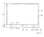
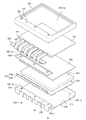
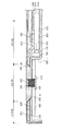
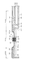
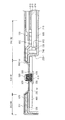
【解決手段】本発明の一実施形態による表示装置は、光を受信して映像を表示する表示パネルと、前記表示パネルを収納する下部シャーシと、前記表示パネルを介して前記下部シャーシと対向し、前記表示パネルの少なくとも一部をカバーし、一側部の厚さ方向に延長した少なくとも1つの第1スルーホールを有する上部シャーシと、電気信号を供給し、前記上部シャーシの一側部の下側に配置され、前記一側部をカバーして前記第1スルーホールに対応する第2スルーホールを有する印刷回路基板と、前記第1スルーホール及び前記第2スルーホールに挿入されて前記上部シャーシと前記印刷回路基板とを結合する結合部材と、を含むことを特徴とする。
【選択図】図2
Description
200…下部シャーシ
300…上部シャーシ
400…印刷回路基板
500…結合部材
600…モールドフレーム
700…光源
800…導光板
820…反射シート
840…光学シート
FP1…フレキシブル回路基板
Claims (10)
- 光を受信して映像を表示する表示パネルと、
前記表示パネルを収納する下部シャーシと、
前記表示パネルを介して前記下部シャーシと対向し、前記表示パネルの少なくとも一部をカバーし、一側部の厚さ方向に延長した少なくとも1つの第1スルーホールを有する上部シャーシと、
前記表示パネルに電気信号を供給し、前記上部シャーシの一側部の下側に配置され、前記一側部をカバーして前記第1スルーホールに対応する第2スルーホールを有する印刷回路基板と、
前記第1スルーホール及び前記第2スルーホールに挿入されて前記上部シャーシと前記印刷回路基板とを結合する結合部材と、
を含むことを特徴とする表示装置。 - 前記第1スルーホールは、内壁に第1ネジ山及び第1ネジ谷を含むことを特徴とする請求項1に記載の表示装置。
- 前記結合部材は、前記第1ネジ山及び前記第1ネジ谷と結合される第2ネジ谷及び第2ネジ山を含むことを特徴とする請求項2に記載の表示装置。
- 前記上部シャーシの一側部は平面の上で前記第1スルーホールを内部に有する第1領域と前記第1領域に隣接する第2領域とを含むことを特徴とする請求項3に記載の表示装置。
- 前記上部シャーシの前記第1領域は前記第2領域よりも膜厚が厚いことを特徴とする請求項4に記載の表示装置。
- 前記下部シャーシは、
底部、
前記底部から前記上部シャーシに向かって延長された側壁部、
前記側壁部から折曲されて延長され、前記上部シャーシの前記一側部と前記印刷回路基板との間に配置された結合部を含むことを特徴とする請求項4に記載の表示装置。 - 前記第1スルーホールは複数個提供され、前記複数の第1スルーホールは前記印刷回路基板が延長された方向に連続して一定な間隔で配置されたことを特徴とする請求項1に記載の表示装置。
- 前記下部シャーシに収納され、前記光を生成する光源と、
前記表示パネルの下側に配置され、前記光源で出射された光をガイドして前記表示パネルに提供する導光板をさらに含むことを特徴とする請求項1に記載の表示装置。 - 前記導光板は複数の側面を具備し、
前記光源は前記導光板の側面の中で少なくとも1つの側面に対向して配置されたことを特徴とする請求項8に記載の表示装置。 - 光を受信して映像を表示する表示パネルと、
前記表示パネルと並べて配置され、前記表示パネルに電気信号を供給し、少なくとも1つの第1スルーホールを具備する印刷回路基板と、
前記表示パネルの少なくとも一部をカバーする第1カバー領域及び前記印刷回路基板をカバーする第2カバー領域を含み、前記第2領域に前記第1スルーホールに対応する第2スルーホールを含む上部シャーシと、
前記表示パネルを収納し前記表示パネルを介して前記上部シャーシと対向する下部シャーシと、
前記第1スルーホール及び前記第2スルーホールに挿入されて前記印刷回路基板と前記上部シャーシを結合する結合部材と、
を含むことを特徴とする表示装置。
Applications Claiming Priority (2)
| Application Number | Priority Date | Filing Date | Title |
|---|---|---|---|
| KR1020110050313A KR101813700B1 (ko) | 2011-05-26 | 2011-05-26 | 표시장치 |
| KR10-2011-0050313 | 2011-05-26 |
Publications (2)
| Publication Number | Publication Date |
|---|---|
| JP2012247770A true JP2012247770A (ja) | 2012-12-13 |
| JP6073060B2 JP6073060B2 (ja) | 2017-02-01 |
Family
ID=47198141
Family Applications (1)
| Application Number | Title | Priority Date | Filing Date |
|---|---|---|---|
| JP2012007717A Active JP6073060B2 (ja) | 2011-05-26 | 2012-01-18 | 表示装置 |
Country Status (4)
| Country | Link |
|---|---|
| US (1) | US8702296B2 (ja) |
| JP (1) | JP6073060B2 (ja) |
| KR (1) | KR101813700B1 (ja) |
| CN (1) | CN102798996B (ja) |
Cited By (2)
| Publication number | Priority date | Publication date | Assignee | Title |
|---|---|---|---|---|
| JP2025106232A (ja) * | 2021-03-23 | 2025-07-15 | アップル インコーポレイテッド | 成形ポリマー構造体を有する電子デバイス |
| JP7860287B2 (ja) | 2021-03-23 | 2026-05-15 | アップル インコーポレイテッド | 成形ポリマー構造体を有する電子デバイス |
Families Citing this family (11)
| Publication number | Priority date | Publication date | Assignee | Title |
|---|---|---|---|---|
| KR20130045569A (ko) * | 2011-10-26 | 2013-05-06 | 삼성디스플레이 주식회사 | 액정 표시 장치 |
| KR20160100006A (ko) * | 2015-02-13 | 2016-08-23 | 삼성디스플레이 주식회사 | 디스플레이 장치용 구조체 및 이를 포함하는 디스플레이 장치 |
| CN107193333B (zh) * | 2017-06-19 | 2020-06-23 | 京东方科技集团股份有限公司 | 显示装置及其显示模块 |
| KR102493330B1 (ko) * | 2018-03-22 | 2023-01-31 | 삼성디스플레이 주식회사 | 수납 부재 및 이를 포함하는 표시 모듈 어셈블리 |
| CN109300404B (zh) * | 2018-11-30 | 2021-07-02 | 云谷(固安)科技有限公司 | 一种显示面板及显示装置 |
| CN110045545B (zh) * | 2019-05-17 | 2022-04-29 | 上海中航光电子有限公司 | 显示装置 |
| CN110910773B (zh) * | 2019-07-26 | 2022-05-24 | 友达光电股份有限公司 | 显示装置 |
| CN116529689A (zh) * | 2020-11-27 | 2023-08-01 | 三星电子株式会社 | 包括显示器的电子装置 |
| WO2022114565A1 (ko) * | 2020-11-27 | 2022-06-02 | 삼성전자 주식회사 | 디스플레이를 포함하는 전자 장치 |
| EP4206805B1 (en) | 2020-11-27 | 2026-03-18 | Samsung Electronics Co., Ltd. | Electronic device comprising display |
| CN113835269B (zh) * | 2021-10-08 | 2023-08-29 | 厦门天马微电子有限公司 | 一种背光模组及显示装置 |
Citations (4)
| Publication number | Priority date | Publication date | Assignee | Title |
|---|---|---|---|---|
| JPH0996799A (ja) * | 1995-10-02 | 1997-04-08 | Hitachi Ltd | 液晶表示装置 |
| JPH1069236A (ja) * | 1996-08-27 | 1998-03-10 | Toshiba Corp | 平面表示装置 |
| JPH10311974A (ja) * | 1998-05-06 | 1998-11-24 | Citizen Watch Co Ltd | 液晶表示装置 |
| JPH11281963A (ja) * | 1998-03-27 | 1999-10-15 | Toshiba Corp | 平面表示装置 |
Family Cites Families (5)
| Publication number | Priority date | Publication date | Assignee | Title |
|---|---|---|---|---|
| JP2005017890A (ja) | 2003-06-27 | 2005-01-20 | Sanyo Electric Co Ltd | 液晶表示装置 |
| KR20060121433A (ko) * | 2005-05-24 | 2006-11-29 | 삼성전자주식회사 | 평판 표시장치 |
| JP4538743B2 (ja) * | 2005-08-30 | 2010-09-08 | ソニー株式会社 | ディスプレイ装置及び情報処理装置 |
| KR101419374B1 (ko) * | 2007-11-07 | 2014-07-14 | 삼성디스플레이 주식회사 | 액정 표시 장치 |
| KR101293551B1 (ko) * | 2008-02-20 | 2013-08-06 | 엘지디스플레이 주식회사 | 액정표시장치 모듈 |
-
2011
- 2011-05-26 KR KR1020110050313A patent/KR101813700B1/ko active Active
- 2011-10-27 US US13/282,621 patent/US8702296B2/en active Active
-
2012
- 2012-01-04 CN CN201210004576.6A patent/CN102798996B/zh active Active
- 2012-01-18 JP JP2012007717A patent/JP6073060B2/ja active Active
Patent Citations (4)
| Publication number | Priority date | Publication date | Assignee | Title |
|---|---|---|---|---|
| JPH0996799A (ja) * | 1995-10-02 | 1997-04-08 | Hitachi Ltd | 液晶表示装置 |
| JPH1069236A (ja) * | 1996-08-27 | 1998-03-10 | Toshiba Corp | 平面表示装置 |
| JPH11281963A (ja) * | 1998-03-27 | 1999-10-15 | Toshiba Corp | 平面表示装置 |
| JPH10311974A (ja) * | 1998-05-06 | 1998-11-24 | Citizen Watch Co Ltd | 液晶表示装置 |
Cited By (3)
| Publication number | Priority date | Publication date | Assignee | Title |
|---|---|---|---|---|
| JP2025106232A (ja) * | 2021-03-23 | 2025-07-15 | アップル インコーポレイテッド | 成形ポリマー構造体を有する電子デバイス |
| US12628293B2 (en) | 2021-03-23 | 2026-05-12 | Apple Inc. | Electronic devices with molded polymer structures |
| JP7860287B2 (ja) | 2021-03-23 | 2026-05-15 | アップル インコーポレイテッド | 成形ポリマー構造体を有する電子デバイス |
Also Published As
| Publication number | Publication date |
|---|---|
| US20120300490A1 (en) | 2012-11-29 |
| US8702296B2 (en) | 2014-04-22 |
| KR20120131855A (ko) | 2012-12-05 |
| CN102798996A (zh) | 2012-11-28 |
| JP6073060B2 (ja) | 2017-02-01 |
| CN102798996B (zh) | 2017-01-18 |
| KR101813700B1 (ko) | 2018-01-02 |
Similar Documents
| Publication | Publication Date | Title |
|---|---|---|
| JP6073060B2 (ja) | 表示装置 | |
| US9488772B2 (en) | Display device, electronic apparatus and illumination device | |
| JP5495364B2 (ja) | 液晶表示装置 | |
| CN102563451B (zh) | 背光组件和装配显示设备的方法 | |
| KR20110059305A (ko) | 액정표시장치 | |
| US8210718B2 (en) | Light source module | |
| JP4743104B2 (ja) | バックライト装置及び液晶表示装置 | |
| JP2010182510A (ja) | バックライトユニット及びこれを用いた液晶表示装置 | |
| KR20170012659A (ko) | 백라이트 유닛 및 이를 포함하는 액정 표시 장치 | |
| CN102445775A (zh) | 光提供组件和显示设备 | |
| JP2008166304A (ja) | バックライト装置及び液晶表示装置 | |
| KR20160022420A (ko) | 표시장치 | |
| KR101792103B1 (ko) | 액정표시장치 | |
| JP2012134496A (ja) | Led光源モジュール及びこれを備えるディスプレイ装置 | |
| WO2013039001A1 (ja) | 照明装置、表示装置、及びテレビ受信装置 | |
| JP2008152101A (ja) | バックライト装置及び液晶表示装置 | |
| JP2010015853A (ja) | 照明装置、液晶表示装置および電子機器 | |
| JP2009205866A (ja) | 照明ユニット及び液晶表示装置 | |
| JP2014095792A (ja) | 液晶表示装置 | |
| JP2007005309A5 (ja) | ||
| JP2013048076A (ja) | 照明装置、表示装置および電子機器 | |
| JP2014096347A (ja) | バックライトユニット及びこれを含む表示装置 | |
| US20130308296A1 (en) | Top chassis assembly and display device having the same | |
| JP5576503B2 (ja) | 光源装置及び表示装置 | |
| JP2008140646A (ja) | バックライト装置及び液晶表示装置 |
Legal Events
| Date | Code | Title | Description |
|---|---|---|---|
| A711 | Notification of change in applicant |
Free format text: JAPANESE INTERMEDIATE CODE: A712 Effective date: 20121213 |
|
| A621 | Written request for application examination |
Free format text: JAPANESE INTERMEDIATE CODE: A621 Effective date: 20141126 |
|
| A977 | Report on retrieval |
Free format text: JAPANESE INTERMEDIATE CODE: A971007 Effective date: 20150826 |
|
| A131 | Notification of reasons for refusal |
Free format text: JAPANESE INTERMEDIATE CODE: A131 Effective date: 20150908 |
|
| A601 | Written request for extension of time |
Free format text: JAPANESE INTERMEDIATE CODE: A601 Effective date: 20151208 |
|
| A521 | Request for written amendment filed |
Free format text: JAPANESE INTERMEDIATE CODE: A523 Effective date: 20160107 |
|
| A131 | Notification of reasons for refusal |
Free format text: JAPANESE INTERMEDIATE CODE: A131 Effective date: 20160419 |
|
| A601 | Written request for extension of time |
Free format text: JAPANESE INTERMEDIATE CODE: A601 Effective date: 20160715 |
|
| A521 | Request for written amendment filed |
Free format text: JAPANESE INTERMEDIATE CODE: A523 Effective date: 20160913 |
|
| TRDD | Decision of grant or rejection written | ||
| A01 | Written decision to grant a patent or to grant a registration (utility model) |
Free format text: JAPANESE INTERMEDIATE CODE: A01 Effective date: 20161206 |
|
| A61 | First payment of annual fees (during grant procedure) |
Free format text: JAPANESE INTERMEDIATE CODE: A61 Effective date: 20170104 |
|
| R150 | Certificate of patent or registration of utility model |
Ref document number: 6073060 Country of ref document: JP Free format text: JAPANESE INTERMEDIATE CODE: R150 |
|
| R250 | Receipt of annual fees |
Free format text: JAPANESE INTERMEDIATE CODE: R250 |
|
| R250 | Receipt of annual fees |
Free format text: JAPANESE INTERMEDIATE CODE: R250 |
|
| R250 | Receipt of annual fees |
Free format text: JAPANESE INTERMEDIATE CODE: R250 |
|
| RD02 | Notification of acceptance of power of attorney |
Free format text: JAPANESE INTERMEDIATE CODE: R3D02 |
|
| R250 | Receipt of annual fees |
Free format text: JAPANESE INTERMEDIATE CODE: R250 |
|
| R250 | Receipt of annual fees |
Free format text: JAPANESE INTERMEDIATE CODE: R250 |
|
| R250 | Receipt of annual fees |
Free format text: JAPANESE INTERMEDIATE CODE: R250 |
|
| R250 | Receipt of annual fees |
Free format text: JAPANESE INTERMEDIATE CODE: R250 |