JP2012248865A - Active matrix substrate and display panel including the same - Google Patents
Active matrix substrate and display panel including the same Download PDFInfo
- Publication number
- JP2012248865A JP2012248865A JP2012163419A JP2012163419A JP2012248865A JP 2012248865 A JP2012248865 A JP 2012248865A JP 2012163419 A JP2012163419 A JP 2012163419A JP 2012163419 A JP2012163419 A JP 2012163419A JP 2012248865 A JP2012248865 A JP 2012248865A
- Authority
- JP
- Japan
- Prior art keywords
- insulating film
- active matrix
- electrode
- matrix substrate
- semiconductor layer
- Prior art date
- Legal status (The legal status is an assumption and is not a legal conclusion. Google has not performed a legal analysis and makes no representation as to the accuracy of the status listed.)
- Pending
Links
Images





Classifications
-
- G—PHYSICS
- G02—OPTICS
- G02F—OPTICAL DEVICES OR ARRANGEMENTS FOR THE CONTROL OF LIGHT BY MODIFICATION OF THE OPTICAL PROPERTIES OF THE MEDIA OF THE ELEMENTS INVOLVED THEREIN; NON-LINEAR OPTICS; FREQUENCY-CHANGING OF LIGHT; OPTICAL LOGIC ELEMENTS; OPTICAL ANALOGUE/DIGITAL CONVERTERS
- G02F1/00—Devices or arrangements for the control of the intensity, colour, phase, polarisation or direction of light arriving from an independent light source, e.g. switching, gating or modulating; Non-linear optics
- G02F1/01—Devices or arrangements for the control of the intensity, colour, phase, polarisation or direction of light arriving from an independent light source, e.g. switching, gating or modulating; Non-linear optics for the control of the intensity, phase, polarisation or colour
- G02F1/13—Devices or arrangements for the control of the intensity, colour, phase, polarisation or direction of light arriving from an independent light source, e.g. switching, gating or modulating; Non-linear optics for the control of the intensity, phase, polarisation or colour based on liquid crystals, e.g. single liquid crystal display cells
- G02F1/133—Constructional arrangements; Operation of liquid crystal cells; Circuit arrangements
- G02F1/136—Liquid crystal cells structurally associated with a semi-conducting layer or substrate, e.g. cells forming part of an integrated circuit
- G02F1/1362—Active matrix addressed cells
- G02F1/1368—Active matrix addressed cells in which the switching element is a three-electrode device
-
- H—ELECTRICITY
- H10—SEMICONDUCTOR DEVICES; ELECTRIC SOLID-STATE DEVICES NOT OTHERWISE PROVIDED FOR
- H10D—INORGANIC ELECTRIC SEMICONDUCTOR DEVICES
- H10D86/00—Integrated devices formed in or on insulating or conducting substrates, e.g. formed in silicon-on-insulator [SOI] substrates or on stainless steel or glass substrates
- H10D86/01—Manufacture or treatment
- H10D86/021—Manufacture or treatment of multiple TFTs
- H10D86/0231—Manufacture or treatment of multiple TFTs using masks, e.g. half-tone masks
-
- H—ELECTRICITY
- H10—SEMICONDUCTOR DEVICES; ELECTRIC SOLID-STATE DEVICES NOT OTHERWISE PROVIDED FOR
- H10D—INORGANIC ELECTRIC SEMICONDUCTOR DEVICES
- H10D86/00—Integrated devices formed in or on insulating or conducting substrates, e.g. formed in silicon-on-insulator [SOI] substrates or on stainless steel or glass substrates
- H10D86/40—Integrated devices formed in or on insulating or conducting substrates, e.g. formed in silicon-on-insulator [SOI] substrates or on stainless steel or glass substrates characterised by multiple TFTs
- H10D86/421—Integrated devices formed in or on insulating or conducting substrates, e.g. formed in silicon-on-insulator [SOI] substrates or on stainless steel or glass substrates characterised by multiple TFTs having a particular composition, shape or crystalline structure of the active layer
- H10D86/423—Integrated devices formed in or on insulating or conducting substrates, e.g. formed in silicon-on-insulator [SOI] substrates or on stainless steel or glass substrates characterised by multiple TFTs having a particular composition, shape or crystalline structure of the active layer comprising semiconductor materials not belonging to the Group IV, e.g. InGaZnO
-
- H—ELECTRICITY
- H10—SEMICONDUCTOR DEVICES; ELECTRIC SOLID-STATE DEVICES NOT OTHERWISE PROVIDED FOR
- H10D—INORGANIC ELECTRIC SEMICONDUCTOR DEVICES
- H10D86/00—Integrated devices formed in or on insulating or conducting substrates, e.g. formed in silicon-on-insulator [SOI] substrates or on stainless steel or glass substrates
- H10D86/40—Integrated devices formed in or on insulating or conducting substrates, e.g. formed in silicon-on-insulator [SOI] substrates or on stainless steel or glass substrates characterised by multiple TFTs
- H10D86/451—Integrated devices formed in or on insulating or conducting substrates, e.g. formed in silicon-on-insulator [SOI] substrates or on stainless steel or glass substrates characterised by multiple TFTs characterised by the compositions or shapes of the interlayer dielectrics
-
- H—ELECTRICITY
- H10—SEMICONDUCTOR DEVICES; ELECTRIC SOLID-STATE DEVICES NOT OTHERWISE PROVIDED FOR
- H10D—INORGANIC ELECTRIC SEMICONDUCTOR DEVICES
- H10D86/00—Integrated devices formed in or on insulating or conducting substrates, e.g. formed in silicon-on-insulator [SOI] substrates or on stainless steel or glass substrates
- H10D86/40—Integrated devices formed in or on insulating or conducting substrates, e.g. formed in silicon-on-insulator [SOI] substrates or on stainless steel or glass substrates characterised by multiple TFTs
- H10D86/60—Integrated devices formed in or on insulating or conducting substrates, e.g. formed in silicon-on-insulator [SOI] substrates or on stainless steel or glass substrates characterised by multiple TFTs wherein the TFTs are in active matrices
-
- G—PHYSICS
- G02—OPTICS
- G02F—OPTICAL DEVICES OR ARRANGEMENTS FOR THE CONTROL OF LIGHT BY MODIFICATION OF THE OPTICAL PROPERTIES OF THE MEDIA OF THE ELEMENTS INVOLVED THEREIN; NON-LINEAR OPTICS; FREQUENCY-CHANGING OF LIGHT; OPTICAL LOGIC ELEMENTS; OPTICAL ANALOGUE/DIGITAL CONVERTERS
- G02F1/00—Devices or arrangements for the control of the intensity, colour, phase, polarisation or direction of light arriving from an independent light source, e.g. switching, gating or modulating; Non-linear optics
- G02F1/01—Devices or arrangements for the control of the intensity, colour, phase, polarisation or direction of light arriving from an independent light source, e.g. switching, gating or modulating; Non-linear optics for the control of the intensity, phase, polarisation or colour
- G02F1/13—Devices or arrangements for the control of the intensity, colour, phase, polarisation or direction of light arriving from an independent light source, e.g. switching, gating or modulating; Non-linear optics for the control of the intensity, phase, polarisation or colour based on liquid crystals, e.g. single liquid crystal display cells
- G02F1/133—Constructional arrangements; Operation of liquid crystal cells; Circuit arrangements
- G02F1/136—Liquid crystal cells structurally associated with a semi-conducting layer or substrate, e.g. cells forming part of an integrated circuit
- G02F1/13606—Liquid crystal cells structurally associated with a semi-conducting layer or substrate, e.g. cells forming part of an integrated circuit having means for reducing parasitic capacitance
-
- G—PHYSICS
- G02—OPTICS
- G02F—OPTICAL DEVICES OR ARRANGEMENTS FOR THE CONTROL OF LIGHT BY MODIFICATION OF THE OPTICAL PROPERTIES OF THE MEDIA OF THE ELEMENTS INVOLVED THEREIN; NON-LINEAR OPTICS; FREQUENCY-CHANGING OF LIGHT; OPTICAL LOGIC ELEMENTS; OPTICAL ANALOGUE/DIGITAL CONVERTERS
- G02F1/00—Devices or arrangements for the control of the intensity, colour, phase, polarisation or direction of light arriving from an independent light source, e.g. switching, gating or modulating; Non-linear optics
- G02F1/01—Devices or arrangements for the control of the intensity, colour, phase, polarisation or direction of light arriving from an independent light source, e.g. switching, gating or modulating; Non-linear optics for the control of the intensity, phase, polarisation or colour
- G02F1/13—Devices or arrangements for the control of the intensity, colour, phase, polarisation or direction of light arriving from an independent light source, e.g. switching, gating or modulating; Non-linear optics for the control of the intensity, phase, polarisation or colour based on liquid crystals, e.g. single liquid crystal display cells
- G02F1/133—Constructional arrangements; Operation of liquid crystal cells; Circuit arrangements
- G02F1/136—Liquid crystal cells structurally associated with a semi-conducting layer or substrate, e.g. cells forming part of an integrated circuit
- G02F1/1362—Active matrix addressed cells
- G02F1/136213—Storage capacitors associated with the pixel electrode
-
- G—PHYSICS
- G02—OPTICS
- G02F—OPTICAL DEVICES OR ARRANGEMENTS FOR THE CONTROL OF LIGHT BY MODIFICATION OF THE OPTICAL PROPERTIES OF THE MEDIA OF THE ELEMENTS INVOLVED THEREIN; NON-LINEAR OPTICS; FREQUENCY-CHANGING OF LIGHT; OPTICAL LOGIC ELEMENTS; OPTICAL ANALOGUE/DIGITAL CONVERTERS
- G02F1/00—Devices or arrangements for the control of the intensity, colour, phase, polarisation or direction of light arriving from an independent light source, e.g. switching, gating or modulating; Non-linear optics
- G02F1/01—Devices or arrangements for the control of the intensity, colour, phase, polarisation or direction of light arriving from an independent light source, e.g. switching, gating or modulating; Non-linear optics for the control of the intensity, phase, polarisation or colour
- G02F1/13—Devices or arrangements for the control of the intensity, colour, phase, polarisation or direction of light arriving from an independent light source, e.g. switching, gating or modulating; Non-linear optics for the control of the intensity, phase, polarisation or colour based on liquid crystals, e.g. single liquid crystal display cells
- G02F1/133—Constructional arrangements; Operation of liquid crystal cells; Circuit arrangements
- G02F1/136—Liquid crystal cells structurally associated with a semi-conducting layer or substrate, e.g. cells forming part of an integrated circuit
- G02F1/1362—Active matrix addressed cells
- G02F1/136231—Active matrix addressed cells for reducing the number of lithographic steps
-
- G—PHYSICS
- G02—OPTICS
- G02F—OPTICAL DEVICES OR ARRANGEMENTS FOR THE CONTROL OF LIGHT BY MODIFICATION OF THE OPTICAL PROPERTIES OF THE MEDIA OF THE ELEMENTS INVOLVED THEREIN; NON-LINEAR OPTICS; FREQUENCY-CHANGING OF LIGHT; OPTICAL LOGIC ELEMENTS; OPTICAL ANALOGUE/DIGITAL CONVERTERS
- G02F1/00—Devices or arrangements for the control of the intensity, colour, phase, polarisation or direction of light arriving from an independent light source, e.g. switching, gating or modulating; Non-linear optics
- G02F1/01—Devices or arrangements for the control of the intensity, colour, phase, polarisation or direction of light arriving from an independent light source, e.g. switching, gating or modulating; Non-linear optics for the control of the intensity, phase, polarisation or colour
- G02F1/13—Devices or arrangements for the control of the intensity, colour, phase, polarisation or direction of light arriving from an independent light source, e.g. switching, gating or modulating; Non-linear optics for the control of the intensity, phase, polarisation or colour based on liquid crystals, e.g. single liquid crystal display cells
- G02F1/133—Constructional arrangements; Operation of liquid crystal cells; Circuit arrangements
- G02F1/136—Liquid crystal cells structurally associated with a semi-conducting layer or substrate, e.g. cells forming part of an integrated circuit
- G02F1/1362—Active matrix addressed cells
- G02F1/136231—Active matrix addressed cells for reducing the number of lithographic steps
- G02F1/136236—Active matrix addressed cells for reducing the number of lithographic steps using a grey or half tone lithographic process
-
- G—PHYSICS
- G02—OPTICS
- G02F—OPTICAL DEVICES OR ARRANGEMENTS FOR THE CONTROL OF LIGHT BY MODIFICATION OF THE OPTICAL PROPERTIES OF THE MEDIA OF THE ELEMENTS INVOLVED THEREIN; NON-LINEAR OPTICS; FREQUENCY-CHANGING OF LIGHT; OPTICAL LOGIC ELEMENTS; OPTICAL ANALOGUE/DIGITAL CONVERTERS
- G02F2201/00—Constructional arrangements not provided for in groups G02F1/00 - G02F7/00
- G02F2201/50—Protective arrangements
- G02F2201/501—Blocking layers, e.g. against migration of ions
Landscapes
- Physics & Mathematics (AREA)
- Nonlinear Science (AREA)
- Engineering & Computer Science (AREA)
- Microelectronics & Electronic Packaging (AREA)
- Mathematical Physics (AREA)
- Chemical & Material Sciences (AREA)
- Crystallography & Structural Chemistry (AREA)
- General Physics & Mathematics (AREA)
- Optics & Photonics (AREA)
- Liquid Crystal (AREA)
- Thin Film Transistor (AREA)
- Devices For Indicating Variable Information By Combining Individual Elements (AREA)
Abstract
【課題】フォトマスクの枚数を増やすことなく、酸化物半導体の半導体層を用いたTFTの特性の低下を抑制することにある。
【解決手段】マトリクス状の複数の画素電極Pと、各画素電極Pに接続されたTFT5と、互いに平行に延びる複数のソース線15aとを備え、TFT5が、絶縁基板10上のゲート電極11aと、ゲート電極11aを覆うゲート絶縁膜12aと、ゲート絶縁膜12a上でゲート電極11aに重なる酸化物半導体層13aと、酸化物半導体層13aに接続されたソース電極17a及びドレイン電極17bとを備え、ソース電極17a及びドレイン電極17bと酸化物半導体層13aとの間には、酸化物半導体層13aを覆う保護絶縁膜14aが設けられ、各ソース線15aは、金属材料により形成され、ソース電極17a及びドレイン電極17bは、各画素電極Pと同一材料により形成されている。
【選択図】図6An object of the present invention is to suppress degradation of characteristics of a TFT using an oxide semiconductor layer without increasing the number of photomasks.
A plurality of pixel electrodes P in a matrix form, a TFT 5 connected to each pixel electrode P, and a plurality of source lines 15a extending in parallel with each other. The TFT 5 includes a gate electrode 11a on an insulating substrate 10 and A gate insulating film 12a covering the gate electrode 11a, an oxide semiconductor layer 13a overlying the gate electrode 11a on the gate insulating film 12a, and a source electrode 17a and a drain electrode 17b connected to the oxide semiconductor layer 13a, A protective insulating film 14a that covers the oxide semiconductor layer 13a is provided between the source and drain electrodes 17a and 17b and the oxide semiconductor layer 13a. Each source line 15a is formed of a metal material, and the source electrode 17a and The drain electrode 17b is formed of the same material as each pixel electrode P.
[Selection] Figure 6
Description
本発明は、アクティブマトリクス基板及びそれを備えた表示パネルに関し、特に、酸化物半導体を用いた薄膜トランジスタを備えたアクティブマトリクス基板及びそれを備えた表示パネルに関するものである。 The present invention relates to an active matrix substrate and a display panel including the same, and more particularly to an active matrix substrate including a thin film transistor using an oxide semiconductor and a display panel including the same.
アクティブマトリクス基板では、画像の最小単位である各画素毎に、スイッチング素子として、例えば、薄膜トランジスタ(Thin Film Transistor、以下、「TFT」とも称する)が設けられている。 In the active matrix substrate, for example, a thin film transistor (hereinafter also referred to as “TFT”) is provided as a switching element for each pixel which is the minimum unit of an image.
一般的なTFTは、例えば、絶縁基板上に設けられたゲート電極と、ゲート電極を覆うように設けられたゲート絶縁膜と、ゲート絶縁膜上にゲート電極に重なるように島状に設けられた半導体層と、半導体層上に互いに対峙するように設けられたソース電極及びドレイン電極とを備えている。ここで、アモルファスシリコンを用いたTFTでは、半導体層が、チャネル領域を有する真性アモルファスシリコン層と、チャネル領域が露出するように真性アモルファスシリコン層に積層されたN+アモルファスシリコン層とを備えている。そして、アモルファスシリコンを用いたTFTでは、真性アモルファスシリコン層を薄膜化するために、真性アモルファスシリコン層上にチャネル保護層が積層されたエッチストッパ型のTFTが実用化されている。 A general TFT is provided in an island shape, for example, on a gate electrode provided on an insulating substrate, a gate insulating film provided so as to cover the gate electrode, and on the gate insulating film so as to overlap the gate electrode. The semiconductor layer includes a source electrode and a drain electrode provided on the semiconductor layer so as to face each other. Here, in a TFT using amorphous silicon, the semiconductor layer includes an intrinsic amorphous silicon layer having a channel region, and an N + amorphous silicon layer stacked on the intrinsic amorphous silicon layer so that the channel region is exposed. . In TFTs using amorphous silicon, an etch stopper type TFT in which a channel protective layer is laminated on an intrinsic amorphous silicon layer has been put to practical use in order to make the intrinsic amorphous silicon layer thin.
例えば、特許文献1には、真性アモルファスシリコンからなる半導体薄膜の上面の所定の箇所に窒化シリコンからなるチャネル保護膜(チャネル保護層)が設けられたTFTが開示されている。 For example, Patent Document 1 discloses a TFT in which a channel protective film (channel protective layer) made of silicon nitride is provided at a predetermined position on the upper surface of a semiconductor thin film made of intrinsic amorphous silicon.
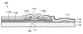
図12は、エッチストッパ型のTFT105を備えた従来のアクティブマトリクス基板120の断面図である。
FIG. 12 is a cross-sectional view of a conventional
このアクティブマトリクス基板120は、以下に説明するように、5枚のフォトマスクを用いて製造することができる。
The
まず、絶縁基板110上に金属膜を成膜した後に、その金属膜を第1のフォトマスクを用いてパターニングして、ゲート電極111を形成する。
First, after forming a metal film over the
続いて、ゲート電極111を覆うように、ゲート絶縁膜112、真性アモルファスシリコン層113aとなる真性アモルファスシリコン膜、及びチャネル保護層114となる無機絶縁膜を順に成膜した後に、その無機絶縁膜を第2のフォトマスクを用いてパターニングして、チャネル保護層114を形成する。
Subsequently, a gate
そして、チャネル保護層114を覆うように、N+アモルファスシリコン層113bとなるN+アモルファスシリコン膜、並びにソース電極115a及びドレイン電極115bとなる金属膜を順に成膜した後に、その金属膜、その下層のN+アモルファスシリコン膜、及びその下層の真性アモルファスシリコン膜を第3のフォトマスクを用いてパターニングして、真性アモルファスシリコン層113a、N+アモルファスシリコン層113b、ソース電極115a及びドレイン電極115bを形成する。
Then, an N + amorphous silicon film to be the N +
さらに、ソース電極115a及びドレイン電極115bを覆うように、層間絶縁膜116となる無機絶縁膜を成膜した後に、その無機絶縁膜を第4のフォトマスクを用いてパターニングして、コンタクトホールを有する層間絶縁膜116を形成する。
Further, after forming an inorganic insulating film to be the
最後に、層間絶縁膜116を覆うように、画素電極117となる透明導電膜を成膜した後に、その透明導電膜を第5のフォトマスクを用いてパターニングして、画素電極117を形成する。
Finally, after forming a transparent conductive film to be the
このアクティブマトリクス基板120では、製造コストを抑制する観点から、フォトマスクの枚数を5枚に削減しているために、チャネル保護層114、ソース電極115a及びドレイン電極115bをマスクとして、N+アモルファスシリコン膜及び真性アモルファスシリコン膜をエッチングするので、真性アモルファスシリコン層113aの周端の側面がソース電極115a及びドレイン電極115bから露出している。
In this
ところで、アモルファスシリコンの半導体層を用いた従来のTFTに代わって、近年、酸化物半導体の半導体層を用いたTFTが提案されている。 By the way, instead of the conventional TFT using an amorphous silicon semiconductor layer, in recent years, a TFT using an oxide semiconductor semiconductor layer has been proposed.
そして、上述した5枚のフォトマスクを用いた製造方法に基づいて、酸化物半導体の半導体層を用いた(TFTを備えた)アクティブマトリクス基板を製造する場合には、酸素欠陥によりキャリア電子が多く発生し易い酸化物半導体の半導体層の周端の側面が、アモルファスシリコンの半導体層を用いたアクティブマトリクス基板120と同様に、ソース電極及びドレイン電極から露出してしまうので、ソース電極及びドレイン電極を形成する際のエッチングや層間絶縁膜を形成する際のCVD(Chemical Vapor Deposition)において半導体層がダメージを受けたりして、TFTの特性が低下するおそれがある。
When an active matrix substrate using an oxide semiconductor layer (comprising a TFT) is manufactured based on the above-described manufacturing method using five photomasks, there are many carrier electrons due to oxygen defects. Like the
本発明は、かかる点に鑑みてなされたものであり、その目的とするところは、フォトマスクの枚数を増やすことなく、酸化物半導体の半導体層を用いた薄膜トランジスタの特性の低下を抑制することにある。 The present invention has been made in view of the above points, and an object of the present invention is to suppress deterioration in characteristics of a thin film transistor using an oxide semiconductor layer without increasing the number of photomasks. is there.
上記目的を達成するために、本発明は、ソース電極及びドレイン電極と酸化物半導体層との間に酸化物半導体層を覆うように保護絶縁膜を設けるようにしたものである。 In order to achieve the above object, according to the present invention, a protective insulating film is provided between a source electrode and a drain electrode and an oxide semiconductor layer so as to cover the oxide semiconductor layer.
具体的に本発明に係るアクティブマトリクス基板は、マトリクス状に設けられた複数の画素電極と、上記各画素電極にそれぞれ接続された複数の薄膜トランジスタと、互いに平行に延びるように設けられた複数のソース線とを備え、上記各薄膜トランジスタが、絶縁基板に設けられたゲート電極と、該ゲート電極を覆うように設けられたゲート絶縁膜と、該ゲート絶縁膜上に上記ゲート電極に重なるように設けられた酸化物半導体層と、互いに対峙するように設けられ、該酸化物半導体層にそれぞれ接続されたソース電極及びドレイン電極とを備えたアクティブマトリクス基板であって、上記ソース電極及びドレイン電極と上記酸化物半導体層との間には、該酸化物半導体層を覆うように保護絶縁膜が設けられ、上記各ソース線は、金属材料により形成され、上記ソース電極及びドレイン電極は、上記各画素電極と同一材料により形成されていることを特徴とする。 Specifically, an active matrix substrate according to the present invention includes a plurality of pixel electrodes provided in a matrix, a plurality of thin film transistors connected to each of the pixel electrodes, and a plurality of sources provided so as to extend in parallel to each other. Each thin film transistor includes a gate electrode provided on an insulating substrate, a gate insulating film provided so as to cover the gate electrode, and a gate insulating film overlying the gate electrode. An active matrix substrate provided with an oxide semiconductor layer and a source electrode and a drain electrode provided so as to face each other and connected to the oxide semiconductor layer, respectively, wherein the source electrode and the drain electrode and the oxidation electrode are provided A protective insulating film is provided between the oxide semiconductor layer so as to cover the oxide semiconductor layer, and each of the source lines is formed of a metal material. Be more formed, the source electrode and the drain electrode, characterized in that it is formed of the same material as said pixel electrode.
上記の構成によれば、各薄膜トランジスタにおいて、ソース電極及びドレイン電極と酸化物半導体層との間に酸化物半導体層を覆うように保護絶縁膜が設けられているので、例えば、ソース電極(、ソース電極に接続するソース線)及びドレイン電極を形成するために、導電膜をエッチングによりパターニングする際に、並びに各画素電極の下層となる層間絶縁膜を形成するために、無機絶縁膜をCVDにより成膜する際に、酸化物半導体層が表面に露出しないことになる。そのため、酸化物半導体層がエッチングやCVDでダメージを受け難くなるので、薄膜トランジスタの特性の低下が抑制される。また、上記構成のアクティブマトリクス基板は、第1のフォトマスクを用いてゲート電極を形成し、第2のフォトマスクを用いて酸化物半導体層を形成し、(場合によっては第3のフォトマスクを用いて、ソース電極に接続するソース線を形成し、)第3(又は第4)のフォトマスクを用いて保護絶縁膜を形成し、第4(又は第5)のフォトマスクを用いて画素電極、ソース電極及びドレイン電極を形成するので、計4枚(又は5枚)のフォトマスクを用いて製造される。したがって、フォトマスクの枚数を増やすことなく、酸化物半導体の半導体層を用いた薄膜トランジスタの特性の低下が抑制される。 According to the above configuration, in each thin film transistor, the protective insulating film is provided so as to cover the oxide semiconductor layer between the source and drain electrodes and the oxide semiconductor layer. In order to form a source line and a drain electrode connected to the electrode, when patterning the conductive film by etching, and to form an interlayer insulating film to be a lower layer of each pixel electrode, the inorganic insulating film is formed by CVD. When the film is formed, the oxide semiconductor layer is not exposed to the surface. Therefore, the oxide semiconductor layer is hardly damaged by etching or CVD, so that deterioration in characteristics of the thin film transistor is suppressed. In the active matrix substrate having the above structure, a gate electrode is formed using a first photomask, an oxide semiconductor layer is formed using a second photomask, and a third photomask may be used in some cases. A source line connected to the source electrode is formed, a protective insulating film is formed using a third (or fourth) photomask, and a pixel electrode is formed using the fourth (or fifth) photomask. Since the source electrode and the drain electrode are formed, it is manufactured using a total of four (or five) photomasks. Accordingly, deterioration in characteristics of a thin film transistor using an oxide semiconductor layer is suppressed without increasing the number of photomasks.
上記ドレイン電極は、上記各画素電極と一体に形成され、上記ソース電極は、上記各画素電極と同一層に形成されていてもよい。 The drain electrode may be formed integrally with each pixel electrode, and the source electrode may be formed in the same layer as each pixel electrode.
上記の構成によれば、ドレイン電極が各画素電極と一体に形成され、ソース電極が各画素電極と同一層に同一材料により形成されているので、各画素電極、ソース電極及びドレイン電極が、透明導電膜などの導電膜をパターニングして形成される。 According to the above configuration, since the drain electrode is formed integrally with each pixel electrode and the source electrode is formed of the same material in the same layer as each pixel electrode, each pixel electrode, source electrode and drain electrode are transparent. It is formed by patterning a conductive film such as a conductive film.
上記各ソース線と交差する方向に互いに平行に延びるように設けられた複数のゲート線を備え、上記各ゲート線と上記各ソース線との交差部分には、上記ゲート絶縁膜及び保護絶縁膜が配置されていてもよい。 A plurality of gate lines provided so as to extend in parallel with each other in a direction intersecting with the source lines, and the gate insulating film and the protective insulating film are provided at the intersections of the gate lines and the source lines; It may be arranged.
上記の構成によれば、各ゲート線と各ソース線との交差部分にゲート絶縁膜及び保護絶縁膜が配置されているので、各ゲート線と各ソース線との交差部分に配置される絶縁膜が厚膜化され、ソース−ゲート間の容量が低減されると共に、ソース−ゲート間の短絡が抑制される。 According to the above configuration, since the gate insulating film and the protective insulating film are disposed at the intersections between the gate lines and the source lines, the insulating films disposed at the intersections between the gate lines and the source lines. Thus, the source-gate capacitance is reduced, and the source-gate short circuit is suppressed.
上記保護絶縁膜は、塗布型の絶縁膜であってもよい。 The protective insulating film may be a coating type insulating film.
上記の構成によれば、保護絶縁膜が比較的厚く形成され易い塗布型の絶縁膜であるので、ソース−ゲート間の容量がいっそう低減されると共に、ソース−ゲート間の短絡がいっそう抑制される。 According to the above configuration, since the protective insulating film is a coating-type insulating film that is easily formed relatively thick, the source-gate capacitance is further reduced and the source-gate short circuit is further suppressed. .
上記各画素電極と上記保護絶縁膜との間には、層間絶縁膜が設けられていてもよい。 An interlayer insulating film may be provided between each of the pixel electrodes and the protective insulating film.
上記構成によれば、各画素電極と保護絶縁膜との間に層間絶縁膜が設けられているので、例えば、ソース線を層間絶縁膜で被覆して保護することが可能になる。 According to the above configuration, since the interlayer insulating film is provided between each pixel electrode and the protective insulating film, for example, the source line can be covered and protected by the interlayer insulating film.
また、本発明に係る表示パネルは、互いに対向するように設けられたアクティブマトリクス基板及び対向基板と、上記アクティブマトリクス基板及び対向基板の間に設けられた表示媒体層とを備えた表示パネルであって、上記アクティブマトリクス基板は、マトリクス状に設けられた複数の画素電極と、上記各画素電極にそれぞれ接続された複数の薄膜トランジスタと、互いに平行に延びるように設けられた複数のソース線とを備え、上記各薄膜トランジスタが、絶縁基板に設けられたゲート電極と、該ゲート電極を覆うように設けられたゲート絶縁膜と、該ゲート絶縁膜上に上記ゲート電極に重なるように設けられた酸化物半導体層と、互いに対峙するように設けられ、該酸化物半導体層にそれぞれ接続されたソース電極及びドレイン電極とを備え、上記ソース電極及びドレイン電極と上記酸化物半導体層との間には、該酸化物半導体層を覆うように保護絶縁膜が設けられ、上記各ソース線は、金属材料により形成され、上記ソース電極及びドレイン電極は、上記各画素電極と同一材料により形成されていることを特徴とする。 The display panel according to the present invention is a display panel including an active matrix substrate and a counter substrate provided so as to face each other, and a display medium layer provided between the active matrix substrate and the counter substrate. The active matrix substrate includes a plurality of pixel electrodes provided in a matrix, a plurality of thin film transistors respectively connected to the pixel electrodes, and a plurality of source lines provided to extend in parallel to each other. Each of the thin film transistors includes a gate electrode provided on an insulating substrate, a gate insulating film provided so as to cover the gate electrode, and an oxide semiconductor provided on the gate insulating film so as to overlap the gate electrode And a source electrode and a drain electrode which are provided so as to face each other and which are respectively connected to the oxide semiconductor layer A protective insulating film is provided between the source and drain electrodes and the oxide semiconductor layer so as to cover the oxide semiconductor layer, and each of the source lines is formed of a metal material, The source electrode and the drain electrode are formed of the same material as each of the pixel electrodes.
上記の構成によれば、各薄膜トランジスタにおいて、ソース電極及びドレイン電極と酸化物半導体層との間に酸化物半導体層を覆うように保護絶縁膜が設けられているので、例えば、ソース電極(、ソース電極に接続するソース線)及びドレイン電極を形成するために、導電膜をエッチングによりパターニングする際に、並びに各画素電極の下層となる層間絶縁膜を形成するために、無機絶縁膜をCVDにより成膜する際に、酸化物半導体層が表面に露出しないことになる。そのため、酸化物半導体層がエッチングやCVDでダメージを受け難くなるので、薄膜トランジスタの特性の低下が抑制される。また、上記構成のアクティブマトリクス基板は、第1のフォトマスクを用いてゲート電極を形成し、第2のフォトマスクを用いて酸化物半導体層を形成し、(場合によっては第3のフォトマスクを用いて、ソース電極に接続するソース線を形成し、)第3(又は第4)のフォトマスクを用いて保護絶縁膜を形成し、第4(又は第5)のフォトマスクを用いて画素電極、ソース電極及びドレイン電極を形成するので、計4枚(又は5枚)のフォトマスクを用いて製造される。したがって、互いに対向するように設けられたアクティブマトリクス基板及び対向基板と、それらの両基板の間に設けられた表示媒体層とを備えた表示パネルにおいて、フォトマスクの枚数を増やすことなく、酸化物半導体の半導体層を用いた薄膜トランジスタの特性の低下が抑制される。 According to the above configuration, in each thin film transistor, the protective insulating film is provided so as to cover the oxide semiconductor layer between the source and drain electrodes and the oxide semiconductor layer. In order to form a source line and a drain electrode connected to the electrode, when patterning the conductive film by etching, and to form an interlayer insulating film to be a lower layer of each pixel electrode, the inorganic insulating film is formed by CVD. When the film is formed, the oxide semiconductor layer is not exposed to the surface. Therefore, the oxide semiconductor layer is hardly damaged by etching or CVD, so that deterioration in characteristics of the thin film transistor is suppressed. In the active matrix substrate having the above structure, a gate electrode is formed using a first photomask, an oxide semiconductor layer is formed using a second photomask, and a third photomask may be used in some cases. A source line connected to the source electrode is formed, a protective insulating film is formed using a third (or fourth) photomask, and a pixel electrode is formed using the fourth (or fifth) photomask. Since the source electrode and the drain electrode are formed, it is manufactured using a total of four (or five) photomasks. Accordingly, in a display panel including an active matrix substrate and a counter substrate provided to face each other, and a display medium layer provided between the two substrates, the oxide can be formed without increasing the number of photomasks. Degradation of the characteristics of the thin film transistor using the semiconductor layer of the semiconductor is suppressed.
本発明によれば、ソース電極及びドレイン電極と酸化物半導体層との間に酸化物半導体層を覆うように保護絶縁膜が設けられているので、フォトマスクの枚数を増やすことなく、酸化物半導体の半導体層を用いた薄膜トランジスタの特性の低下を抑制することができる。 According to the present invention, since the protective insulating film is provided so as to cover the oxide semiconductor layer between the source and drain electrodes and the oxide semiconductor layer, the oxide semiconductor can be formed without increasing the number of photomasks. The deterioration of the characteristics of the thin film transistor using this semiconductor layer can be suppressed.
以下、本発明の実施形態を図面に基づいて詳細に説明する。なお、本発明は、以下の各実施形態に限定されるものではない。 Hereinafter, embodiments of the present invention will be described in detail with reference to the drawings. The present invention is not limited to the following embodiments.
《発明の実施形態1》
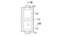
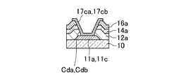
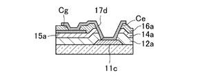
図1〜図9は、本発明に係るアクティブマトリクス基板及びそれを備えた表示パネル、並びにアクティブマトリクス基板の製造方法の実施形態1を示している。具体的に図1は、本実施形態の液晶表示パネル50の断面図である。また、図2は、液晶表示パネル50を構成するアクティブマトリクス20aの各画素を示す平面図であり、図3は、そのゲート端子17caが形成された部分の平面図であり、図4は、そのソース端子17cbが形成された部分の平面図であり、図5は、そのゲートソース接続部17dが形成された部分の平面図である。さらに、図6は、図2中のVI−VI線に沿ったアクティブマトリクス基板20aの画素部の断面図であり、図7は、図3及び図4のVII−VII線に沿ったアクティブマトリクス基板20aのゲート端子17ca及びソース端子17cbが形成された部分の断面図であり、図8は、図5中のVIII−VIII線に沿ったアクティブマトリクス20aのゲートソース接続部17dが形成された部分の断面図である。
Embodiment 1 of the Invention
1 to 9 show Embodiment 1 of an active matrix substrate, a display panel including the same, and a method for manufacturing the active matrix substrate according to the present invention. Specifically, FIG. 1 is a cross-sectional view of the liquid
液晶表示パネル50は、図1に示すように、互いに対向するように設けられたアクティブマトリクス基板20a及び対向基板30と、アクティブマトリクス基板20a及び対向基板30の間に表示媒体層として設けられた液晶層40と、アクティブマトリクス基板20a及び対向基板30を互いに接着すると共にアクティブマトリクス基板20a及び対向基板30の間に液晶層40を封入するために枠状に設けられたシール材35とを備えている。
As shown in FIG. 1, the liquid
アクティブマトリクス基板20aは、図2及び図6に示すように、絶縁基板10上に互いに平行に延びるように設けられた複数のゲート線11aと、各ゲート線11aの間にそれぞれ設けられ、互いに平行に延びる複数の容量線11bと、各ゲート線11aと直交する方向に互いに平行に延びるように設けられた複数のソース線15aと、各ゲート線11a及び各ソース線15aの交差部分毎、すなわち、各画素毎にそれぞれ設けられた複数のTFT5と、マトリクス状に設けられ、各TFT5にそれぞれ接続された複数の画素電極Pと、各画素電極Pを覆うように設けられた配向膜(不図示)とを備え、Cs on Common構造になっている。
As shown in FIGS. 2 and 6, the
ゲート線11aは、画像表示を行う表示領域D(図1参照)の外側の端子領域T(図1参照)に引き出され、その端子領域Tにおいて、図3及び図7に示すように、ゲート絶縁膜12a、保護絶縁膜14a及び層間絶縁膜16aの積層膜に形成されたコンタクトホールCdaを介してゲート端子17caに接続されている。
The
ソース線15aは、表示領域D(図1参照)の外側に引き出され、図5及び図8に示すように、層間絶縁膜16aに形成されたコンタクトホールCgを介してゲートソース接続部17dに接続され、そのゲートソース接続部17dがゲート絶縁膜12a、保護絶縁膜14a及び層間絶縁膜16aの積層膜に形成されたコンタクトホールCeを介して中継配線11cに接続され、図4及び図7に示すように、その中継配線11cが端子領域Tにおいてゲート絶縁膜12a、保護絶縁膜14a及び層間絶縁膜16aの積層膜に形成されたコンタクトホールCdbを介してソース端子17cbに接続されている。
The
TFT5は、図2及び図6に示すように、絶縁基板10上に設けられたゲート電極(11a)と、ゲート電極(11a)を覆うように設けられたゲート絶縁膜12aと、ゲート絶縁膜12a上でゲート電極(11a)に対応する位置に島状に設けられた酸化物半導体層13aと、酸化物半導体層13aの上層側で互いに対峙するように設けられ、酸化物半導体層13aに接続されたソース電極17a及びドレイン電極17bとを備えている。ここで、ソース電極17a及びドレイン電極17bと酸化物半導体層13aとの間には、図6に示すように、酸化物半導体層13aのソース電極17a及びドレイン電極17bとの接続部分以外を覆うように設けられた保護絶縁膜14aが設けられている。そして、ゲート電極(11a)は、図2に示すように、ゲート線11aの一部である。また、ソース電極17aは、図2及び図6に示すように、保護絶縁膜14a及び層間絶縁膜16aの積層膜に形成されたコンタクトホールCaを介して酸化物半導体層13aに接続されていると共に、層間絶縁膜16aに形成されたコンタクトホールCfを介してソース線15aに接続されている。また、ドレイン電極17bは、図2及び図5に示すように、保護絶縁膜14a及び層間絶縁膜16aの積層膜に形成されたコンタクトホールCbを介して酸化物半導体層13aに接続されていると共に、隣り合う一対のゲート線11a及び隣り合う一対のソース線15aに囲まれた画素領域に延設されて画素電極Pを構成している。さらに、ドレイン電極17bは、図2及び図6に示すように、保護絶縁膜14a及び層間絶縁膜16aの積層膜に形成されたコンタクトホールCcを介して容量電極13bに接続され、その容量電極13bがゲート絶縁膜12aを介して容量線11bに重なることにより、補助容量を構成している。また、酸化物半導体層13aは、例えば、IGZO(In-Ga-Zn-O)系、ISiZO(In-Si-Zn-O)系、IAlZO(In-Al-Zn-O)系などの酸化物半導体膜により形成されている。
2 and 6, the
対向基板30は、絶縁基板上に格子状に設けられたブラックマトリクス(不図示)並びにそのブラックマトリクスの各格子間にそれぞれ設けられた赤色層、緑色層及び青色層などの着色層(不図示)を有するカラーフィルター層(不図示)と、そのカラーフィルター層を覆うように設けられた共通電極(不図示)と、その共通電極上に設けられたフォトスペーサ(不図示)と、その共通電極を覆うように設けられた配向膜(不図示)とを備えている。
The
液晶層40は、電気光学特性を有するネマチックの液晶材料などにより構成されている。
The
上記構成の液晶表示パネル50では、各画素において、ゲートドライバ(不図示)からゲート信号がゲート線11aを介してゲート電極(11a)に送られて、TFT5がオン状態になったときに、ソースドライバ(不図示)からソース信号がソース線15aを介してソース電極17aに送られて、酸化物半導体層13a及びドレイン電極17bを介して、画素電極Pに所定の電荷が書き込まれる。このとき、アクティブマトリクス基板20aの各画素電極Pと対向基板30の共通電極との間において電位差が生じ、液晶層40、すなわち、各画素の液晶容量及びその液晶容量に並列に接続された補助容量に所定の電圧が印加される。そして、液晶表示パネル50では、各画素において、液晶層40に印加する電圧の大きさによって液晶層40の配向状態を変えることにより、液晶層40の光透過率を調整して画像が表示される。
In the liquid
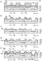
次に、本実施形態の液晶表示パネル50の製造方法の一例について図9を用いて説明する。ここで、図9は、アクティブマトリクス基板20aの製造工程を示す断面図である。なお、本実施形態の製造方法は、アクティブマトリクス基板作製工程、対向基板作製工程及び液晶注入工程を備える。
Next, an example of the manufacturing method of the liquid
<アクティブマトリクス基板作製工程>
まず、ガラス基板などの絶縁基板10の基板全体に、スパッタリング法により、例えば、チタン膜(厚さ50nm程度)、アルミニウム膜(厚さ200nm程度)及びチタン膜(厚さ100nm程度)などを順に積層した第1の金属膜を成膜し、その後、第1のフォトマスクを用いたフォトリソグラフィ、第1の金属膜のドライエッチング、レジストの剥離、及び洗浄を行うことにより、図9(a)に示すように、ゲート線(ゲート電極)11a、容量線11b及び中継配線11cを形成する(ゲート電極形成工程)。
<Active matrix substrate manufacturing process>
First, for example, a titanium film (thickness of about 50 nm), an aluminum film (thickness of about 200 nm), a titanium film (thickness of about 100 nm), and the like are sequentially laminated on the entire substrate of the insulating
続いて、ゲート線(ゲート電極)11a、容量線11b及び中継配線11cが形成された基板全体に、CVD(Chemical Vapor Deposition)法により、例えば、酸化シリコン膜(厚さ200nm〜500nm程度)などの無機絶縁膜12を成膜した後に、スパッタリング法により、例えば、IGZO系の酸化物半導体膜(厚さ30nm〜300nm程度)を成膜し、その後、第2のフォトマスクを用いたフォトリソグラフィ、酸化物半導体膜のウエットエッチング、レジストの剥離、及び洗浄を行うことにより、図9(b)に示すように、酸化物半導体層13a及び容量電極13bを形成する(半導体層形成工程)。なお、本実施形態では、単層の無機絶縁膜12を例示したが、例えば、下層が窒化シリコン膜(厚さ200nm〜500nm程度)により構成され、上層が酸化シリコン膜(例えば、20nm〜150nm程度)により構成された複層の無機第絶縁膜12であってもよい。
Subsequently, for example, a silicon oxide film (thickness of about 200 nm to 500 nm) is formed on the entire substrate on which the gate line (gate electrode) 11a, the
さらに、酸化物半導体層13a及び容量電極13bが形成された基板全体に、CVD法により、図9(c)に示すように、例えば、酸化シリコン膜(厚さ50nm〜200nm程度)などの第1の無機絶縁膜(絶縁材料膜)14を成膜した後に、スパッタリング法により、例えば、チタン膜(厚さ50nm程度)、アルミニウム膜(厚さ200nm程度)及びチタン膜(厚さ100nm程度)などを順に積層した第2の金属膜15を成膜する。その後、第3のフォトマスクを用いたフォトリソグラフィ、第2の金属膜15のドライエッチング、レジストの剥離、及び洗浄を行うことにより、図9(d)に示すように、ソース線15aを形成する。なお、本実施形態では、単層の第1の無機絶縁膜14を例示したが、例えば、下層が酸化シリコン膜により構成され、上層が窒化シリコン膜により構成された複層の第1の無機絶縁膜14であってもよい。
Furthermore, as shown in FIG. 9C, the first substrate such as a silicon oxide film (having a thickness of about 50 nm to 200 nm) is formed on the entire substrate on which the
そして、ソース線15aが形成された基板全体に、CVD法により、例えば、酸化シリコン膜(厚さ50nm〜300nm程度)などの第2の無機絶縁膜(他の絶縁材料膜)16を成膜した後に、第4のフォトマスクを用いたフォトリソグラフィ、第2の無機絶縁膜16のウエットエッチング、第1の無機絶縁膜14及び第2の無機絶縁膜16の積層膜のウエットエッチング、並びに無機絶縁膜12、第1の無機絶縁膜14及び第2の無機絶縁膜16の積層膜のウエットエッチング、レジストの剥離、及び洗浄を行うことにより、図9(e)に示すように、コンタクトホールCa、Cb、Cc、Cda、Cdb、Ce(図8参照)、Cf及びCg(図8参照)を形成して、ゲート絶縁膜12a、保護絶縁膜14a及び層間絶縁膜16aを形成する(保護絶縁膜形成工程)。なお、本実施形態では、単層の第2の無機絶縁膜16を例示したが、例えば、下層が酸化シリコン膜により構成され、上層が窒化シリコン膜により構成された複層の第2の無機絶縁膜16であってもよい。
Then, a second inorganic insulating film (another insulating material film) 16 such as a silicon oxide film (thickness of about 50 nm to 300 nm) is formed on the entire substrate on which the
さらに、ゲート絶縁膜12a、保護絶縁膜14a及び層間絶縁膜16aが形成された基板全体に、スパッタリング法により、例えば、ITO(Indium Tin Oxide、厚さ100nm程度)などの透明導電膜17を成膜し、その後、第5のフォトマスクを用いたフォトリソグラフィ、透明導電膜17のドライエッチング、レジストの剥離、及び洗浄を行うことにより、図9(f)に示すように、ソース電極17a、ドレイン電極17b(画素電極P)、ゲート端子17ca、ソース端子17cb及びゲートソース接続部17d(図8参照)を形成する(画素電極形成工程)。
Further, a transparent
最後に、ソース電極17a、ドレイン電極17b(画素電極P)、ゲート端子17ca、ソース端子17cb及びゲートソース接続部17dが形成された基板全体に、印刷法によりポリイミド樹脂を塗布し、その後、ラビング処理を行うことにより、配向膜を厚さ100nm程度に形成する。
Finally, polyimide resin is applied to the entire substrate on which the
以上のようにして、アクティブマトリクス基板20aを作製することができる。
As described above, the
<対向基板作製工程>
まず、ガラス基板などの絶縁基板の基板全体に、スピンコート法により、例えば、カーボンなどの微粒子が分散されたアクリル系の感光性樹脂を塗布し、その塗布された感光性樹脂をフォトマスクを介して露光した後に、現像することにより、ブラックマトリクスを厚さ1.5μm程度に形成する。
<Opposite substrate manufacturing process>
First, an acrylic photosensitive resin in which fine particles such as carbon are dispersed is applied to the entire substrate of an insulating substrate such as a glass substrate by spin coating, for example, and the applied photosensitive resin is passed through a photomask. After the exposure, development is performed to form a black matrix having a thickness of about 1.5 μm.
続いて、上記ブラックマトリクスが形成された基板全体に、スピンコート法により、例えば、赤、緑又は青に着色されたアクリル系の感光性樹脂を塗布し、その塗布された感光性樹脂をフォトマスクを介して露光した後に、現像することによりパターニングして、選択した色の着色層(例えば、赤色層)を厚さ2.0μm程度に形成する。さらに、他の2色についても同様な工程を繰り返して、他の2色の着色層(例えば、緑色層及び青色層)を厚さ2.0μm程度に形成して、カラーフィルター層を形成する。 Subsequently, for example, an acrylic photosensitive resin colored in red, green, or blue is applied to the entire substrate on which the black matrix is formed by a spin coating method, and the applied photosensitive resin is applied to a photomask. After being exposed to light, patterning is performed by developing to form a colored layer (for example, a red layer) of a selected color with a thickness of about 2.0 μm. Further, the same process is repeated for the other two colors to form other two colored layers (for example, a green layer and a blue layer) with a thickness of about 2.0 μm to form a color filter layer.
さらに、上記カラーフィルター層が形成された基板上に、スパッタリング法により、例えば、ITOなどの透明導電膜を成膜して、共通電極を厚さ100nm程度に形成する。 Further, a transparent conductive film such as, for example, ITO is formed on the substrate on which the color filter layer is formed by a sputtering method to form a common electrode with a thickness of about 100 nm.
その後、上記共通電極が形成された基板全体に、スピンコート法により、感光性樹脂を塗布し、その塗布された感光性樹脂をフォトマスクを介して露光した後に、現像することにより、フォトスペーサを厚さ4μm程度に形成する。 Thereafter, a photosensitive resin is applied to the entire substrate on which the common electrode is formed by a spin coating method, and the applied photosensitive resin is exposed through a photomask and then developed, thereby developing a photo spacer. It is formed to a thickness of about 4 μm.
最後に、上記フォトスペーサが形成された基板全体に、印刷法によりポリイミド系樹脂を塗布し、その後、ラビング処理を行うことにより、配向膜を厚さ100nm程度に形成する。 Finally, a polyimide resin is applied to the entire substrate on which the photo spacers are formed by a printing method, and then a rubbing process is performed to form an alignment film with a thickness of about 100 nm.
以上のようにして、対向基板30を作製することができる。
The
<液晶注入工程>
まず、例えば、ディスペンサを用いて、上記対向基板作製工程で作製された対向基板30に、紫外線硬化及び熱硬化併用型樹脂などにより構成されたシール材35を枠状に描画する。
<Liquid crystal injection process>
First, for example, using a dispenser, a
続いて、上記シール材が描画された対向基板30におけるシール材35の内側の領域に液晶材料を滴下する。
Subsequently, a liquid crystal material is dropped onto a region inside the sealing
さらに、上記液晶材料が滴下された対向基板30と、上記アクティブマトリクス基板作製工程で作製されたアクティブマトリクス基板20aとを、減圧下で貼り合わせた後に、その貼り合わせた貼合体を大気圧に開放することにより、その貼合体の表面及び裏面を加圧する。
Further, after the
最後に、上記貼合体に挟持されたシール材35にUV光を照射した後に、その貼合体を加熱することによりシール材35を硬化させる。
Finally, after irradiating the sealing
以上のようにして、本実施形態の液晶表示パネル50を製造することができる。
As described above, the liquid
以上説明したように、本実施形態のアクティブマトリクス基板20a及びそれを備えた液晶表示パネル50、並びにアクティブマトリクス基板20aの製造方法によれば、保護絶縁膜形成工程において、半導体層形成工程で形成された酸化物半導体層13aを覆うように、第1の無機絶縁膜14を成膜した後に、その第1の無機絶縁膜14をパターニングして、酸化物半導体層13aのソース電極17a及びドレイン電極17bとの接続部分が開口した保護絶縁膜14aを形成するので、画素電極形成工程において、各画素電極P、ソース電極17a及びドレイン電極17bを形成するために、透明導電膜17をエッチングによりパターニングする際に、酸化物半導体層13aが表面に露出しないことになる。そのため、酸化物半導体層13aがエッチングでダメージを受け難くなるので、TFT5の特性の低下を抑制することができる。また、保護絶縁膜形成工程において、第1の無機絶縁膜14を覆うように第2の金属膜15を成膜し、その第2の金属膜15をパターニングして、ソース線15aを形成した後に、第1の無機絶縁膜14をパターニングして、保護絶縁膜14aを形成するので、第2の金属膜15をエッチングによりパターニングして、ソース線15aを形成する際に、酸化物半導体層13aが第1の無機絶縁膜14で覆われていることになり、酸化物半導体層13aが第2の金属膜15のエッチングでダメージを受け難くなる。さらに、保護絶縁膜形成工程において、第1の無機絶縁膜14を覆うように第2の無機絶縁膜16を成膜し、第1の無機絶縁膜14及び第2の無機絶縁膜16の積層膜をパターニングして、第1の無機絶縁膜14により保護絶縁膜14aを形成すると共に、第2の無機絶縁膜16により層間絶縁膜16aを形成するので、第2の無機絶縁膜16をCVDにより成膜する際に、酸化物半導体層13aが第1の無機絶縁膜14で覆われていることになり、酸化物半導体層13aが第2の無機絶縁膜16のCVDでダメージを受け難くなる。また、アクティブマトリクス基板20aは、ゲート電極形成工程で第1のフォトマスクを用い、半導体層形成工程で第2のフォトマスクを用い、保護絶縁膜形成工程で第3及び第4のフォトマスクを用い、画素電極形成工程で第5のフォトマスクを用いるので、計5枚のフォトマスクを用いて製造される。したがって、アクティブマトリクス基板20a及びそれを備えた液晶表示パネル50において、フォトマスクの枚数を増やすことなく、酸化物半導体の半導体層を用いたTFTの特性の低下を抑制することができる。
As described above, according to the
また、本実施形態のアクティブマトリクス基板20aによれば、ドレイン電極17bが各画素電極Pと一体に形成され、ソース電極17aが各画素電極Pと同一層に同一材料により形成されているので、各画素電極P、ソース電極17a及びドレイン電極17bを、透明導電膜17などの導電膜をパターニングして形成することができる。
Further, according to the
また、本実施形態のアクティブマトリクス基板20aによれば、各ゲート線11aと各ソース線15aとの交差部分にゲート絶縁膜12a及び保護絶縁膜14aが配置されているので、各ゲート線11aと各ソース線15aとの交差部分に配置される絶縁膜が厚膜化され、ソース−ゲート間の容量を低減することができると共に、ソース−ゲート間の短絡を抑制することができる。
Further, according to the
なお、本実施形態では、5枚のフォトマスクを用いるアクティブマトリクス基板20aの製造方法を例示したが、第2の金属膜15の成膜及びそのパターニングを省略して、金属膜15に形成されていたソース線(15a)を、各画素電極Pと同一層に同一材料(透明導電膜17)により形成することにより、4枚のフォトマスクを用いてアクティブマトリクス基板を製造することができる。
In the present embodiment, the manufacturing method of the
《発明の実施形態2》
図10は、本実施形態の液晶表示パネルを構成するアクティブマトリクス基板20bの製造工程を示す説明図である。なお、以下の各実施形態において、図1〜図9と同じ部分については同じ符号を付して、その詳細な説明を省略する。
<< Embodiment 2 of the Invention >>
FIG. 10 is an explanatory view showing a manufacturing process of the
本実施形態の液晶表示パネルは、互いに対向するように設けられたアクティブマトリクス基板20b及び対向基板30(図1参照)と、アクティブマトリクス基板20b及び対向基板30の間に設けられた液晶層40(図1参照)とを備えている。
The liquid crystal display panel of this embodiment includes an
アクティブマトリクス基板20bでは、TFT5が、図10(e)に示すように、絶縁基板10上に設けられたゲート電極(11a)と、ゲート電極(11a)を覆うように設けられたゲート絶縁膜12bと、ゲート絶縁膜12b上でゲート電極(11a)に対応する位置に島状に設けられた酸化物半導体層13aと、酸化物半導体層13aの上層側で互いに対峙するように設けられ、酸化物半導体層13aに接続されたソース電極17a及びドレイン電極17bとを備えている。ここで、ソース電極17a及びドレイン電極17bと酸化物半導体層13aとの間には、図10(e)に示すように、酸化物半導体層13aのソース電極17a及びドレイン電極17bとの接続部分以外を覆うように設けられた保護絶縁膜14bが設けられている。また、ソース電極17aは、図10(e)に示すように、(保護絶縁膜14b及び)層間絶縁膜16bに形成されたコンタクトホールCaを介して酸化物半導体層13aに接続されていると共に、層間絶縁膜16bに形成されたコンタクトホールCfを介してソース線15aに接続されている。また、ドレイン電極17bは、図10(e)に示すように、(保護絶縁膜14b及び)層間絶縁膜16bに形成されたコンタクトホールCbを介して酸化物半導体層13aに接続されていると共に、画素領域に延設されて画素電極Pを構成している。
In the
次に、本実施形態のアクティブマトリクス基板20bの製造方法の一例について図10を用いて説明する。なお、本実施形態の製造方法は、上記実施形態1のアクティブマトリクス基板作製工程における保護絶縁膜形成工程を変更するだけであるので、保護膜形成工程を中心に説明する。
Next, an example of a method for manufacturing the
まず、上記実施形態1のアクティブマトリクス基板作製工程における半導体層形成工程を行って酸化物半導体層13a及び容量電極13bが形成された基板全体に、CVD法により、図10(a)に示すように、例えば、酸化シリコン膜(厚さ50nm〜200nm程度)などの第1の無機絶縁膜(絶縁材料膜)14を成膜した後に、スパッタリング法により、例えば、チタン膜(厚さ50nm程度)、アルミニウム膜(厚さ200nm程度)及びチタン膜(厚さ100nm程度)などを順に積層した第2の金属膜15を成膜し、さらに、スピンコート法により、感光性樹脂膜Rを塗布し、その塗布された感光性樹脂膜Rをハーフトーンの第3フォトマスクを介して露光した後に、現像することにより、図10(a)に示すように、ソース線15aとなる部分が相対的に厚く、コンタクトホールCa、Cb、Cc、Cda及びCdbなどを形成する部分が開口したレジストパターンRaを形成する。
First, as shown in FIG. 10A, the entire substrate on which the
続いて、レジストパターンRaから露出する第2の金属膜15、及びその下層の第1の無機絶縁膜14、並びにその下層の無機絶縁膜12のドライエッチングを行うことにより、図10(b)に示すように、ゲート絶縁膜12b、保護絶縁膜14b及び金属層15bを形成する。
Subsequently, by performing dry etching on the
さらに、レジストパターンRaをアッシングで薄肉化することにより、図10(b)に示すように、レジストパターンRaの相対的に薄い部分を除去して、レジストパターンRbを形成した後に、レジストパターンRbから露出する金属層15bのドライエッチング、レジストの剥離、及び洗浄を行うことにより、図10(c)に示すように、ソース線15aを形成する。
Further, by thinning the resist pattern Ra by ashing, as shown in FIG. 10B, a relatively thin portion of the resist pattern Ra is removed to form the resist pattern Rb, and then from the resist pattern Rb. By performing dry etching of the exposed
そして、ソース線15aが形成された基板全体に、CVD法により、例えば、酸化シリコン膜(厚さ50nm〜300nm程度)などの第2の無機絶縁膜(他の絶縁材料膜)16を成膜した後に、第4のフォトマスクを用いたフォトリソグラフィ、第2の無機絶縁膜16のウエットエッチング、レジストの剥離、及び洗浄を行うことにより、図10(d)に示すように、層間絶縁膜16bを形成する(保護絶縁膜形成工程)。
Then, a second inorganic insulating film (another insulating material film) 16 such as a silicon oxide film (thickness of about 50 nm to 300 nm) is formed on the entire substrate on which the
さらに、層間絶縁膜16bが形成された基板全体に、スパッタリング法により、例えば、ITO(厚さ100nm程度)などの透明導電膜17を成膜し、その後、第5のフォトマスクを用いたフォトリソグラフィ、透明導電膜17のドライエッチング、レジストの剥離、及び洗浄を行うことにより、図10(e)に示すように、ソース電極17a、ドレイン電極17b(画素電極P)、ゲート端子17ca及びソース端子17cbなどを形成する(画素電極形成工程)。
Further, a transparent
最後に、ソース電極17a、ドレイン電極17b(画素電極P)、ゲート端子17ca及びソース端子17cbなどが形成された基板全体に、印刷法によりポリイミド樹脂を塗布し、その後、ラビング処理を行うことにより、配向膜を厚さ100nm程度に形成する。
Finally, a polyimide resin is applied to the entire substrate on which the
以上のようにして、アクティブマトリクス基板20bを製造することができる。
As described above, the
以上説明したように、本実施形態のアクティブマトリクス基板20b及びそれを備えた液晶表示パネル、並びにアクティブマトリクス基板20aの製造方法によれば、上記実施形態1と同様に、ソース電極17a及びドレイン電極17bと酸化物半導体層13aとの間に酸化物半導体層13aを覆うように保護絶縁膜14bが設けられているので、フォトマスクの枚数を増やすことなく、酸化物半導体の半導体層を用いたTFTの特性の低下を抑制することができる。
As described above, according to the
また、本実施形態のアクティブマトリクス基板20bの製造方法によれば、例えば、透過部、遮光部及び半透過部を備えたハーフトーン(又はグレイトーン)のハーフ露光が可能な1枚のフォトマスクを用いて、ソース線15aを形成する部分が相対的に厚く、酸化物半導体層13aのソース電極17a及びドレイン電極17bとの接続部分が開口したレジストパターンRaを形成し、そのレジストパターンRaを用いて保護絶縁膜14bを形成し、そのレジストパターンRaを薄膜化したレジストパターンRbを用いてソース線15aを形成するので、アクティブマトリクス基板20bの製造コストを低減することができる。
Further, according to the manufacturing method of the
また、本実施形態のアクティブマトリクス基板20bの製造方法によれば、保護絶縁膜形成工程において、保護絶縁膜14b上に形成されたソース線15aを覆うように、第2の無機絶縁膜16を成膜した後に、第2の無機絶縁膜16をパターニングして、層間絶縁膜16bを形成するので、例えば、画素電極形成工程の前にドライエッチングにより形成するコンタクトホールの深さが浅くなり、ドライエッチングに要する時間が短くなると共に、層間絶縁膜16bの表面がダメージを受け難くなる。なお、本実施形態では、層間絶縁膜16aが無機絶縁膜により形成されていたが、層間絶縁膜が有機絶縁膜により形成されている場合には、その層間絶縁膜の表面のダメージをいっそう抑制することができるので、画素電極の下層の表面荒れによるコントラスト低下を抑制することができる。
Further, according to the method for manufacturing the
また、本実施形態のアクティブマトリクス基板20bによれば、各ゲート線11aと各ソース線15aとの交差部分にゲート絶縁膜12b及び保護絶縁膜14bが配置されているので、各ゲート線11aと各ソース線15aとの交差部分に配置される絶縁膜が厚膜化され、ソース−ゲート間の容量を低減することができると共に、ソース−ゲート間の短絡を抑制することができる。
Further, according to the
《発明の実施形態3》
図11(a)は、本実施形態の液晶表示パネルを構成するアクティブマトリクス基板20cの断面図であり、図11(b)は、アクティブマトリクス基板20cの製造工程の一部を示す断面図である。
<< Embodiment 3 of the Invention >>
FIG. 11A is a cross-sectional view of the
上記実施形態1及び2では、保護絶縁膜14a及び14bを構成する絶縁材料膜をCVD法により成膜する方法を例示したが、本実施形態では、保護絶縁膜14cを構成する絶縁材料膜を有機樹脂の塗布及び焼成により成膜する方法を例示する。
In the first and second embodiments, the method of forming the insulating material film that forms the protective insulating
本実施形態の液晶表示パネルは、互いに対向するように設けられたアクティブマトリクス基板20c及び対向基板30(図1参照)と、アクティブマトリクス基板20c及び対向基板30の間に設けられた液晶層40(図1参照)とを備えている。
The liquid crystal display panel of the present embodiment includes an
アクティブマトリクス基板20cでは、TFT5のソース電極17a及びドレイン電極17bと酸化物半導体層13aとの間には、図11(a)に示すように、酸化物半導体層13aのソース電極17a及びドレイン電極17bとの接続部分以外を覆うように設けられた保護絶縁膜14cが設けられている。また、ソース電極17aは、図11(a)に示すように、(保護絶縁膜14c及び)層間絶縁膜16bに形成されたコンタクトホールCaを介して酸化物半導体層13aに接続されていると共に、層間絶縁膜16bに形成されたコンタクトホールCfを介してソース線15aに接続されている。また、ドレイン電極17bは、図11(a)に示すように、(保護絶縁膜14c及び)層間絶縁膜16bに形成されたコンタクトホールCbを介して酸化物半導体層13aに接続されていると共に、画素領域に延設されて画素電極Pを構成している。さらに、保護絶縁膜14cは、その厚さが1.5μm程度であり、上記実施形態1及び2の保護絶縁膜14a及び14bよりも厚い塗布型の絶縁膜である。
In the
本実施形態のアクティブマトリクス基板20cは、上記実施形態2の保護絶縁膜形成工程における第1の無機絶縁膜14の成膜方法を、図11(b)に示すように、酸化物半導体層13a及び容量電極13bが形成された基板全体に、スピンコート法により、アクリル樹脂を厚さ1.5μm程度に塗布した後に、150℃で5分間程度のプリベーク、及び200℃で1時間程度のポストベークを行うことにより、有機絶縁膜14sを成膜する方法に変更することにより、製造することができる。
As shown in FIG. 11B, the
以上説明したように、本実施形態のアクティブマトリクス基板20c及びそれを備えた液晶表示パネル、並びにアクティブマトリクス基板20cの製造方法によれば、上記実施形態1及び2と同様に、ソース電極17a及びドレイン電極17bと酸化物半導体層13aとの間に酸化物半導体層13aを覆うように保護絶縁膜14cが設けられているので、フォトマスクの枚数を増やすことなく、酸化物半導体の半導体層を用いたTFTの特性の低下を抑制することができる。
As described above, according to the
また、本実施形態のアクティブマトリクス基板20cによれば、各ゲート線11aと各ソース線15aとの交差部分にゲート絶縁膜12b及び保護絶縁膜14cが配置されていると共に、保護絶縁膜14cが比較的厚く形成され易い塗布型の絶縁膜であるので、各ゲート線11aと各ソース線15aとの交差部分に配置される絶縁膜が厚膜化され、ソース−ゲート間の容量をいっそう低減することができると共に、ソース−ゲート間の短絡をいっそう抑制することができる。
Further, according to the
なお、上記各実施形態では、保護絶縁膜14a、14b及び14c上に層間絶縁膜16a及び16bが設けられた構成を例示したが、本発明では、保護絶縁膜14a、14b及び14c上の層間絶縁膜16a及び16bを省略してもよい。
In each of the above embodiments, the configuration in which the
また、上記各実施形態では、Cs on Common構造のアクティブマトリクス基板を例示したが、本発明は、Cs on Gate構造のアクティブマトリクス基板にも適用することができる。 In each of the above embodiments, an active matrix substrate having a Cs on Common structure is illustrated, but the present invention can also be applied to an active matrix substrate having a Cs on Gate structure.
また、上記各実施形態では、画素電極に接続されたTFTの電極をドレイン電極としたアクティブマトリクス基板を例示したが、本発明は、画素電極に接続されたTFTの電極をソース電極と呼ぶアクティブマトリクス基板にも適用することができる。 In each of the above embodiments, an active matrix substrate in which the electrode of the TFT connected to the pixel electrode is used as the drain electrode is illustrated. However, the present invention is an active matrix in which the electrode of the TFT connected to the pixel electrode is referred to as a source electrode. It can also be applied to a substrate.
以上説明したように、本発明は、フォトマスクの枚数を増やすことなく、酸化物半導体の半導体層を用いたTFTの特性の低下を抑制することができるので、TFTを備えたアクティブマトリクス駆動方式の液晶表示パネルについて有用である。 As described above, the present invention can suppress the deterioration of characteristics of a TFT using an oxide semiconductor layer without increasing the number of photomasks. This is useful for liquid crystal display panels.
P 画素電極
R 感光性樹脂膜
Ra,Rb レジストパターン
5 TFT
10 絶縁基板
11a ゲート線(ゲート電極)
12a ゲート絶縁膜
13a 酸化物半導体層
14 第1の無機絶縁膜(絶縁材料膜)
14a,14b,14c 保護絶縁膜
15 金属膜
15a ソース線
16 第2の無機絶縁膜(他の絶縁材料膜)
16a 層間絶縁膜
17 透明導電膜
17a ソース電極
17b ドレイン電極
20a,20b,20c アクティブマトリクス基板
30 対向基板
40 液晶層(表示媒体層)
50 液晶表示パネル
P Pixel electrode R Photosensitive resin film Ra, Rb Resist
10 Insulating
12a
14a, 14b, 14c
16a
50 LCD panel
Claims (7)
上記各画素電極にそれぞれ接続された複数の薄膜トランジスタと、
互いに平行に延びるように設けられた複数のソース線とを備え、
上記各薄膜トランジスタが、絶縁基板に設けられたゲート電極と、該ゲート電極を覆うように設けられたゲート絶縁膜と、該ゲート絶縁膜上に上記ゲート電極に重なるように設けられた酸化物半導体層と、互いに対峙するように設けられ、該酸化物半導体層にそれぞれ接続されたソース電極及びドレイン電極とを備えたアクティブマトリクス基板であって、
上記ソース電極及びドレイン電極と上記酸化物半導体層との間には、該酸化物半導体層を覆うように保護絶縁膜が設けられ、
上記各ソース線は、金属材料により形成され、
上記ソース電極及びドレイン電極は、上記各画素電極と同一材料により形成されていることを特徴とするアクティブマトリクス基板。 A plurality of pixel electrodes provided in a matrix;
A plurality of thin film transistors respectively connected to the pixel electrodes;
A plurality of source lines provided to extend in parallel to each other,
Each thin film transistor includes a gate electrode provided on an insulating substrate, a gate insulating film provided so as to cover the gate electrode, and an oxide semiconductor layer provided on the gate insulating film so as to overlap the gate electrode And an active matrix substrate provided with a source electrode and a drain electrode provided to face each other and connected to the oxide semiconductor layer,
A protective insulating film is provided between the source and drain electrodes and the oxide semiconductor layer so as to cover the oxide semiconductor layer,
Each of the source lines is formed of a metal material,
The active matrix substrate, wherein the source electrode and the drain electrode are formed of the same material as each of the pixel electrodes.
上記ドレイン電極は、上記各画素電極と一体に形成され、
上記ソース電極は、上記各画素電極と同一層に形成されていることを特徴とするアクティブマトリクス基板。 The active matrix substrate according to claim 1,
The drain electrode is formed integrally with each pixel electrode,
The active matrix substrate, wherein the source electrode is formed in the same layer as the pixel electrodes.
上記各ソース線と交差する方向に互いに平行に延びるように設けられた複数のゲート線を備え、
上記各ゲート線と上記各ソース線との交差部分には、上記ゲート絶縁膜及び保護絶縁膜が配置されていることを特徴とするアクティブマトリクス基板。 The active matrix substrate according to claim 1 or 2,
A plurality of gate lines provided to extend in parallel with each other in a direction intersecting with each of the source lines;
An active matrix substrate, wherein the gate insulating film and the protective insulating film are arranged at the intersections between the gate lines and the source lines.
上記保護絶縁膜は、塗布型の絶縁膜であることを特徴とするアクティブマトリクス基板。 The active matrix substrate according to claim 3,
An active matrix substrate, wherein the protective insulating film is a coating type insulating film.
上記各画素電極と上記保護絶縁膜との間には、層間絶縁膜が設けられていることを特徴とするアクティブマトリクス基板。 The active matrix substrate according to any one of claims 1 to 4,
An active matrix substrate, wherein an interlayer insulating film is provided between each of the pixel electrodes and the protective insulating film.
上記酸化物半導体層は、In-Ga-Zn-O系であることを特徴とするアクティブマトリクス基板。 The active matrix substrate according to any one of claims 1 to 5,
The oxide semiconductor layer is an In—Ga—Zn—O-based active matrix substrate.
上記アクティブマトリクス基板及び対向基板の間に設けられた表示媒体層とを備えた表示パネルであって、
上記アクティブマトリクス基板は、
マトリクス状に設けられた複数の画素電極と、
上記各画素電極にそれぞれ接続された複数の薄膜トランジスタと、
互いに平行に延びるように設けられた複数のソース線とを備え、
上記各薄膜トランジスタが、絶縁基板に設けられたゲート電極と、該ゲート電極を覆うように設けられたゲート絶縁膜と、該ゲート絶縁膜上に上記ゲート電極に重なるように設けられた酸化物半導体層と、互いに対峙するように設けられ、該酸化物半導体層にそれぞれ接続されたソース電極及びドレイン電極とを備え、
上記ソース電極及びドレイン電極と上記酸化物半導体層との間には、該酸化物半導体層を覆うように保護絶縁膜が設けられ、
上記各ソース線は、金属材料により形成され、
上記ソース電極及びドレイン電極は、上記各画素電極と同一材料により形成されていることを特徴とする表示パネル。 An active matrix substrate and a counter substrate provided to face each other;
A display panel comprising a display medium layer provided between the active matrix substrate and the counter substrate,
The active matrix substrate is
A plurality of pixel electrodes provided in a matrix;
A plurality of thin film transistors respectively connected to the pixel electrodes;
A plurality of source lines provided to extend in parallel to each other,
Each thin film transistor includes a gate electrode provided on an insulating substrate, a gate insulating film provided so as to cover the gate electrode, and an oxide semiconductor layer provided on the gate insulating film so as to overlap the gate electrode And a source electrode and a drain electrode provided so as to face each other and connected to the oxide semiconductor layer,
A protective insulating film is provided between the source and drain electrodes and the oxide semiconductor layer so as to cover the oxide semiconductor layer,
Each of the source lines is formed of a metal material,
The display panel, wherein the source electrode and the drain electrode are formed of the same material as each of the pixel electrodes.
Priority Applications (1)
| Application Number | Priority Date | Filing Date | Title |
|---|---|---|---|
| JP2012163419A JP2012248865A (en) | 2009-12-21 | 2012-07-24 | Active matrix substrate and display panel including the same |
Applications Claiming Priority (3)
| Application Number | Priority Date | Filing Date | Title |
|---|---|---|---|
| JP2009289116 | 2009-12-21 | ||
| JP2009289116 | 2009-12-21 | ||
| JP2012163419A JP2012248865A (en) | 2009-12-21 | 2012-07-24 | Active matrix substrate and display panel including the same |
Related Parent Applications (1)
| Application Number | Title | Priority Date | Filing Date |
|---|---|---|---|
| JP2011547236A Division JP5095865B2 (en) | 2009-12-21 | 2010-08-23 | Active matrix substrate, display panel including the same, and method for manufacturing active matrix substrate |
Publications (1)
| Publication Number | Publication Date |
|---|---|
| JP2012248865A true JP2012248865A (en) | 2012-12-13 |
Family
ID=44195161
Family Applications (2)
| Application Number | Title | Priority Date | Filing Date |
|---|---|---|---|
| JP2011547236A Expired - Fee Related JP5095865B2 (en) | 2009-12-21 | 2010-08-23 | Active matrix substrate, display panel including the same, and method for manufacturing active matrix substrate |
| JP2012163419A Pending JP2012248865A (en) | 2009-12-21 | 2012-07-24 | Active matrix substrate and display panel including the same |
Family Applications Before (1)
| Application Number | Title | Priority Date | Filing Date |
|---|---|---|---|
| JP2011547236A Expired - Fee Related JP5095865B2 (en) | 2009-12-21 | 2010-08-23 | Active matrix substrate, display panel including the same, and method for manufacturing active matrix substrate |
Country Status (5)
| Country | Link |
|---|---|
| US (1) | US20130023086A1 (en) |
| EP (1) | EP2518772A4 (en) |
| JP (2) | JP5095865B2 (en) |
| CN (1) | CN102696112A (en) |
| WO (1) | WO2011077607A1 (en) |
Cited By (5)
| Publication number | Priority date | Publication date | Assignee | Title |
|---|---|---|---|---|
| WO2014136612A1 (en) * | 2013-03-07 | 2014-09-12 | シャープ株式会社 | Semiconductor device and method for manufacturing same |
| JP2015179805A (en) * | 2013-06-28 | 2015-10-08 | 株式会社半導体エネルギー研究所 | Semiconductor device manufacturing method |
| KR20170110138A (en) * | 2015-02-04 | 2017-10-10 | 에이제트 일렉트로닉 머티어리얼스 (룩셈부르크) 에스.에이.알.엘. | Positive-type photosensitive siloxane composition, active matrix substrate, display device, and manufacturing method of active matrix substrate |
| JP2018503964A (en) * | 2014-12-03 | 2018-02-08 | 京東方科技集團股▲ふん▼有限公司Boe Technology Group Co.,Ltd. | THIN FILM TRANSISTOR DEVICE, ITS MANUFACTURING METHOD, AND DISPLAY DEVICE |
| JP2025000770A (en) * | 2013-06-05 | 2025-01-07 | 株式会社半導体エネルギー研究所 | Display device |
Families Citing this family (49)
| Publication number | Priority date | Publication date | Assignee | Title |
|---|---|---|---|---|
| JP2012204548A (en) * | 2011-03-24 | 2012-10-22 | Sony Corp | Display device and manufacturing method therefor |
| US8716708B2 (en) * | 2011-09-29 | 2014-05-06 | Semiconductor Energy Laboratory Co., Ltd. | Semiconductor device and method for manufacturing the same |
| JP6059968B2 (en) * | 2011-11-25 | 2017-01-11 | 株式会社半導体エネルギー研究所 | Semiconductor device and liquid crystal display device |
| US9437745B2 (en) * | 2012-01-26 | 2016-09-06 | Sharp Kabushiki Kaisha | Semiconductor device and method for manufacturing same |
| JP5917212B2 (en) * | 2012-03-16 | 2016-05-11 | 株式会社半導体エネルギー研究所 | Semiconductor device and manufacturing method of semiconductor device |
| JP5838119B2 (en) | 2012-04-24 | 2015-12-24 | 株式会社ジャパンディスプレイ | THIN FILM TRANSISTOR AND DISPLAY DEVICE USING THE SAME |
| KR20130136063A (en) * | 2012-06-04 | 2013-12-12 | 삼성디스플레이 주식회사 | Thin film transistor, thin film transistor array panel including the same and manufacturing method thereof |
| JP5779161B2 (en) * | 2012-09-26 | 2015-09-16 | 株式会社東芝 | Thin film transistor and display device |
| US10464172B2 (en) | 2013-02-21 | 2019-11-05 | Nlight, Inc. | Patterning conductive films using variable focal plane to control feature size |
| CN105122387B (en) | 2013-02-21 | 2019-01-11 | 恩耐公司 | non-ablative laser patterning |
| WO2014130895A1 (en) | 2013-02-21 | 2014-08-28 | Nlight Photonics Corporation | Laser patterning multi-layer structures |
| US9842665B2 (en) | 2013-02-21 | 2017-12-12 | Nlight, Inc. | Optimization of high resolution digitally encoded laser scanners for fine feature marking |
| TWI611567B (en) * | 2013-02-27 | 2018-01-11 | 半導體能源研究所股份有限公司 | Semiconductor device, drive circuit and display device |
| JP6083089B2 (en) * | 2013-03-27 | 2017-02-22 | 株式会社Joled | Semiconductor device, display device and electronic apparatus |
| JP6300589B2 (en) | 2013-04-04 | 2018-03-28 | 株式会社半導体エネルギー研究所 | Method for manufacturing semiconductor device |
| WO2015045213A1 (en) * | 2013-09-30 | 2015-04-02 | パナソニック株式会社 | Thin film transistor substrate and method for manufacturing same |
| JP6433757B2 (en) * | 2013-10-31 | 2018-12-05 | 株式会社半導体エネルギー研究所 | Semiconductor devices, display devices, electronic equipment |
| KR102172898B1 (en) * | 2013-12-24 | 2020-11-02 | 엘지디스플레이 주식회사 | Display Device With Integrated Touch Screen and Method for Manufacturing The Same |
| US10069271B2 (en) | 2014-06-02 | 2018-09-04 | Nlight, Inc. | Scalable high power fiber laser |
| US10618131B2 (en) | 2014-06-05 | 2020-04-14 | Nlight, Inc. | Laser patterning skew correction |
| US10310201B2 (en) | 2014-08-01 | 2019-06-04 | Nlight, Inc. | Back-reflection protection and monitoring in fiber and fiber-delivered lasers |
| JP6422310B2 (en) | 2014-11-12 | 2018-11-14 | 三菱電機株式会社 | Thin film transistor substrate, method for manufacturing the same, and liquid crystal display device |
| JP6618779B2 (en) * | 2014-11-28 | 2019-12-11 | 株式会社半導体エネルギー研究所 | Semiconductor device |
| JP6501514B2 (en) | 2014-12-24 | 2019-04-17 | 三菱電機株式会社 | Thin film transistor substrate and method of manufacturing the same |
| US9837783B2 (en) | 2015-01-26 | 2017-12-05 | Nlight, Inc. | High-power, single-mode fiber sources |
| US10050404B2 (en) | 2015-03-26 | 2018-08-14 | Nlight, Inc. | Fiber source with cascaded gain stages and/or multimode delivery fiber with low splice loss |
| CN107924023B (en) | 2015-07-08 | 2020-12-01 | 恩耐公司 | Fibers with suppressed central index of refraction for increased beam parameter product |
| US10209592B2 (en) * | 2015-07-09 | 2019-02-19 | Sharp Kabushiki Kaisha | Active matrix substrate, display device and display device manufacturing method |
| JP2016076712A (en) * | 2015-11-09 | 2016-05-12 | 株式会社ジャパンディスプレイ | THIN FILM TRANSISTOR AND DISPLAY DEVICE USING THE SAME |
| CN108367389B (en) | 2015-11-23 | 2020-07-28 | 恩耐公司 | Laser processing method and device |
| US11179807B2 (en) | 2015-11-23 | 2021-11-23 | Nlight, Inc. | Fine-scale temporal control for laser material processing |
| US10074960B2 (en) | 2015-11-23 | 2018-09-11 | Nlight, Inc. | Predictive modification of laser diode drive current waveform in order to optimize optical output waveform in high power laser systems |
| CN105679763A (en) * | 2016-01-05 | 2016-06-15 | 深圳市华星光电技术有限公司 | Array substrate and manufacturing method thereof and display panel |
| CN108698164B (en) | 2016-01-19 | 2021-01-29 | 恩耐公司 | Method of processing calibration data in a 3D laser scanner system |
| WO2017145941A1 (en) * | 2016-02-26 | 2017-08-31 | シャープ株式会社 | Manufacturing method for substrate for display panel |
| JP6689108B2 (en) | 2016-03-22 | 2020-04-28 | 三菱電機株式会社 | Thin film transistor substrate and manufacturing method thereof |
| US20210294138A1 (en) * | 2016-09-27 | 2021-09-23 | Sharp Kabushiki Kaisha | Active matrix substrate and method for manufacturing same |
| WO2018063452A1 (en) | 2016-09-29 | 2018-04-05 | Nlight, Inc. | Adjustable beam characteristics |
| US10730785B2 (en) | 2016-09-29 | 2020-08-04 | Nlight, Inc. | Optical fiber bending mechanisms |
| US10732439B2 (en) | 2016-09-29 | 2020-08-04 | Nlight, Inc. | Fiber-coupled device for varying beam characteristics |
| JP6768462B2 (en) | 2016-11-17 | 2020-10-14 | 三菱電機株式会社 | Thin film transistor, thin film transistor substrate, liquid crystal display device, and thin film transistor manufacturing method |
| KR102611837B1 (en) | 2017-04-04 | 2023-12-07 | 엔라이트 인크. | Generating optical references for calibrating galvanometer scanners |
| CN110800035B (en) * | 2017-07-05 | 2021-12-28 | 夏普株式会社 | Active matrix substrate, display device, and method for manufacturing active matrix substrate |
| JP2019145594A (en) * | 2018-02-16 | 2019-08-29 | シャープ株式会社 | Active matrix substrate, imaging panel including the same, and manufacturing method |
| JP2019184945A (en) * | 2018-04-16 | 2019-10-24 | シャープ株式会社 | Wiring board and display device |
| WO2020049690A1 (en) * | 2018-09-06 | 2020-03-12 | シャープ株式会社 | Method for manufacturing active matrix substrate, and active matrix substrate |
| CN110265484B (en) * | 2019-06-26 | 2022-08-09 | 京东方科技集团股份有限公司 | Thin film transistor, array substrate and display device |
| CN110412800B (en) * | 2019-07-25 | 2021-02-26 | 深圳市华星光电半导体显示技术有限公司 | Pixel structure and display panel adopting same |
| CN114740665B (en) * | 2022-04-29 | 2023-08-01 | 广州华星光电半导体显示技术有限公司 | Display panel and display device |
Citations (9)
| Publication number | Priority date | Publication date | Assignee | Title |
|---|---|---|---|---|
| JPH04130312A (en) * | 1990-09-21 | 1992-05-01 | Casio Comput Co Ltd | TFT panel |
| JP2001196595A (en) * | 1999-10-26 | 2001-07-19 | Nec Corp | Active matrix substrate and manufacturing method thereof |
| JP2006100760A (en) * | 2004-09-02 | 2006-04-13 | Casio Comput Co Ltd | Thin film transistor and manufacturing method thereof |
| JP2006237586A (en) * | 2005-01-28 | 2006-09-07 | Semiconductor Energy Lab Co Ltd | Semiconductor device, electronic device, and method for manufacturing semiconductor device |
| JP2007235102A (en) * | 2006-01-31 | 2007-09-13 | Idemitsu Kosan Co Ltd | TFT substrate and manufacturing method of TFT substrate |
| JP2007258675A (en) * | 2006-02-21 | 2007-10-04 | Idemitsu Kosan Co Ltd | TFT substrate, reflective TFT substrate, and manufacturing method thereof |
| JP2008112136A (en) * | 2006-10-04 | 2008-05-15 | Mitsubishi Electric Corp | Display device and manufacturing method thereof |
| US20090155940A1 (en) * | 2007-12-18 | 2009-06-18 | Samsung Mobile Display Co., Ltd. | Method of manufacturing thin film transistor and method of manufacturing organic light emitting display having thin film transistor |
| JP2010041058A (en) * | 2008-08-06 | 2010-02-18 | Samsung Electronics Co Ltd | Thin film transistor, substrate and manufacturing method thereof |
Family Cites Families (6)
| Publication number | Priority date | Publication date | Assignee | Title |
|---|---|---|---|---|
| JP2755376B2 (en) * | 1994-06-03 | 1998-05-20 | 株式会社フロンテック | Manufacturing method of electro-optical element |
| JP4048711B2 (en) | 2000-11-15 | 2008-02-20 | カシオ計算機株式会社 | Thin film transistor panel |
| JP4870403B2 (en) * | 2005-09-02 | 2012-02-08 | 財団法人高知県産業振興センター | Thin film transistor manufacturing method |
| EP1981085A4 (en) * | 2006-01-31 | 2009-11-25 | Idemitsu Kosan Co | TFT SUBSTRATE, REFLECTIVE TFT SUBSTRATE, AND METHOD OF MANUFACTURING THE SAME |
| JP5007171B2 (en) * | 2007-02-13 | 2012-08-22 | 三菱電機株式会社 | Thin film transistor array substrate, manufacturing method thereof, and display device |
| JP5561899B2 (en) * | 2007-10-19 | 2014-07-30 | キヤノン株式会社 | Manufacturing method of display device |
-
2010
- 2010-08-23 EP EP10838848.9A patent/EP2518772A4/en not_active Withdrawn
- 2010-08-23 US US13/517,079 patent/US20130023086A1/en not_active Abandoned
- 2010-08-23 WO PCT/JP2010/005179 patent/WO2011077607A1/en not_active Ceased
- 2010-08-23 CN CN2010800580079A patent/CN102696112A/en active Pending
- 2010-08-23 JP JP2011547236A patent/JP5095865B2/en not_active Expired - Fee Related
-
2012
- 2012-07-24 JP JP2012163419A patent/JP2012248865A/en active Pending
Patent Citations (9)
| Publication number | Priority date | Publication date | Assignee | Title |
|---|---|---|---|---|
| JPH04130312A (en) * | 1990-09-21 | 1992-05-01 | Casio Comput Co Ltd | TFT panel |
| JP2001196595A (en) * | 1999-10-26 | 2001-07-19 | Nec Corp | Active matrix substrate and manufacturing method thereof |
| JP2006100760A (en) * | 2004-09-02 | 2006-04-13 | Casio Comput Co Ltd | Thin film transistor and manufacturing method thereof |
| JP2006237586A (en) * | 2005-01-28 | 2006-09-07 | Semiconductor Energy Lab Co Ltd | Semiconductor device, electronic device, and method for manufacturing semiconductor device |
| JP2007235102A (en) * | 2006-01-31 | 2007-09-13 | Idemitsu Kosan Co Ltd | TFT substrate and manufacturing method of TFT substrate |
| JP2007258675A (en) * | 2006-02-21 | 2007-10-04 | Idemitsu Kosan Co Ltd | TFT substrate, reflective TFT substrate, and manufacturing method thereof |
| JP2008112136A (en) * | 2006-10-04 | 2008-05-15 | Mitsubishi Electric Corp | Display device and manufacturing method thereof |
| US20090155940A1 (en) * | 2007-12-18 | 2009-06-18 | Samsung Mobile Display Co., Ltd. | Method of manufacturing thin film transistor and method of manufacturing organic light emitting display having thin film transistor |
| JP2010041058A (en) * | 2008-08-06 | 2010-02-18 | Samsung Electronics Co Ltd | Thin film transistor, substrate and manufacturing method thereof |
Cited By (12)
| Publication number | Priority date | Publication date | Assignee | Title |
|---|---|---|---|---|
| WO2014136612A1 (en) * | 2013-03-07 | 2014-09-12 | シャープ株式会社 | Semiconductor device and method for manufacturing same |
| CN105027296A (en) * | 2013-03-07 | 2015-11-04 | 夏普株式会社 | Semiconductor device and method for manufacturing same |
| US9812581B2 (en) | 2013-03-07 | 2017-11-07 | Sharp Kabushiki Kaisha | Semiconductor device and method for manufacturing same |
| CN105027296B (en) * | 2013-03-07 | 2018-11-06 | 夏普株式会社 | Semiconductor device and its manufacturing method |
| JP2025000770A (en) * | 2013-06-05 | 2025-01-07 | 株式会社半導体エネルギー研究所 | Display device |
| JP7662886B2 (en) | 2013-06-05 | 2025-04-15 | 株式会社半導体エネルギー研究所 | Display device |
| JP2015179805A (en) * | 2013-06-28 | 2015-10-08 | 株式会社半導体エネルギー研究所 | Semiconductor device manufacturing method |
| JP2018503964A (en) * | 2014-12-03 | 2018-02-08 | 京東方科技集團股▲ふん▼有限公司Boe Technology Group Co.,Ltd. | THIN FILM TRANSISTOR DEVICE, ITS MANUFACTURING METHOD, AND DISPLAY DEVICE |
| KR20170110138A (en) * | 2015-02-04 | 2017-10-10 | 에이제트 일렉트로닉 머티어리얼스 (룩셈부르크) 에스.에이.알.엘. | Positive-type photosensitive siloxane composition, active matrix substrate, display device, and manufacturing method of active matrix substrate |
| JPWO2016125836A1 (en) * | 2015-02-04 | 2018-01-18 | 堺ディスプレイプロダクト株式会社 | Positive photosensitive siloxane composition, active matrix substrate, display device, and method of manufacturing active matrix substrate |
| US10620538B2 (en) | 2015-02-04 | 2020-04-14 | Sakai Display Products Corporation | Positive type photosensitive siloxane composition, active matrix substrate, display apparatus, and method of manufacturing active matrix substrate |
| KR102615352B1 (en) * | 2015-02-04 | 2023-12-20 | 메르크 파텐트 게엠베하 | Positive photosensitive siloxane composition, active matrix substrate, display device, and method for producing active matrix substrate |
Also Published As
| Publication number | Publication date |
|---|---|
| EP2518772A1 (en) | 2012-10-31 |
| JP5095865B2 (en) | 2012-12-12 |
| US20130023086A1 (en) | 2013-01-24 |
| JPWO2011077607A1 (en) | 2013-05-02 |
| CN102696112A (en) | 2012-09-26 |
| WO2011077607A1 (en) | 2011-06-30 |
| EP2518772A4 (en) | 2016-09-07 |
Similar Documents
| Publication | Publication Date | Title |
|---|---|---|
| JP5095865B2 (en) | Active matrix substrate, display panel including the same, and method for manufacturing active matrix substrate | |
| JP5528475B2 (en) | Active matrix substrate and manufacturing method thereof | |
| JP5275519B2 (en) | DISPLAY DEVICE SUBSTRATE, ITS MANUFACTURING METHOD, AND DISPLAY DEVICE | |
| CN100557492C (en) | Liquid crystal display device and manufacturing method thereof | |
| TWI553837B (en) | Method of making a display panel | |
| US20090275155A1 (en) | Method of fabrication a liquid crystal display device | |
| WO2011055474A1 (en) | Active matrix substrate, liquid crystal display panel provided with same, and method for manufacturing active matrix substrate | |
| CN101211863B (en) | Liquid crystal display device and its manufacture method | |
| CN100562989C (en) | Liquid crystal display device and manufacturing method thereof | |
| JP4560005B2 (en) | Liquid crystal display panel and manufacturing method thereof | |
| WO2011086905A1 (en) | Active matrix substrate and manufacturing method thereof | |
| US9224824B2 (en) | Display device substrate and display device equipped with same | |
| US20060139525A1 (en) | Liquid crystal display device and method for fabricating the same | |
| JP4468922B2 (en) | Liquid crystal display element and manufacturing method thereof | |
| WO2011161875A1 (en) | Substrate for display device and process for production thereof, and display device | |
| JP2007013083A (en) | Thin film transistor substrate and manufacturing method thereof | |
| WO2019061751A1 (en) | Manufacturing method of tft array substrate and structure of tft array substrate | |
| WO2010150435A1 (en) | Active matrix substrate, liquid crystal display device provided therewith and fabrication method of active matrix substrate | |
| WO2010079706A1 (en) | Array substrate for liquid crystal panel, and liquid crystal display device comprising the substrate | |
| US12353104B2 (en) | Active matrix substrate, liquid crystal display device including the same, and method of manufacturing active matrix substrate | |
| WO2013014885A1 (en) | Active-matrix substrate and liquid crystal display panel using same | |
| KR20110077254A (en) | Manufacturing method of transverse electric field liquid crystal display device | |
| JP2010169888A (en) | Display panel | |
| KR20110029921A (en) | Reflective type liquid crystal display device and manufacturing method thereof | |
| KR20080054629A (en) | Thin film transistor array substrate and manufacturing method thereof |
Legal Events
| Date | Code | Title | Description |
|---|---|---|---|
| A977 | Report on retrieval |
Free format text: JAPANESE INTERMEDIATE CODE: A971007 Effective date: 20131218 |
|
| A131 | Notification of reasons for refusal |
Free format text: JAPANESE INTERMEDIATE CODE: A131 Effective date: 20140107 |
|
| A521 | Request for written amendment filed |
Free format text: JAPANESE INTERMEDIATE CODE: A523 Effective date: 20140305 |
|
| A131 | Notification of reasons for refusal |
Free format text: JAPANESE INTERMEDIATE CODE: A131 Effective date: 20140805 |
|
| A521 | Request for written amendment filed |
Free format text: JAPANESE INTERMEDIATE CODE: A523 Effective date: 20141002 |
|
| A02 | Decision of refusal |
Free format text: JAPANESE INTERMEDIATE CODE: A02 Effective date: 20150224 |