JP2012256879A - 集積回路の製造における、パターン密度効果を低減させた超高速レーザーアニーリング - Google Patents
集積回路の製造における、パターン密度効果を低減させた超高速レーザーアニーリング Download PDFInfo
- Publication number
- JP2012256879A JP2012256879A JP2012112240A JP2012112240A JP2012256879A JP 2012256879 A JP2012256879 A JP 2012256879A JP 2012112240 A JP2012112240 A JP 2012112240A JP 2012112240 A JP2012112240 A JP 2012112240A JP 2012256879 A JP2012256879 A JP 2012256879A
- Authority
- JP
- Japan
- Prior art keywords
- laser beam
- patterned surface
- laser
- melting
- line image
- Prior art date
- Legal status (The legal status is an assumption and is not a legal conclusion. Google has not performed a legal analysis and makes no representation as to the accuracy of the status listed.)
- Granted
Links
Images








Classifications
-
- H—ELECTRICITY
- H10—SEMICONDUCTOR DEVICES; ELECTRIC SOLID-STATE DEVICES NOT OTHERWISE PROVIDED FOR
- H10P—GENERIC PROCESSES OR APPARATUS FOR THE MANUFACTURE OR TREATMENT OF DEVICES COVERED BY CLASS H10
- H10P95/00—Generic processes or apparatus for manufacture or treatments not covered by the other groups of this subclass
- H10P95/90—Thermal treatments, e.g. annealing or sintering
-
- H—ELECTRICITY
- H10—SEMICONDUCTOR DEVICES; ELECTRIC SOLID-STATE DEVICES NOT OTHERWISE PROVIDED FOR
- H10P—GENERIC PROCESSES OR APPARATUS FOR THE MANUFACTURE OR TREATMENT OF DEVICES COVERED BY CLASS H10
- H10P14/00—Formation of materials, e.g. in the shape of layers or pillars
- H10P14/20—Formation of materials, e.g. in the shape of layers or pillars of semiconductor materials
- H10P14/38—Formation of materials, e.g. in the shape of layers or pillars of semiconductor materials characterised by treatments done after the formation of the materials
- H10P14/3802—Crystallisation or recrystallisation of non-monocrystalline semiconductor materials, e.g. regrowth
- H10P14/382—Scanning of a beam
-
- B—PERFORMING OPERATIONS; TRANSPORTING
- B23—MACHINE TOOLS; METAL-WORKING NOT OTHERWISE PROVIDED FOR
- B23K—SOLDERING OR UNSOLDERING; WELDING; CLADDING OR PLATING BY SOLDERING OR WELDING; CUTTING BY APPLYING HEAT LOCALLY, e.g. FLAME CUTTING; WORKING BY LASER BEAM
- B23K26/00—Working by laser beam, e.g. welding, cutting or boring
- B23K26/02—Positioning or observing the workpiece, e.g. with respect to the point of impact; Aligning, aiming or focusing the laser beam
- B23K26/06—Shaping the laser beam, e.g. by masks or multi-focusing
- B23K26/062—Shaping the laser beam, e.g. by masks or multi-focusing by direct control of the laser beam
- B23K26/0622—Shaping the laser beam, e.g. by masks or multi-focusing by direct control of the laser beam by shaping pulses
-
- B—PERFORMING OPERATIONS; TRANSPORTING
- B23—MACHINE TOOLS; METAL-WORKING NOT OTHERWISE PROVIDED FOR
- B23K—SOLDERING OR UNSOLDERING; WELDING; CLADDING OR PLATING BY SOLDERING OR WELDING; CUTTING BY APPLYING HEAT LOCALLY, e.g. FLAME CUTTING; WORKING BY LASER BEAM
- B23K26/00—Working by laser beam, e.g. welding, cutting or boring
- B23K26/02—Positioning or observing the workpiece, e.g. with respect to the point of impact; Aligning, aiming or focusing the laser beam
- B23K26/06—Shaping the laser beam, e.g. by masks or multi-focusing
- B23K26/073—Shaping the laser spot
- B23K26/0732—Shaping the laser spot into a rectangular shape
-
- H—ELECTRICITY
- H10—SEMICONDUCTOR DEVICES; ELECTRIC SOLID-STATE DEVICES NOT OTHERWISE PROVIDED FOR
- H10P—GENERIC PROCESSES OR APPARATUS FOR THE MANUFACTURE OR TREATMENT OF DEVICES COVERED BY CLASS H10
- H10P14/00—Formation of materials, e.g. in the shape of layers or pillars
- H10P14/20—Formation of materials, e.g. in the shape of layers or pillars of semiconductor materials
- H10P14/38—Formation of materials, e.g. in the shape of layers or pillars of semiconductor materials characterised by treatments done after the formation of the materials
- H10P14/3802—Crystallisation or recrystallisation of non-monocrystalline semiconductor materials, e.g. regrowth
- H10P14/3808—Crystallisation or recrystallisation of non-monocrystalline semiconductor materials, e.g. regrowth using laser beams
- H10P14/381—Beam shaping, e.g. using a mask
-
- H—ELECTRICITY
- H10—SEMICONDUCTOR DEVICES; ELECTRIC SOLID-STATE DEVICES NOT OTHERWISE PROVIDED FOR
- H10P—GENERIC PROCESSES OR APPARATUS FOR THE MANUFACTURE OR TREATMENT OF DEVICES COVERED BY CLASS H10
- H10P14/00—Formation of materials, e.g. in the shape of layers or pillars
- H10P14/20—Formation of materials, e.g. in the shape of layers or pillars of semiconductor materials
- H10P14/38—Formation of materials, e.g. in the shape of layers or pillars of semiconductor materials characterised by treatments done after the formation of the materials
- H10P14/3802—Crystallisation or recrystallisation of non-monocrystalline semiconductor materials, e.g. regrowth
- H10P14/3808—Crystallisation or recrystallisation of non-monocrystalline semiconductor materials, e.g. regrowth using laser beams
- H10P14/3814—Continuous wave laser beam
-
- H—ELECTRICITY
- H10—SEMICONDUCTOR DEVICES; ELECTRIC SOLID-STATE DEVICES NOT OTHERWISE PROVIDED FOR
- H10P—GENERIC PROCESSES OR APPARATUS FOR THE MANUFACTURE OR TREATMENT OF DEVICES COVERED BY CLASS H10
- H10P14/00—Formation of materials, e.g. in the shape of layers or pillars
- H10P14/20—Formation of materials, e.g. in the shape of layers or pillars of semiconductor materials
- H10P14/38—Formation of materials, e.g. in the shape of layers or pillars of semiconductor materials characterised by treatments done after the formation of the materials
- H10P14/3802—Crystallisation or recrystallisation of non-monocrystalline semiconductor materials, e.g. regrowth
- H10P14/3808—Crystallisation or recrystallisation of non-monocrystalline semiconductor materials, e.g. regrowth using laser beams
- H10P14/3816—Pulsed laser beam
-
- H—ELECTRICITY
- H10—SEMICONDUCTOR DEVICES; ELECTRIC SOLID-STATE DEVICES NOT OTHERWISE PROVIDED FOR
- H10P—GENERIC PROCESSES OR APPARATUS FOR THE MANUFACTURE OR TREATMENT OF DEVICES COVERED BY CLASS H10
- H10P32/00—Diffusion of dopants within, into or out of wafers, substrates or parts of devices
- H10P32/10—Diffusion of dopants within, into or out of semiconductor bodies or layers
- H10P32/12—Diffusion of dopants within, into or out of semiconductor bodies or layers between a solid phase and a gaseous phase
-
- H—ELECTRICITY
- H10—SEMICONDUCTOR DEVICES; ELECTRIC SOLID-STATE DEVICES NOT OTHERWISE PROVIDED FOR
- H10P—GENERIC PROCESSES OR APPARATUS FOR THE MANUFACTURE OR TREATMENT OF DEVICES COVERED BY CLASS H10
- H10P32/00—Diffusion of dopants within, into or out of wafers, substrates or parts of devices
- H10P32/10—Diffusion of dopants within, into or out of semiconductor bodies or layers
- H10P32/17—Diffusion of dopants within, into or out of semiconductor bodies or layers characterised by the semiconductor material
- H10P32/171—Diffusion of dopants within, into or out of semiconductor bodies or layers characterised by the semiconductor material being group IV material
-
- H—ELECTRICITY
- H10—SEMICONDUCTOR DEVICES; ELECTRIC SOLID-STATE DEVICES NOT OTHERWISE PROVIDED FOR
- H10P—GENERIC PROCESSES OR APPARATUS FOR THE MANUFACTURE OR TREATMENT OF DEVICES COVERED BY CLASS H10
- H10P34/00—Irradiation with electromagnetic or particle radiation of wafers, substrates or parts of devices
- H10P34/40—Irradiation with electromagnetic or particle radiation of wafers, substrates or parts of devices with high-energy radiation
- H10P34/42—Irradiation with electromagnetic or particle radiation of wafers, substrates or parts of devices with high-energy radiation with electromagnetic radiation, e.g. laser annealing
Landscapes
- Physics & Mathematics (AREA)
- Optics & Photonics (AREA)
- Engineering & Computer Science (AREA)
- Plasma & Fusion (AREA)
- Mechanical Engineering (AREA)
- Recrystallisation Techniques (AREA)
- Laser Beam Processing (AREA)
Abstract
【解決手段】少なくとも一つの第1レーザービーム168で基板のパターン付き表面12を走査する工程を有している。この少なくとも一つの第1レーザービームは、溶融温度Tmeltから400℃以内にある非溶融温度Tnonmeltまでパターン付き表面を加熱する。また、この方法は、さらに、第1レーザービームとの関連において、少なくとも一つの第2レーザービーム268でパターン付き表面を走査する工程を有している。少なくとも一つの第2レーザービームは、パルス状であり、かつ、少なくとも一つの第1レーザービームによって準備された非溶融温度から溶融温度までパターン付き表面を加熱する。
【選択図】図3
Description

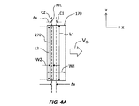
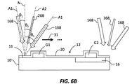
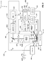
システム100の運転の例において、システムコントローラ300が第1の制御信号S1を非溶融レーザー160に送信すると、これに応答して、非溶融レーザー160は、最初の非溶融レーザービーム162を生成する。この最初の非溶融レーザービーム162は、非溶融光学システム166に受け入れられ、ここで非溶融レーザービーム168が形成される。非溶融レーザービーム168は、第1光学軸A1に沿って進み、ウエハ表面12において非溶融ラインイメージ170を形成する。
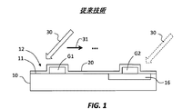
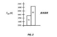
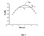
本発明にかかる超高速レーザーアニーリングシステムおよび方法の利点は、前述したパターン密度効果の不利益を軽減することによってウエハ表面12の温度均一性を向上させる点にある。第1に、レーザーアニーリング処理の実施に関係する温度変動(すなわち、非均一性)ΔTは、下記の数式によって見積もることができる。
Claims (34)
- パターン付き表面および溶融温度を有する半導体基板のアニーリング方法であって、
前記溶融温度から400℃以内にある非溶融温度Tnonmeltまで前記パターン付き表面を加熱する少なくとも一つの第1レーザービームで前記パターン付き表面を走査し、
パルス状であり、かつ、前記非溶融温度から前記溶融温度まで前記パターン付き表面を加熱する、前記第1レーザービームと関連する少なくとも一つの第2レーザービームで前記パターン付き表面を走査する方法。 - 前記第1レーザービームで走査して、前記溶融温度よりも約50℃から約400℃低い非溶融温度まで前記パターン付き表面を加熱する工程を有する、請求項1に記載の方法。
- 前記少なくとも一つの第1レーザービームは、前記パターン付き表面において少なくとも一つの非溶融ラインイメージを形成し、
前記少なくとも一つの第2レーザービームは、前記パターン付き表面において少なくとも一つの溶融ラインイメージを形成し、
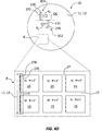
前記パターン付き表面において、前記少なくとも一つの溶融ラインイメージは、前記少なくとも一つの非溶融ラインイメージと部分的に重なり合っている、請求項1または2に記載の方法。 - 前記少なくとも一つの非溶融ラインイメージおよび前記少なくとも一つの溶融ラインイメージの一方は、前記パターン付き表面における領域の寸法に対応した長さに形成されている、請求項3に記載の方法。
- 前記少なくとも一つの第1レーザービームおよび前記少なくとも一つの第2レーザービームは、複数のICチップの間における隙間内で重なり合うように走査を行う、請求項1から4のいずれかに記載の方法。
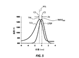
- 前記少なくとも一つの非溶融ラインイメージは、前記少なくとも一つの第1レーザービームで前記パターン付き表面を走査することによる、前記パターン付き表面の最大非溶融温度に対応するピーク温度軸に関連付けされており、
前記少なくとも一つの非溶融ラインイメージおよび前記少なくとも一つの溶融ラインイメージによる走査は、前記少なくとも一つの溶融ラインイメージが実質的に前記少なくとも一つの非溶融ラインイメージの前記ピーク温度軸に沿って形成されるようにして実行される、請求項3に記載の方法。 - 前記少なくとも一つの非溶融ラインイメージおよび前記少なくとも一つの溶融ラインイメージによる前記走査は、前記少なくとも一つの第1レーザービームによって走査される前記パターン付き表面における各点が前記少なくとも一つの第2レーザービームからの少なくとも一つの光パルスを受けるように実行される、請求項1から6のいずれかに記載の方法。
- 前記少なくとも一つの第1レーザービームは、走査中における、前記パターン付き表面上での100マイクロ秒から20ミリ秒の間の滞留時間を有している、請求項1から7のいずれかに記載の方法。
- 前記少なくとも一つの第1レーザービームはCO2レーザーを用いて生成される、請求項1から8のいずれかに記載の方法。
- 前記少なくとも一つの第1レーザービームは、実質的にブルースター角で前記パターン付き表面に入射する、請求項1から9のいずれかに記載の方法。
- 最小非溶融温度Tnonmeltが、下記の関係に基づいて決定される、請求項1から10のいずれかに記載の方法。
ここで、ΔTは基板表面温度ムラの許容量であり、ΔTmeltは従来の溶融レーザーアニーリングによるパターン密度効果に起因する基板表面温度ムラであり、Tmeltは前記基板の溶融温度であり、Tsubは当初の基板表面温度である。 - 前記少なくとも一つの第1レーザービームおよび少なくとも一つの第2レーザービームは、前記パターン付き表面付近のガス状のドーパントプレカーサを伴って走査を行う、請求項1から11のいずれかに記載の方法。
- 前記走査は、二つの第1レーザービームおよび一つの第2レーザービームを用いて実施される、請求項1から12のいずれかに記載の方法。
- 吸収層および反射防止層の内の少なくとも一方が前記パターン付き表面上に配設されている、請求項1から13のいずれかに記載の方法。
- 前記パターン付き表面はドーパントプロファイルを含んでおり、前記ドーパントプロファイルは、a)前記少なくとも一つの第1レーザービームおよびb)前記少なくとも一つの第2レーザービームの少なくとも一方を調整することによって調整される、請求項1から14のいずれかに記載の方法。
- パターン付き表面および溶融温度を有する半導体基板のレーザーアニーリングに用いられるシステムであって、
前記溶融温度から約400℃内にある非溶融温度Tnonmeltまで前記パターン付き表面を加熱する少なくとも一つの第1レーザービームを生成するとともに、前記少なくとも一つの第1レーザービームで前記パターン付き表面を走査する第1レーザーシステムと、
パルス状で、かつ、前記非溶融温度から前記溶融温度まで前記パターン付き表面を加熱する少なくとも一つの第2レーザービームを生成するとともに、前記第1レーザービームに関連して前記少なくとも一つの第2レーザービームで前記パターン付き表面を走査する第2レーザーシステムとを備えるシステム。 - 前記少なくとも一つの第1レーザービームは、前記パターン付き表面における少なくとも一つの非溶融ラインイメージを形成し、
前記第2レーザービームは、前記パターン付き表面における少なくとも一つの溶融ラインイメージを形成し、
前記第1レーザーシステムおよび前記第2レーザーシステムは、前記少なくとも一つの溶融ラインイメージおよび前記少なくとも一つの非溶融ラインイメージを前記パターン付き表面において少なくとも部分的に重複させる、請求項16に記載のシステム。 - 前記少なくとも一つの非溶融ラインイメージは、前記少なくとも一つの第1レーザービームによる前記パターン付き表面の走査に起因する前記パターン付き表面の最大非溶融に対応するピーク温度軸に関連し、かつ、
前記第1レーザーシステムおよび前記第2レーザーシステムは、前記少なくとも一つの溶融ラインイメージが、実質的に前記少なくとも一つの非溶融ラインイメージの前記ピーク温度軸に沿って形成されるように構成されている、請求項17に記載のシステム。 - 前記少なくとも一つの第1レーザービームを生成するCO2レーザーをさらに含んでいる、請求項16から18のいずれかに記載のシステム。
- 前記第1レーザーシステムは、前記少なくとも一つの第1レーザービームが前記パターン付き表面に対して実質的にブルースター角で入射するように構成されている、請求項16から19のいずれかに記載のシステム。
- ガス状のドーパントプレカーサを前記パターン付き表面付近で使用可能にするチャンバーをさらに有する、請求項16から20のいずれかに記載のシステム。
- パターン付き表面および所定の溶融温度Tmeltを有する基板のレーザーアニーリング方法であって、
前記パターン付き表面における温度ムラΔTを選択し、
下記の関係から最低非溶融温度Tnonmeltを決定し、
ここで、ΔTmeltは、従来の一つのビームによる溶融レーザーアニーリングによるパターン密度効果に起因するパターン付き表面温度ムラであり、また、Tsubは、前記パターン付き表面の当初温度である。
少なくとも一つの第1レーザービームで走査して前記パターン付き表面を前記最小非溶融温度Tnonmeltから前記溶融温度よりも約50℃低い温度の範囲の非溶融温度まで加熱し、前記第1レーザービームに関連する少なくとも一つの第2パルス状レーザービームで走査して前記基板溶融温度Tmeltまで前記パターン付き表面を加熱するレーザーアニーリングを実施する方法。 - 前記少なくとも一つの第1レーザービームはCO2レーザーである、請求項22に記載の方法。
- 前記少なくとも一つの第1レーザービームは、前記パターン付き表面に対してブルースター角あるいはそれに近い角度で向けられている、請求項22または請求項23に記載の方法。
- 前記少なくとも一つの第1レーザービームは偏光されている、請求項22から24のいずれかに記載の方法。
- 前記少なくとも一つの第2レーザービームは繰返し率が1kHz以上である、請求項22から25のいずれかに記載の方法。
- 前記少なくとも一つの第2レーザービームは、エキシマレーザー、ダイオード励起の固体レーザー、Qスイッチレーザー、および周波数変換レーザーのうちの一つを用いて生成される、請求項22から26のいずれかに記載の方法。
- 前記少なくとも一つの第2レーザービームは、20Wから500Wの出力で提供される、請求項22から27のいずれかに記載の方法。
- 前記走査は、二つの第1レーザービームと一つの第2レーザービームとで実施される、請求項22から28のいずれかに記載の方法。
- 前記少なくとも一つの第1レーザービームおよび前記少なくとも一つの第2レーザービームは、前記パターン付き表面の近傍のガス状ドーパントプレカーサを伴って走査を行う、請求項22から29のいずれかに記載の方法。
- 前記パターン付き表面において、前記少なくとも一つの第1レーザービームで少なくとも一つの非溶融ラインイメージが形成されるとともに、前記少なくとも一つの第2レーザービームで少なくとも一つの溶融ラインイメージが形成され、
前記少なくとも一つの非溶融ラインイメージおよび前記少なくとも一つの溶融ラインイメージの一方が前記パターン付き表面における領域の寸法に対応した長さを有している、請求項22から30のいずれかに記載の方法。 - 前記少なくとも一つの非溶融ラインイメージおよび前記少なくとも一つの溶融ラインイメージは、前記パターン付き表面上における複数のICチップの隙間において互いに重なるようにして走査をする、請求項31に記載の方法。
- 吸収層および反射防止層の内、少なくとも一方が前記パターン付き表面上に配設されている請求項22から32のいずれかに記載の方法。
- 前記パターン付き表面は、前記少なくとも一つの第1レーザービームおよび前記少なくとも一つの第2レーザービームの内、少なくとも一方を調整することによって調整されるドーパントプロファイルを有している、請求項22から33のいずれかに記載の方法。
Applications Claiming Priority (2)
| Application Number | Priority Date | Filing Date | Title |
|---|---|---|---|
| US13/134,408 US8309474B1 (en) | 2011-06-07 | 2011-06-07 | Ultrafast laser annealing with reduced pattern density effects in integrated circuit fabrication |
| US13/134,408 | 2011-06-07 |
Publications (2)
| Publication Number | Publication Date |
|---|---|
| JP2012256879A true JP2012256879A (ja) | 2012-12-27 |
| JP5602787B2 JP5602787B2 (ja) | 2014-10-08 |
Family
ID=47114488
Family Applications (1)
| Application Number | Title | Priority Date | Filing Date |
|---|---|---|---|
| JP2012112240A Expired - Fee Related JP5602787B2 (ja) | 2011-06-07 | 2012-05-16 | 集積回路の製造における、パターン密度効果を低減させた超高速レーザーアニーリング |
Country Status (5)
| Country | Link |
|---|---|
| US (1) | US8309474B1 (ja) |
| JP (1) | JP5602787B2 (ja) |
| KR (1) | KR20120135867A (ja) |
| SG (1) | SG186542A1 (ja) |
| TW (1) | TWI497600B (ja) |
Cited By (6)
| Publication number | Priority date | Publication date | Assignee | Title |
|---|---|---|---|---|
| JP2016105470A (ja) * | 2014-11-24 | 2016-06-09 | ウルトラテック インク | 欠陥アニーリング及びドーパント活性化のための高性能線形成光学システム及び方法 |
| KR20180098383A (ko) * | 2015-12-30 | 2018-09-03 | 상하이 마이크로 일렉트로닉스 이큅먼트(그룹) 컴퍼니 리미티드 | 레이저 어닐링 장치 및 그 어닐링 방법 |
| JP2019125762A (ja) * | 2018-01-19 | 2019-07-25 | 富士電機株式会社 | 不純物導入方法及び半導体装置の製造方法 |
| JP2019125748A (ja) * | 2018-01-18 | 2019-07-25 | トヨタ自動車株式会社 | 半導体装置の製造方法 |
| JP2019125761A (ja) * | 2018-01-19 | 2019-07-25 | 富士電機株式会社 | 不純物導入装置、不純物導入方法及び炭化ケイ素半導体装置の製造方法 |
| JP2022061475A (ja) * | 2020-09-18 | 2022-04-18 | レイザー システムズ アンド ソリューションズ オブ ヨーロッパ | 不均一性の照射を最小限に抑えるためのシステムと方法 |
Families Citing this family (16)
| Publication number | Priority date | Publication date | Assignee | Title |
|---|---|---|---|---|
| US8546805B2 (en) * | 2012-01-27 | 2013-10-01 | Ultratech, Inc. | Two-beam laser annealing with improved temperature performance |
| US9490128B2 (en) * | 2012-08-27 | 2016-11-08 | Ultratech, Inc. | Non-melt thin-wafer laser thermal annealing methods |
| US9958709B2 (en) | 2013-08-16 | 2018-05-01 | Applied Materials, Inc. | Dynamic optical valve for mitigating non-uniform heating in laser processing |
| US9559023B2 (en) | 2014-06-23 | 2017-01-31 | Ultratech, Inc. | Systems and methods for reducing beam instability in laser annealing |
| US9613828B2 (en) | 2014-06-24 | 2017-04-04 | Ultratech, Inc. | Method of laser annealing a semiconductor wafer with localized control of ambient oxygen |
| CN107578991A (zh) * | 2014-07-21 | 2018-01-12 | 应用材料公司 | 扫描脉冲退火装置及方法 |
| WO2016068741A1 (ru) * | 2014-10-28 | 2016-05-06 | Общество С Ограниченной Ответственностью "Солэкс-С" | Способ лазерного легирования и устройство для его реализации |
| US10083843B2 (en) | 2014-12-17 | 2018-09-25 | Ultratech, Inc. | Laser annealing systems and methods with ultra-short dwell times |
| US10247952B2 (en) | 2015-03-04 | 2019-04-02 | Coherent Lasersystems Gmbh & Co. Kg | Polarization-controlled laser line-projector |
| US9859121B2 (en) * | 2015-06-29 | 2018-01-02 | International Business Machines Corporation | Multiple nanosecond laser pulse anneal processes and resultant semiconductor structure |
| KR102013670B1 (ko) * | 2017-05-18 | 2019-08-26 | 세메스 주식회사 | 기판 처리 장치 및 기판 처리 방법 |
| KR101962859B1 (ko) * | 2017-05-18 | 2019-03-28 | 세메스 주식회사 | 기판 처리 장치 및 기판 처리 방법 |
| US11352698B2 (en) | 2019-04-25 | 2022-06-07 | Samsung Electronics Co., Ltd. | Atomic layer deposition apparatus and methods of fabricating semiconductor devices using the same |
| US11909091B2 (en) | 2020-05-19 | 2024-02-20 | Kymeta Corporation | Expansion compensation structure for an antenna |
| JP7434120B2 (ja) * | 2020-09-16 | 2024-02-20 | 株式会社東芝 | 光学加工装置 |
| KR102738691B1 (ko) * | 2022-12-06 | 2024-12-05 | (주)알엔알랩 | 기판 구조체에 대한 레이저 열처리 방법 및 이를 적용한 전자 소자의 제조 방법 |
Citations (10)
| Publication number | Priority date | Publication date | Assignee | Title |
|---|---|---|---|---|
| JPH0521340A (ja) * | 1991-07-10 | 1993-01-29 | Ricoh Co Ltd | 薄膜半導体装置、その製法および製造装置 |
| JPH0974067A (ja) * | 1995-09-05 | 1997-03-18 | Mitsubishi Electric Corp | ドーピング方法及びドーピング装置 |
| JP2000133613A (ja) * | 1999-11-15 | 2000-05-12 | Seiko Epson Corp | 半導体薄膜の製造方法 |
| JP2000216088A (ja) * | 1999-01-20 | 2000-08-04 | Sony Corp | 半導体薄膜形成方法及びレ―ザ照射装置 |
| JP2004006725A (ja) * | 2002-03-26 | 2004-01-08 | Semiconductor Energy Lab Co Ltd | 半導体装置、その作製方法及び設計方法 |
| JP2004515085A (ja) * | 2000-12-04 | 2004-05-20 | ボルテック インダストリーズ リミテッド | 熱処理方法およびシステム |
| JP2004266102A (ja) * | 2003-02-28 | 2004-09-24 | Semiconductor Energy Lab Co Ltd | レーザ照射装置およびレーザ照射方法、並びに半導体装置の作製方法。 |
| JP2004281771A (ja) * | 2003-03-17 | 2004-10-07 | Sharp Corp | 半導体薄膜の結晶成長方法および結晶成長装置ならびに薄膜トランジスタの製造方法 |
| JP2008047923A (ja) * | 2006-08-17 | 2008-02-28 | Toshiba Corp | 複数の光源を用いるレーザースパイクアニール |
| JP2010109363A (ja) * | 2008-10-06 | 2010-05-13 | Ultratech Inc | プレスパイクおよびポストスパイク温度制御をともなう基板の熱処理 |
Family Cites Families (43)
| Publication number | Priority date | Publication date | Assignee | Title |
|---|---|---|---|---|
| US4234356A (en) | 1979-06-01 | 1980-11-18 | Bell Telephone Laboratories, Incorporated | Dual wavelength optical annealing of materials |
| JPS56142630A (en) | 1980-04-09 | 1981-11-07 | Fujitsu Ltd | Manufacture of semiconductor device |
| JP3211377B2 (ja) | 1992-06-17 | 2001-09-25 | ソニー株式会社 | 半導体装置の製造方法 |
| KR100255689B1 (ko) | 1993-05-27 | 2000-05-01 | 윤종용 | 반도체 레이져 소자 및 그 제조방법 |
| US6066516A (en) | 1995-06-26 | 2000-05-23 | Seiko Epson Corporation | Method for forming crystalline semiconductor layers, a method for fabricating thin film transistors, and method for fabricating solar cells and active matrix liquid crystal devices |
| US6524977B1 (en) | 1995-07-25 | 2003-02-25 | Semiconductor Energy Laboratory Co., Ltd. | Method of laser annealing using linear beam having quasi-trapezoidal energy profile for increased depth of focus |
| JP3348334B2 (ja) | 1995-09-19 | 2002-11-20 | ソニー株式会社 | 薄膜半導体装置の製造方法 |
| KR0153823B1 (ko) | 1995-10-17 | 1998-12-01 | 구자홍 | 반도체 소자 제조 방법 |
| JP3301054B2 (ja) | 1996-02-13 | 2002-07-15 | 株式会社半導体エネルギー研究所 | レーザー照射装置及びレーザー照射方法 |
| JPH1174536A (ja) | 1997-01-09 | 1999-03-16 | Sanyo Electric Co Ltd | 半導体装置の製造方法 |
| US5908307A (en) | 1997-01-31 | 1999-06-01 | Ultratech Stepper, Inc. | Fabrication method for reduced-dimension FET devices |
| JPH10244392A (ja) | 1997-03-04 | 1998-09-14 | Semiconductor Energy Lab Co Ltd | レーザー照射装置 |
| TW466772B (en) | 1997-12-26 | 2001-12-01 | Seiko Epson Corp | Method for producing silicon oxide film, method for making semiconductor device, semiconductor device, display, and infrared irradiating device |
| US5930617A (en) | 1998-03-25 | 1999-07-27 | Texas Instruments-Acer Incorporated | Method of forming deep sub-micron CMOS transistors with self-aligned silicided contact and extended S/D junction |
| KR100430231B1 (ko) | 1998-10-02 | 2004-07-19 | 엘지.필립스 엘시디 주식회사 | 레이저어닐장비 |
| US6521501B1 (en) | 1999-05-11 | 2003-02-18 | Advanced Micro Devices, Inc. | Method of forming a CMOS transistor having ultra shallow source and drain regions |
| TW487959B (en) | 1999-08-13 | 2002-05-21 | Semiconductor Energy Lab | Laser apparatus, laser annealing method, and manufacturing method of a semiconductor device |
| US6514339B1 (en) | 1999-10-29 | 2003-02-04 | Lg. Philips Co., Ltd. | Laser annealing apparatus |
| JP4514861B2 (ja) | 1999-11-29 | 2010-07-28 | 株式会社半導体エネルギー研究所 | レーザ照射装置およびレーザ照射方法および半導体装置の作製方法 |
| US6366308B1 (en) | 2000-02-16 | 2002-04-02 | Ultratech Stepper, Inc. | Laser thermal processing apparatus and method |
| US6531681B1 (en) | 2000-03-27 | 2003-03-11 | Ultratech Stepper, Inc. | Apparatus having line source of radiant energy for exposing a substrate |
| US6303476B1 (en) | 2000-06-12 | 2001-10-16 | Ultratech Stepper, Inc. | Thermally induced reflectivity switch for laser thermal processing |
| US6368947B1 (en) | 2000-06-20 | 2002-04-09 | Advanced Micro Devices, Inc. | Process utilizing a cap layer optimized to reduce gate line over-melt |
| US6479821B1 (en) | 2000-09-11 | 2002-11-12 | Ultratech Stepper, Inc. | Thermally induced phase switch for laser thermal processing |
| US6365476B1 (en) | 2000-10-27 | 2002-04-02 | Ultratech Stepper, Inc. | Laser thermal process for fabricating field-effect transistors |
| US7015422B2 (en) * | 2000-12-21 | 2006-03-21 | Mattson Technology, Inc. | System and process for heating semiconductor wafers by optimizing absorption of electromagnetic energy |
| TW200304175A (en) | 2001-11-12 | 2003-09-16 | Sony Corp | Laser annealing device and thin-film transistor manufacturing method |
| US6849831B2 (en) * | 2002-03-29 | 2005-02-01 | Mattson Technology, Inc. | Pulsed processing semiconductor heating methods using combinations of heating sources |
| US6987240B2 (en) | 2002-04-18 | 2006-01-17 | Applied Materials, Inc. | Thermal flux processing by scanning |
| US7005601B2 (en) | 2002-04-18 | 2006-02-28 | Applied Materials, Inc. | Thermal flux processing by scanning |
| US6548361B1 (en) | 2002-05-15 | 2003-04-15 | Advanced Micro Devices, Inc. | SOI MOSFET and method of fabrication |
| US6747245B2 (en) | 2002-11-06 | 2004-06-08 | Ultratech Stepper, Inc. | Laser scanning apparatus and methods for thermal processing |
| US7304005B2 (en) | 2003-03-17 | 2007-12-04 | Semiconductor Energy Laboratory Co., Ltd. | Laser irradiation apparatus, laser irradiation method, and method for manufacturing a semiconductor device |
| JP4373115B2 (ja) | 2003-04-04 | 2009-11-25 | 株式会社半導体エネルギー研究所 | 半導体装置の作製方法 |
| US7098155B2 (en) | 2003-09-29 | 2006-08-29 | Ultratech, Inc. | Laser thermal annealing of lightly doped silicon substrates |
| US7772523B2 (en) | 2004-07-30 | 2010-08-10 | Semiconductor Energy Laboratory Co., Ltd | Laser irradiation apparatus and laser irradiation method |
| US7279721B2 (en) | 2005-04-13 | 2007-10-09 | Applied Materials, Inc. | Dual wavelength thermal flux laser anneal |
| US7482254B2 (en) | 2005-09-26 | 2009-01-27 | Ultratech, Inc. | Apparatus and methods for thermally processing undoped and lightly doped substrates without pre-heating |
| US7514305B1 (en) * | 2006-06-28 | 2009-04-07 | Ultratech, Inc. | Apparatus and methods for improving the intensity profile of a beam image used to process a substrate |
| US7691755B2 (en) * | 2007-05-15 | 2010-04-06 | Applied Materials, Inc. | Plasma immersion ion implantation with highly uniform chamber seasoning process for a toroidal source reactor |
| US20090034071A1 (en) | 2007-07-31 | 2009-02-05 | Dean Jennings | Method for partitioning and incoherently summing a coherent beam |
| US7709370B2 (en) * | 2007-09-20 | 2010-05-04 | International Business Machines Corporation | Spin-on antireflective coating for integration of patternable dielectric materials and interconnect structures |
| US8026519B1 (en) | 2010-10-22 | 2011-09-27 | Ultratech, Inc. | Systems and methods for forming a time-averaged line image |
-
2011
- 2011-06-07 US US13/134,408 patent/US8309474B1/en not_active Expired - Fee Related
-
2012
- 2012-05-08 SG SG2012033775A patent/SG186542A1/en unknown
- 2012-05-16 JP JP2012112240A patent/JP5602787B2/ja not_active Expired - Fee Related
- 2012-05-24 KR KR1020120055387A patent/KR20120135867A/ko not_active Ceased
- 2012-06-06 TW TW101120334A patent/TWI497600B/zh not_active IP Right Cessation
Patent Citations (10)
| Publication number | Priority date | Publication date | Assignee | Title |
|---|---|---|---|---|
| JPH0521340A (ja) * | 1991-07-10 | 1993-01-29 | Ricoh Co Ltd | 薄膜半導体装置、その製法および製造装置 |
| JPH0974067A (ja) * | 1995-09-05 | 1997-03-18 | Mitsubishi Electric Corp | ドーピング方法及びドーピング装置 |
| JP2000216088A (ja) * | 1999-01-20 | 2000-08-04 | Sony Corp | 半導体薄膜形成方法及びレ―ザ照射装置 |
| JP2000133613A (ja) * | 1999-11-15 | 2000-05-12 | Seiko Epson Corp | 半導体薄膜の製造方法 |
| JP2004515085A (ja) * | 2000-12-04 | 2004-05-20 | ボルテック インダストリーズ リミテッド | 熱処理方法およびシステム |
| JP2004006725A (ja) * | 2002-03-26 | 2004-01-08 | Semiconductor Energy Lab Co Ltd | 半導体装置、その作製方法及び設計方法 |
| JP2004266102A (ja) * | 2003-02-28 | 2004-09-24 | Semiconductor Energy Lab Co Ltd | レーザ照射装置およびレーザ照射方法、並びに半導体装置の作製方法。 |
| JP2004281771A (ja) * | 2003-03-17 | 2004-10-07 | Sharp Corp | 半導体薄膜の結晶成長方法および結晶成長装置ならびに薄膜トランジスタの製造方法 |
| JP2008047923A (ja) * | 2006-08-17 | 2008-02-28 | Toshiba Corp | 複数の光源を用いるレーザースパイクアニール |
| JP2010109363A (ja) * | 2008-10-06 | 2010-05-13 | Ultratech Inc | プレスパイクおよびポストスパイク温度制御をともなう基板の熱処理 |
Cited By (11)
| Publication number | Priority date | Publication date | Assignee | Title |
|---|---|---|---|---|
| JP2016105470A (ja) * | 2014-11-24 | 2016-06-09 | ウルトラテック インク | 欠陥アニーリング及びドーパント活性化のための高性能線形成光学システム及び方法 |
| KR20180098383A (ko) * | 2015-12-30 | 2018-09-03 | 상하이 마이크로 일렉트로닉스 이큅먼트(그룹) 컴퍼니 리미티드 | 레이저 어닐링 장치 및 그 어닐링 방법 |
| JP2019507493A (ja) * | 2015-12-30 | 2019-03-14 | シャンハイ マイクロ エレクトロニクス イクイプメント(グループ)カンパニー リミティド | レーザーアニーリング装置及びそのためのレーザーアニーリング方法 |
| KR102080613B1 (ko) | 2015-12-30 | 2020-02-24 | 상하이 마이크로 일렉트로닉스 이큅먼트(그룹) 컴퍼니 리미티드 | 레이저 어닐링 장치 및 그 어닐링 방법 |
| JP2019125748A (ja) * | 2018-01-18 | 2019-07-25 | トヨタ自動車株式会社 | 半導体装置の製造方法 |
| JP7087401B2 (ja) | 2018-01-18 | 2022-06-21 | 株式会社デンソー | 半導体装置の製造方法 |
| JP2019125762A (ja) * | 2018-01-19 | 2019-07-25 | 富士電機株式会社 | 不純物導入方法及び半導体装置の製造方法 |
| JP2019125761A (ja) * | 2018-01-19 | 2019-07-25 | 富士電機株式会社 | 不純物導入装置、不純物導入方法及び炭化ケイ素半導体装置の製造方法 |
| JP7024433B2 (ja) | 2018-01-19 | 2022-02-24 | 富士電機株式会社 | 不純物導入装置、不純物導入方法及び炭化ケイ素半導体装置の製造方法 |
| JP2022061475A (ja) * | 2020-09-18 | 2022-04-18 | レイザー システムズ アンド ソリューションズ オブ ヨーロッパ | 不均一性の照射を最小限に抑えるためのシステムと方法 |
| JP7721376B2 (ja) | 2020-09-18 | 2025-08-12 | レイザー システムズ アンド ソリューションズ オブ ヨーロッパ | 不均一性の照射を最小限に抑えるためのシステムと方法 |
Also Published As
| Publication number | Publication date |
|---|---|
| US8309474B1 (en) | 2012-11-13 |
| KR20120135867A (ko) | 2012-12-17 |
| TWI497600B (zh) | 2015-08-21 |
| JP5602787B2 (ja) | 2014-10-08 |
| SG186542A1 (en) | 2013-01-30 |
| TW201250854A (en) | 2012-12-16 |
Similar Documents
| Publication | Publication Date | Title |
|---|---|---|
| JP5602787B2 (ja) | 集積回路の製造における、パターン密度効果を低減させた超高速レーザーアニーリング | |
| US9302348B2 (en) | Ultrafast laser annealing with reduced pattern density effects in integrated circuit fabrication | |
| JP5105984B2 (ja) | ビーム照射装置、及び、レーザアニール方法 | |
| CN105719958B (zh) | 具有超短停留时间的激光退火系统及方法 | |
| JP4117020B2 (ja) | 半導体装置の製造方法および半導体装置の製造装置 | |
| JP5517396B2 (ja) | 低濃度ドープシリコン基板のレーザー熱アニール | |
| CN101459057B (zh) | 一种用于半导体制造的激光退火设备及退火工艺 | |
| TWI549191B (zh) | 管理基材退火的熱預算 | |
| JP6910742B2 (ja) | レーザアニール方法及びレーザアニール装置 | |
| US20150017817A1 (en) | Laser processing apparatus and laser processing method | |
| JP5246716B2 (ja) | 半導体基板の製造方法及びレーザアニール装置 | |
| CN115803852B (zh) | 激光退火装置的控制装置及激光退火方法 | |
| JP2012044046A (ja) | レーザアニール装置及びレーザアニール方法 | |
| EP2943973B1 (en) | Thermal processing by transmission of mid infra-red laser light through semiconductor substrate | |
| JP5660880B2 (ja) | レーザアニール方法 | |
| JP2017028017A (ja) | レーザアニール装置及びレーザアニール方法 | |
| JP2015115401A (ja) | レーザアニール方法およびレーザアニール装置 | |
| JP2014195004A (ja) | 半導体素子の製造方法及び半導体素子の製造装置 | |
| JP4307817B2 (ja) | 半導体装置の製造方法 | |
| JP2008306210A (ja) | 半導体装置の製造方法 |
Legal Events
| Date | Code | Title | Description |
|---|---|---|---|
| A621 | Written request for application examination |
Free format text: JAPANESE INTERMEDIATE CODE: A621 Effective date: 20130513 |
|
| A977 | Report on retrieval |
Free format text: JAPANESE INTERMEDIATE CODE: A971007 Effective date: 20140313 |
|
| A131 | Notification of reasons for refusal |
Free format text: JAPANESE INTERMEDIATE CODE: A131 Effective date: 20140415 |
|
| A521 | Request for written amendment filed |
Free format text: JAPANESE INTERMEDIATE CODE: A523 Effective date: 20140624 |
|
| TRDD | Decision of grant or rejection written | ||
| A01 | Written decision to grant a patent or to grant a registration (utility model) |
Free format text: JAPANESE INTERMEDIATE CODE: A01 Effective date: 20140722 |
|
| A61 | First payment of annual fees (during grant procedure) |
Free format text: JAPANESE INTERMEDIATE CODE: A61 Effective date: 20140820 |
|
| R150 | Certificate of patent or registration of utility model |
Ref document number: 5602787 Country of ref document: JP Free format text: JAPANESE INTERMEDIATE CODE: R150 |
|
| R250 | Receipt of annual fees |
Free format text: JAPANESE INTERMEDIATE CODE: R250 |
|
| R250 | Receipt of annual fees |
Free format text: JAPANESE INTERMEDIATE CODE: R250 |
|
| LAPS | Cancellation because of no payment of annual fees |