JP2012506158A - 低温基板上の薄膜を高速で反応させる方法および装置 - Google Patents
低温基板上の薄膜を高速で反応させる方法および装置 Download PDFInfo
- Publication number
- JP2012506158A JP2012506158A JP2011532314A JP2011532314A JP2012506158A JP 2012506158 A JP2012506158 A JP 2012506158A JP 2011532314 A JP2011532314 A JP 2011532314A JP 2011532314 A JP2011532314 A JP 2011532314A JP 2012506158 A JP2012506158 A JP 2012506158A
- Authority
- JP
- Japan
- Prior art keywords
- thin film
- gas atmosphere
- low temperature
- temperature substrate
- film layer
- Prior art date
- Legal status (The legal status is an assumption and is not a legal conclusion. Google has not performed a legal analysis and makes no representation as to the accuracy of the status listed.)
- Granted
Links
- 239000000758 substrate Substances 0.000 title claims abstract description 49
- 239000010409 thin film Substances 0.000 title claims abstract description 45
- 238000000034 method Methods 0.000 title claims abstract description 28
- 239000007789 gas Substances 0.000 claims abstract description 37
- 229910052751 metal Inorganic materials 0.000 claims abstract description 19
- 239000002184 metal Substances 0.000 claims abstract description 19
- 230000005670 electromagnetic radiation Effects 0.000 claims abstract description 10
- UFHFLCQGNIYNRP-UHFFFAOYSA-N Hydrogen Chemical compound [H][H] UFHFLCQGNIYNRP-UHFFFAOYSA-N 0.000 claims abstract description 7
- 239000001257 hydrogen Substances 0.000 claims abstract description 7
- 229910052739 hydrogen Inorganic materials 0.000 claims abstract description 7
- 229920000642 polymer Polymers 0.000 claims abstract description 4
- 229910052724 xenon Inorganic materials 0.000 claims description 12
- FHNFHKCVQCLJFQ-UHFFFAOYSA-N xenon atom Chemical compound [Xe] FHNFHKCVQCLJFQ-UHFFFAOYSA-N 0.000 claims description 12
- QPLDLSVMHZLSFG-UHFFFAOYSA-N Copper oxide Chemical compound [Cu]=O QPLDLSVMHZLSFG-UHFFFAOYSA-N 0.000 claims description 9
- 239000005751 Copper oxide Substances 0.000 claims description 8
- 229910000431 copper oxide Inorganic materials 0.000 claims description 8
- 229930195733 hydrocarbon Natural products 0.000 claims description 4
- 150000002430 hydrocarbons Chemical class 0.000 claims description 4
- 239000004215 Carbon black (E152) Substances 0.000 claims description 3
- 230000001360 synchronised effect Effects 0.000 claims description 3
- MUMZUERVLWJKNR-UHFFFAOYSA-N oxoplatinum Chemical compound [Pt]=O MUMZUERVLWJKNR-UHFFFAOYSA-N 0.000 claims description 2
- 229910003445 palladium oxide Inorganic materials 0.000 claims description 2
- 229910003446 platinum oxide Inorganic materials 0.000 claims description 2
- 150000002736 metal compounds Chemical class 0.000 claims 5
- JQPTYAILLJKUCY-UHFFFAOYSA-N palladium(ii) oxide Chemical compound [O-2].[Pd+2] JQPTYAILLJKUCY-UHFFFAOYSA-N 0.000 claims 1
- 229910044991 metal oxide Inorganic materials 0.000 abstract description 14
- 150000004706 metal oxides Chemical class 0.000 abstract description 14
- VNWKTOKETHGBQD-UHFFFAOYSA-N methane Chemical compound C VNWKTOKETHGBQD-UHFFFAOYSA-N 0.000 abstract description 4
- 238000001723 curing Methods 0.000 description 15
- RYGMFSIKBFXOCR-UHFFFAOYSA-N Copper Chemical compound [Cu] RYGMFSIKBFXOCR-UHFFFAOYSA-N 0.000 description 13
- 229910052802 copper Inorganic materials 0.000 description 13
- 239000010949 copper Substances 0.000 description 13
- 230000005855 radiation Effects 0.000 description 9
- 239000010408 film Substances 0.000 description 8
- 239000002245 particle Substances 0.000 description 8
- BQCADISMDOOEFD-UHFFFAOYSA-N Silver Chemical compound [Ag] BQCADISMDOOEFD-UHFFFAOYSA-N 0.000 description 5
- 229910052709 silver Inorganic materials 0.000 description 5
- 239000004332 silver Substances 0.000 description 5
- QGZKDVFQNNGYKY-UHFFFAOYSA-N Ammonia Chemical compound N QGZKDVFQNNGYKY-UHFFFAOYSA-N 0.000 description 4
- 239000004020 conductor Substances 0.000 description 4
- 238000010586 diagram Methods 0.000 description 4
- 239000004065 semiconductor Substances 0.000 description 4
- 230000015572 biosynthetic process Effects 0.000 description 3
- 238000010438 heat treatment Methods 0.000 description 3
- 239000010453 quartz Substances 0.000 description 3
- VYPSYNLAJGMNEJ-UHFFFAOYSA-N silicon dioxide Inorganic materials O=[Si]=O VYPSYNLAJGMNEJ-UHFFFAOYSA-N 0.000 description 3
- 238000005245 sintering Methods 0.000 description 3
- OKTJSMMVPCPJKN-UHFFFAOYSA-N Carbon Chemical compound [C] OKTJSMMVPCPJKN-UHFFFAOYSA-N 0.000 description 2
- ATUOYWHBWRKTHZ-UHFFFAOYSA-N Propane Chemical compound CCC ATUOYWHBWRKTHZ-UHFFFAOYSA-N 0.000 description 2
- 150000001412 amines Chemical class 0.000 description 2
- 229910021529 ammonia Inorganic materials 0.000 description 2
- 238000013459 approach Methods 0.000 description 2
- 229910052799 carbon Inorganic materials 0.000 description 2
- 150000004770 chalcogenides Chemical class 0.000 description 2
- 238000005229 chemical vapour deposition Methods 0.000 description 2
- 238000000354 decomposition reaction Methods 0.000 description 2
- 238000009792 diffusion process Methods 0.000 description 2
- 229910001922 gold oxide Inorganic materials 0.000 description 2
- 238000002844 melting Methods 0.000 description 2
- 230000008018 melting Effects 0.000 description 2
- 239000002923 metal particle Substances 0.000 description 2
- 150000002739 metals Chemical class 0.000 description 2
- 230000003287 optical effect Effects 0.000 description 2
- 230000003647 oxidation Effects 0.000 description 2
- 238000007254 oxidation reaction Methods 0.000 description 2
- BASFCYQUMIYNBI-UHFFFAOYSA-N platinum Chemical compound [Pt] BASFCYQUMIYNBI-UHFFFAOYSA-N 0.000 description 2
- 239000002243 precursor Substances 0.000 description 2
- 238000007639 printing Methods 0.000 description 2
- 230000003595 spectral effect Effects 0.000 description 2
- JBRZTFJDHDCESZ-UHFFFAOYSA-N AsGa Chemical compound [As]#[Ga] JBRZTFJDHDCESZ-UHFFFAOYSA-N 0.000 description 1
- 229910004613 CdTe Inorganic materials 0.000 description 1
- 229910001218 Gallium arsenide Inorganic materials 0.000 description 1
- 229910000673 Indium arsenide Inorganic materials 0.000 description 1
- GPXJNWSHGFTCBW-UHFFFAOYSA-N Indium phosphide Chemical compound [In]#P GPXJNWSHGFTCBW-UHFFFAOYSA-N 0.000 description 1
- KZNMRPQBBZBTSW-UHFFFAOYSA-N [Au]=O Chemical compound [Au]=O KZNMRPQBBZBTSW-UHFFFAOYSA-N 0.000 description 1
- WATWJIUSRGPENY-UHFFFAOYSA-N antimony atom Chemical compound [Sb] WATWJIUSRGPENY-UHFFFAOYSA-N 0.000 description 1
- 239000013590 bulk material Substances 0.000 description 1
- UHYPYGJEEGLRJD-UHFFFAOYSA-N cadmium(2+);selenium(2-) Chemical compound [Se-2].[Cd+2] UHYPYGJEEGLRJD-UHFFFAOYSA-N 0.000 description 1
- 238000003763 carbonization Methods 0.000 description 1
- 239000000919 ceramic Substances 0.000 description 1
- 239000003610 charcoal Substances 0.000 description 1
- 238000006243 chemical reaction Methods 0.000 description 1
- 239000011248 coating agent Substances 0.000 description 1
- 238000000576 coating method Methods 0.000 description 1
- 238000000151 deposition Methods 0.000 description 1
- 239000003989 dielectric material Substances 0.000 description 1
- 239000011521 glass Substances 0.000 description 1
- PCHJSUWPFVWCPO-UHFFFAOYSA-N gold Chemical compound [Au] PCHJSUWPFVWCPO-UHFFFAOYSA-N 0.000 description 1
- 239000010931 gold Substances 0.000 description 1
- 238000007646 gravure printing Methods 0.000 description 1
- 150000004678 hydrides Chemical class 0.000 description 1
- WPYVAWXEWQSOGY-UHFFFAOYSA-N indium antimonide Chemical compound [Sb]#[In] WPYVAWXEWQSOGY-UHFFFAOYSA-N 0.000 description 1
- RPQDHPTXJYYUPQ-UHFFFAOYSA-N indium arsenide Chemical compound [In]#[As] RPQDHPTXJYYUPQ-UHFFFAOYSA-N 0.000 description 1
- 230000006698 induction Effects 0.000 description 1
- 238000007641 inkjet printing Methods 0.000 description 1
- 238000007648 laser printing Methods 0.000 description 1
- 238000004519 manufacturing process Methods 0.000 description 1
- 150000001247 metal acetylides Chemical class 0.000 description 1
- 238000002156 mixing Methods 0.000 description 1
- 230000008450 motivation Effects 0.000 description 1
- 239000002105 nanoparticle Substances 0.000 description 1
- 150000004767 nitrides Chemical class 0.000 description 1
- 238000005121 nitriding Methods 0.000 description 1
- 239000000615 nonconductor Substances 0.000 description 1
- HBEQXAKJSGXAIQ-UHFFFAOYSA-N oxopalladium Chemical compound [Pd]=O HBEQXAKJSGXAIQ-UHFFFAOYSA-N 0.000 description 1
- 238000007649 pad printing Methods 0.000 description 1
- 238000010422 painting Methods 0.000 description 1
- 239000001294 propane Substances 0.000 description 1
- 229910052594 sapphire Inorganic materials 0.000 description 1
- 239000010980 sapphire Substances 0.000 description 1
- 238000007650 screen-printing Methods 0.000 description 1
- 150000004771 selenides Chemical class 0.000 description 1
- SBIBMFFZSBJNJF-UHFFFAOYSA-N selenium;zinc Chemical compound [Se]=[Zn] SBIBMFFZSBJNJF-UHFFFAOYSA-N 0.000 description 1
- 238000001228 spectrum Methods 0.000 description 1
- 238000004544 sputter deposition Methods 0.000 description 1
- 239000011232 storage material Substances 0.000 description 1
- 150000004763 sulfides Chemical class 0.000 description 1
- 238000003786 synthesis reaction Methods 0.000 description 1
- 150000004772 tellurides Chemical class 0.000 description 1
- 238000007740 vapor deposition Methods 0.000 description 1
Images

Classifications
-
- H—ELECTRICITY
- H05—ELECTRIC TECHNIQUES NOT OTHERWISE PROVIDED FOR
- H05K—PRINTED CIRCUITS; CASINGS OR CONSTRUCTIONAL DETAILS OF ELECTRIC APPARATUS; MANUFACTURE OF ASSEMBLAGES OF ELECTRICAL COMPONENTS
- H05K1/00—Printed circuits
- H05K1/02—Details
- H05K1/09—Use of materials for the conductive, e.g. metallic pattern
-
- H—ELECTRICITY
- H05—ELECTRIC TECHNIQUES NOT OTHERWISE PROVIDED FOR
- H05K—PRINTED CIRCUITS; CASINGS OR CONSTRUCTIONAL DETAILS OF ELECTRIC APPARATUS; MANUFACTURE OF ASSEMBLAGES OF ELECTRICAL COMPONENTS
- H05K3/00—Apparatus or processes for manufacturing printed circuits
- H05K3/10—Apparatus or processes for manufacturing printed circuits in which conductive material is applied to the insulating support in such a manner as to form the desired conductive pattern
- H05K3/105—Apparatus or processes for manufacturing printed circuits in which conductive material is applied to the insulating support in such a manner as to form the desired conductive pattern by conversion of non-conductive material on or in the support into conductive material, e.g. by using an energy beam
-
- C—CHEMISTRY; METALLURGY
- C23—COATING METALLIC MATERIAL; COATING MATERIAL WITH METALLIC MATERIAL; CHEMICAL SURFACE TREATMENT; DIFFUSION TREATMENT OF METALLIC MATERIAL; COATING BY VACUUM EVAPORATION, BY SPUTTERING, BY ION IMPLANTATION OR BY CHEMICAL VAPOUR DEPOSITION, IN GENERAL; INHIBITING CORROSION OF METALLIC MATERIAL OR INCRUSTATION IN GENERAL
- C23C—COATING METALLIC MATERIAL; COATING MATERIAL WITH METALLIC MATERIAL; SURFACE TREATMENT OF METALLIC MATERIAL BY DIFFUSION INTO THE SURFACE, BY CHEMICAL CONVERSION OR SUBSTITUTION; COATING BY VACUUM EVAPORATION, BY SPUTTERING, BY ION IMPLANTATION OR BY CHEMICAL VAPOUR DEPOSITION, IN GENERAL
- C23C18/00—Chemical coating by decomposition of either liquid compounds or solutions of the coating forming compounds, without leaving reaction products of surface material in the coating; Contact plating
- C23C18/16—Chemical coating by decomposition of either liquid compounds or solutions of the coating forming compounds, without leaving reaction products of surface material in the coating; Contact plating by reduction or substitution, e.g. electroless plating
- C23C18/1601—Process or apparatus
-
- C—CHEMISTRY; METALLURGY
- C23—COATING METALLIC MATERIAL; COATING MATERIAL WITH METALLIC MATERIAL; CHEMICAL SURFACE TREATMENT; DIFFUSION TREATMENT OF METALLIC MATERIAL; COATING BY VACUUM EVAPORATION, BY SPUTTERING, BY ION IMPLANTATION OR BY CHEMICAL VAPOUR DEPOSITION, IN GENERAL; INHIBITING CORROSION OF METALLIC MATERIAL OR INCRUSTATION IN GENERAL
- C23C—COATING METALLIC MATERIAL; COATING MATERIAL WITH METALLIC MATERIAL; SURFACE TREATMENT OF METALLIC MATERIAL BY DIFFUSION INTO THE SURFACE, BY CHEMICAL CONVERSION OR SUBSTITUTION; COATING BY VACUUM EVAPORATION, BY SPUTTERING, BY ION IMPLANTATION OR BY CHEMICAL VAPOUR DEPOSITION, IN GENERAL
- C23C18/00—Chemical coating by decomposition of either liquid compounds or solutions of the coating forming compounds, without leaving reaction products of surface material in the coating; Contact plating
- C23C18/16—Chemical coating by decomposition of either liquid compounds or solutions of the coating forming compounds, without leaving reaction products of surface material in the coating; Contact plating by reduction or substitution, e.g. electroless plating
- C23C18/1601—Process or apparatus
- C23C18/1633—Process of electroless plating
- C23C18/1655—Process features
- C23C18/1658—Process features with two steps starting with metal deposition followed by addition of reducing agent
-
- C—CHEMISTRY; METALLURGY
- C23—COATING METALLIC MATERIAL; COATING MATERIAL WITH METALLIC MATERIAL; CHEMICAL SURFACE TREATMENT; DIFFUSION TREATMENT OF METALLIC MATERIAL; COATING BY VACUUM EVAPORATION, BY SPUTTERING, BY ION IMPLANTATION OR BY CHEMICAL VAPOUR DEPOSITION, IN GENERAL; INHIBITING CORROSION OF METALLIC MATERIAL OR INCRUSTATION IN GENERAL
- C23C—COATING METALLIC MATERIAL; COATING MATERIAL WITH METALLIC MATERIAL; SURFACE TREATMENT OF METALLIC MATERIAL BY DIFFUSION INTO THE SURFACE, BY CHEMICAL CONVERSION OR SUBSTITUTION; COATING BY VACUUM EVAPORATION, BY SPUTTERING, BY ION IMPLANTATION OR BY CHEMICAL VAPOUR DEPOSITION, IN GENERAL
- C23C18/00—Chemical coating by decomposition of either liquid compounds or solutions of the coating forming compounds, without leaving reaction products of surface material in the coating; Contact plating
- C23C18/16—Chemical coating by decomposition of either liquid compounds or solutions of the coating forming compounds, without leaving reaction products of surface material in the coating; Contact plating by reduction or substitution, e.g. electroless plating
- C23C18/1601—Process or apparatus
- C23C18/1633—Process of electroless plating
- C23C18/1655—Process features
- C23C18/1664—Process features with additional means during the plating process
- C23C18/1667—Radiant energy, e.g. laser
-
- C—CHEMISTRY; METALLURGY
- C23—COATING METALLIC MATERIAL; COATING MATERIAL WITH METALLIC MATERIAL; CHEMICAL SURFACE TREATMENT; DIFFUSION TREATMENT OF METALLIC MATERIAL; COATING BY VACUUM EVAPORATION, BY SPUTTERING, BY ION IMPLANTATION OR BY CHEMICAL VAPOUR DEPOSITION, IN GENERAL; INHIBITING CORROSION OF METALLIC MATERIAL OR INCRUSTATION IN GENERAL
- C23C—COATING METALLIC MATERIAL; COATING MATERIAL WITH METALLIC MATERIAL; SURFACE TREATMENT OF METALLIC MATERIAL BY DIFFUSION INTO THE SURFACE, BY CHEMICAL CONVERSION OR SUBSTITUTION; COATING BY VACUUM EVAPORATION, BY SPUTTERING, BY ION IMPLANTATION OR BY CHEMICAL VAPOUR DEPOSITION, IN GENERAL
- C23C18/00—Chemical coating by decomposition of either liquid compounds or solutions of the coating forming compounds, without leaving reaction products of surface material in the coating; Contact plating
- C23C18/16—Chemical coating by decomposition of either liquid compounds or solutions of the coating forming compounds, without leaving reaction products of surface material in the coating; Contact plating by reduction or substitution, e.g. electroless plating
- C23C18/31—Coating with metals
-
- H—ELECTRICITY
- H05—ELECTRIC TECHNIQUES NOT OTHERWISE PROVIDED FOR
- H05K—PRINTED CIRCUITS; CASINGS OR CONSTRUCTIONAL DETAILS OF ELECTRIC APPARATUS; MANUFACTURE OF ASSEMBLAGES OF ELECTRICAL COMPONENTS
- H05K3/00—Apparatus or processes for manufacturing printed circuits
-
- H—ELECTRICITY
- H05—ELECTRIC TECHNIQUES NOT OTHERWISE PROVIDED FOR
- H05K—PRINTED CIRCUITS; CASINGS OR CONSTRUCTIONAL DETAILS OF ELECTRIC APPARATUS; MANUFACTURE OF ASSEMBLAGES OF ELECTRICAL COMPONENTS
- H05K1/00—Printed circuits
- H05K1/02—Details
- H05K1/03—Use of materials for the substrate
- H05K1/0393—Flexible materials
-
- H—ELECTRICITY
- H05—ELECTRIC TECHNIQUES NOT OTHERWISE PROVIDED FOR
- H05K—PRINTED CIRCUITS; CASINGS OR CONSTRUCTIONAL DETAILS OF ELECTRIC APPARATUS; MANUFACTURE OF ASSEMBLAGES OF ELECTRICAL COMPONENTS
- H05K2203/00—Indexing scheme relating to apparatus or processes for manufacturing printed circuits covered by H05K3/00
- H05K2203/08—Treatments involving gases
- H05K2203/087—Using a reactive gas
-
- H—ELECTRICITY
- H05—ELECTRIC TECHNIQUES NOT OTHERWISE PROVIDED FOR
- H05K—PRINTED CIRCUITS; CASINGS OR CONSTRUCTIONAL DETAILS OF ELECTRIC APPARATUS; MANUFACTURE OF ASSEMBLAGES OF ELECTRICAL COMPONENTS
- H05K2203/00—Indexing scheme relating to apparatus or processes for manufacturing printed circuits covered by H05K3/00
- H05K2203/11—Treatments characterised by their effect, e.g. heating, cooling, roughening
- H05K2203/1157—Using means for chemical reduction
-
- H—ELECTRICITY
- H05—ELECTRIC TECHNIQUES NOT OTHERWISE PROVIDED FOR
- H05K—PRINTED CIRCUITS; CASINGS OR CONSTRUCTIONAL DETAILS OF ELECTRIC APPARATUS; MANUFACTURE OF ASSEMBLAGES OF ELECTRICAL COMPONENTS
- H05K2203/00—Indexing scheme relating to apparatus or processes for manufacturing printed circuits covered by H05K3/00
- H05K2203/12—Using specific substances
- H05K2203/125—Inorganic compounds, e.g. silver salt
-
- H—ELECTRICITY
- H05—ELECTRIC TECHNIQUES NOT OTHERWISE PROVIDED FOR
- H05K—PRINTED CIRCUITS; CASINGS OR CONSTRUCTIONAL DETAILS OF ELECTRIC APPARATUS; MANUFACTURE OF ASSEMBLAGES OF ELECTRICAL COMPONENTS
- H05K2203/00—Indexing scheme relating to apparatus or processes for manufacturing printed circuits covered by H05K3/00
- H05K2203/15—Position of the PCB during processing
- H05K2203/1545—Continuous processing, i.e. involving rolls moving a band-like or solid carrier along a continuous production path
Landscapes
- Chemical & Material Sciences (AREA)
- Engineering & Computer Science (AREA)
- Chemical Kinetics & Catalysis (AREA)
- General Chemical & Material Sciences (AREA)
- Mechanical Engineering (AREA)
- Materials Engineering (AREA)
- Metallurgy (AREA)
- Organic Chemistry (AREA)
- Microelectronics & Electronic Packaging (AREA)
- Manufacturing & Machinery (AREA)
- Physics & Mathematics (AREA)
- Optics & Photonics (AREA)
- Manufacturing Of Printed Wiring (AREA)
- Chemically Coating (AREA)
- Other Surface Treatments For Metallic Materials (AREA)
- Application Of Or Painting With Fluid Materials (AREA)
- Manufacture And Refinement Of Metals (AREA)
- Conductive Materials (AREA)
- Electrodes Of Semiconductors (AREA)
- Manufacturing Of Electric Cables (AREA)
- Parts Printed On Printed Circuit Boards (AREA)
- Life Sciences & Earth Sciences (AREA)
- Pest Control & Pesticides (AREA)
- Ceramic Engineering (AREA)
- Inorganic Chemistry (AREA)
- Thermal Sciences (AREA)
Abstract
Description
本出願は、米国特許法§119(e)(1)の下、2008年10月17日に出願された仮特許出願第61/196,531号に対する優先権を主張し、この仮特許出願の内容は、本明細書において参照として援用される。
1.技術分野
本発明は、一般に硬化方法に関し、特に低温基板上の薄膜を高速で反応させる方法および装置に関する。
回路上に導電体を作製するための1つのアプローチは、金属含有インクを基板上にプリントし、次に上記金属含有インク中の粒子を焼結するために基板を加熱して導電経路を形成することである。一般に、電気伝導に適した大部分の金属は、非常に高い温度まで加熱される必要があり、往々にしてこの温度は、それらの融点の200〜300℃の範囲にある。例えば、銀は、空気中で加熱することができ、その酸化物は、導電率は比較的低いが相対的に低い温度で分解することから、導電線(conductive trace)を作製するのに良い金属である。さらに、導電線を作製するための金属の選択に関して言えば、銀が最も導電性の高い金属であるという事実は、そのコストが高いことよりしばしば重要である。

S=ウェブ速度[フィート(ft)/分]
O=重複係数
W=硬化ヘッド幅[インチ(in)]
重複係数Oは、基板が受け取るストロボパルスの平均数である。例えば、ウェブ速度200フィート/分、および重複係数5、ならびに硬化ヘッド幅2.75インチでは、ストロボパルス率は72.7Hzである。
(1)H2を用いた還元(またはH2貯蔵材料用水素化物の生成)。
Claims (20)
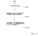
- 低温基板上の薄膜を反応させる方法であって、前記方法は、
ガス雰囲気を提供する工程;
低温基板に乗った薄膜の層を、前記ガス雰囲気中を通って移動させる工程;および
前記薄膜の層が前記ガス雰囲気中をパルス電磁放射線の線源に対して移動する間に、前記薄膜の層を前記パルス電磁放射線に曝露して、前記薄膜の層が前記ガス雰囲気と化学的に反応することを可能にする工程
を含む方法。 - 前記ガス雰囲気は水素を含む、請求項1に記載の方法。
- 前記ガス雰囲気は炭化水素ガスを含む、請求項1に記載の方法。
- 前記ガス雰囲気は1つより多いガス種を含む、請求項1に記載の方法。
- 前記薄膜は、正の還元電位を持つ金属を含んだ金属化合物である、請求項1に記載の方法。
- 前記金属化合物は酸化銅である、請求項5に記載の方法。
- 前記金属化合物は酸化白金である、請求項5に記載の方法。
- 前記金属化合物は酸化パラジウムである、請求項5に記載の方法。
- 前記薄膜は金属である、請求項1に記載の方法。
- 前記低温基板はプラスチックで作製されている、請求項1に記載の方法。
- 前記低温基板は紙で作製されている、請求項1に記載の方法。
- 前記低温基板はポリマーで作製されている、請求項1に記載の方法。
- 硬化装置であって、前記硬化装置は、
ガス雰囲気を提供するための囲い;
薄膜の層が前記ガス雰囲気と化学的に反応することを可能にすべく、低温基板に乗った前記薄膜の層にパルス電磁放射線を提供するための閃光ランプを有するストロボヘッド;および
前記薄膜の層を前記ガス雰囲気中で前記ストロボヘッドに対して移動させるためのコンベヤーシステム;および
前記閃光ランプによって発生された前記パルス電磁放射線の出力、持続時間、繰返し率および数を制御するためのストロボ制御モジュール
を備える硬化装置。 - 前記の閃光ランプはキセノン閃光ランプである、請求項13に記載の硬化装置。
- 前記低温基板は、前記パルス電磁放射線の前記繰返し率に同期化された速度で移動する、請求項13に記載の硬化装置。
- 前記低温基板は、リールツーリールシステムによって搬送される、請求項13に記載の硬化装置。
- 前記ガス雰囲気は水素を含む、請求項13の硬化装置。
- 前記ガス雰囲気は炭化水素ガスを含む、請求項13の硬化装置。
- 前記薄膜は、正の還元電位を持つ金属を含んだ金属化合物である、請求項13に記載の硬化装置。
- 前記薄膜は金属である、請求項13に記載の硬化装置。
Applications Claiming Priority (3)
| Application Number | Priority Date | Filing Date | Title |
|---|---|---|---|
| US19653108P | 2008-10-17 | 2008-10-17 | |
| US61/196,531 | 2008-10-17 | ||
| PCT/US2009/061172 WO2010045639A1 (en) | 2008-10-17 | 2009-10-19 | Method and apparatus for reacting thin films on low-temperature substrates at high speeds |
Related Child Applications (1)
| Application Number | Title | Priority Date | Filing Date |
|---|---|---|---|
| JP2013222959A Division JP2014033227A (ja) | 2008-10-17 | 2013-10-28 | 低温基板上の薄膜を高速で反応させる方法および装置 |
Publications (2)
| Publication Number | Publication Date |
|---|---|
| JP2012506158A true JP2012506158A (ja) | 2012-03-08 |
| JP5401550B2 JP5401550B2 (ja) | 2014-01-29 |
Family
ID=42106805
Family Applications (7)
| Application Number | Title | Priority Date | Filing Date |
|---|---|---|---|
| JP2011532100A Active JP5922929B2 (ja) | 2008-10-17 | 2009-03-25 | 低温基板上の薄膜を還元する方法 |
| JP2011532314A Expired - Fee Related JP5401550B2 (ja) | 2008-10-17 | 2009-10-19 | 低温基板上の薄膜を高速で反応させる方法および装置 |
| JP2013222959A Pending JP2014033227A (ja) | 2008-10-17 | 2013-10-28 | 低温基板上の薄膜を高速で反応させる方法および装置 |
| JP2014224144A Withdrawn JP2015034352A (ja) | 2008-10-17 | 2014-11-04 | 低温基板上の薄膜を還元する方法 |
| JP2016156258A Active JP6328702B2 (ja) | 2008-10-17 | 2016-08-09 | 低温基板上の薄膜を還元する方法 |
| JP2018079858A Pending JP2018131691A (ja) | 2008-10-17 | 2018-04-18 | 低温基板上の薄膜を還元する方法 |
| JP2019147583A Withdrawn JP2019189947A (ja) | 2008-10-17 | 2019-08-09 | 低温基板上の薄膜を還元する方法 |
Family Applications Before (1)
| Application Number | Title | Priority Date | Filing Date |
|---|---|---|---|
| JP2011532100A Active JP5922929B2 (ja) | 2008-10-17 | 2009-03-25 | 低温基板上の薄膜を還元する方法 |
Family Applications After (5)
| Application Number | Title | Priority Date | Filing Date |
|---|---|---|---|
| JP2013222959A Pending JP2014033227A (ja) | 2008-10-17 | 2013-10-28 | 低温基板上の薄膜を高速で反応させる方法および装置 |
| JP2014224144A Withdrawn JP2015034352A (ja) | 2008-10-17 | 2014-11-04 | 低温基板上の薄膜を還元する方法 |
| JP2016156258A Active JP6328702B2 (ja) | 2008-10-17 | 2016-08-09 | 低温基板上の薄膜を還元する方法 |
| JP2018079858A Pending JP2018131691A (ja) | 2008-10-17 | 2018-04-18 | 低温基板上の薄膜を還元する方法 |
| JP2019147583A Withdrawn JP2019189947A (ja) | 2008-10-17 | 2019-08-09 | 低温基板上の薄膜を還元する方法 |
Country Status (7)
| Country | Link |
|---|---|
| US (2) | US20110262657A1 (ja) |
| EP (2) | EP2347032B1 (ja) |
| JP (7) | JP5922929B2 (ja) |
| KR (3) | KR20150125016A (ja) |
| CN (4) | CN102245804A (ja) |
| CA (3) | CA2740618C (ja) |
| WO (2) | WO2010044904A1 (ja) |
Cited By (5)
| Publication number | Priority date | Publication date | Assignee | Title |
|---|---|---|---|---|
| JP2014011256A (ja) * | 2012-06-28 | 2014-01-20 | Dainippon Screen Mfg Co Ltd | 熱処理方法および熱処理装置 |
| JP2014067904A (ja) * | 2012-09-26 | 2014-04-17 | Dainippon Screen Mfg Co Ltd | 熱処理方法および熱処理装置 |
| JP2014534605A (ja) * | 2011-11-25 | 2014-12-18 | 昭和電工株式会社 | 導電パターン形成方法 |
| JPWO2013077448A1 (ja) * | 2011-11-24 | 2015-04-27 | 昭和電工株式会社 | 導電パターン形成方法及び光照射またはマイクロ波加熱による導電パターン形成用組成物 |
| JP2018156946A (ja) * | 2013-04-26 | 2018-10-04 | 昭和電工株式会社 | 導電パターンの製造方法及び導電パターン形成基板 |
Families Citing this family (36)
| Publication number | Priority date | Publication date | Assignee | Title |
|---|---|---|---|---|
| JP2633768B2 (ja) | 1992-05-27 | 1997-07-23 | 新日本製鐵株式会社 | 連続鋳造モールド内溶鋼流動制御方法 |
| JP2633764B2 (ja) | 1992-05-27 | 1997-07-23 | 新日本製鐵株式会社 | 連続鋳造モールド内溶鋼流動制御方法 |
| JP2633767B2 (ja) | 1992-05-27 | 1997-07-23 | 新日本製鐵株式会社 | 連続鋳造モールド内溶鋼流動制御方法 |
| JP2633769B2 (ja) | 1992-05-27 | 1997-07-23 | 新日本製鐵株式会社 | 連続鋳造モールド内溶鋼流動制御方法 |
| US8410712B2 (en) * | 2008-07-09 | 2013-04-02 | Ncc Nano, Llc | Method and apparatus for curing thin films on low-temperature substrates at high speeds |
| US8834957B2 (en) * | 2008-11-05 | 2014-09-16 | Lg Chem, Ltd. | Preparation method for an electroconductive patterned copper layer |
| US10000411B2 (en) | 2010-01-16 | 2018-06-19 | Cardinal Cg Company | Insulating glass unit transparent conductivity and low emissivity coating technology |
| US10060180B2 (en) | 2010-01-16 | 2018-08-28 | Cardinal Cg Company | Flash-treated indium tin oxide coatings, production methods, and insulating glass unit transparent conductive coating technology |
| US10000965B2 (en) | 2010-01-16 | 2018-06-19 | Cardinal Cg Company | Insulating glass unit transparent conductive coating technology |
| US8907258B2 (en) * | 2010-04-08 | 2014-12-09 | Ncc Nano, Llc | Apparatus for providing transient thermal profile processing on a moving substrate |
| US20120017829A1 (en) * | 2010-07-21 | 2012-01-26 | Xenon Corporation | Reduction of stray light during sinterinig |
| DE102011089884B4 (de) * | 2011-08-19 | 2016-03-10 | Von Ardenne Gmbh | Niedrigemittierende Beschichtung und Verfahren zur Herstellung eines niedrigemittierenden Schichtsystems |
| TWI481326B (zh) * | 2011-11-24 | 2015-04-11 | Showa Denko Kk | A conductive pattern forming method, and a conductive pattern forming composition by light irradiation or microwave heating |
| JP5991830B2 (ja) * | 2012-03-19 | 2016-09-14 | 国立大学法人大阪大学 | 導電パターン形成方法及び光照射またはマイクロ波加熱による導電パターン形成用組成物 |
| KR102122749B1 (ko) * | 2012-06-05 | 2020-06-15 | 쇼와 덴코 가부시키가이샤 | 기재막 및 소결 방법 |
| JP5283291B1 (ja) * | 2012-07-03 | 2013-09-04 | 石原薬品株式会社 | 導電膜形成方法及び焼結進行剤 |
| JP5275498B1 (ja) | 2012-07-03 | 2013-08-28 | 石原薬品株式会社 | 導電膜形成方法及び焼結進行剤 |
| WO2014026187A2 (en) * | 2012-08-10 | 2014-02-13 | Karim Rezaoul | Flash lamps in a continuous motion process |
| CN104185378A (zh) * | 2013-05-21 | 2014-12-03 | 群创光电股份有限公司 | 导电线路的制备方法、以及具有导电线路的装置 |
| FR3008228B1 (fr) | 2013-07-02 | 2015-07-17 | Commissariat Energie Atomique | Procede d'assemblage de deux composants electroniques, de type flip-chip par recuit uv, assemblage obtenu |
| KR101506504B1 (ko) * | 2013-08-22 | 2015-03-30 | (주)유니버셜스탠다드테크놀러지 | 대면적 광소결 장치 |
| DE102013113485A1 (de) * | 2013-12-04 | 2015-06-11 | Fraunhofer-Gesellschaft zur Förderung der angewandten Forschung e.V. | Verfahren zum Ausbilden einer elektrisch leitfähigen Struktur auf einem Kunststoffsubstrat |
| EP3083034A4 (en) * | 2013-12-20 | 2017-09-13 | Xenon Corporation | Continuous flash lamp sintering |
| US10015890B2 (en) | 2015-01-06 | 2018-07-03 | Fujikura Ltd. | Method of manufacturing conductive layer and wiring board |
| KR102096826B1 (ko) * | 2015-03-24 | 2020-04-03 | 쇼와 덴코 가부시키가이샤 | 도전 패턴 형성용 조성물 및 도전 패턴 형성 방법 |
| DE102016112836A1 (de) * | 2016-06-14 | 2017-12-14 | Leander Kilian Gross | Verfahren und Vorrichtung zur thermischen Behandlung eines Substrats |
| WO2019088965A1 (en) * | 2017-10-30 | 2019-05-09 | Hewlett-Packard Development Company, L.P. | Three-dimensional printing |
| KR102068285B1 (ko) * | 2018-02-12 | 2020-01-20 | 한양대학교 산학협력단 | 환원된 금속 산화물의 제조 방법 및 이를 포함하는 리튬이온 이차 전지 |
| US10959441B2 (en) | 2018-04-18 | 2021-03-30 | Xenon Corporation | Ultraviolet treatment of food products to kill microorganisms while retaining fruit bloom |
| JP7263124B2 (ja) * | 2018-05-30 | 2023-04-24 | 旭化成株式会社 | インクジェット用酸化銅インク及びこれを用いて導電性パターンを付与した導電性基板の製造方法 |
| CN110774766B (zh) * | 2018-07-31 | 2025-02-28 | 北京梦之墨科技有限公司 | 一种液态金属供墨系统的还原墨路 |
| US11028012B2 (en) | 2018-10-31 | 2021-06-08 | Cardinal Cg Company | Low solar heat gain coatings, laminated glass assemblies, and methods of producing same |
| WO2020198138A1 (en) | 2019-03-22 | 2020-10-01 | Xenon Corporation | Flash lamp system for disinfecting conveyors |
| US11996384B2 (en) | 2020-12-15 | 2024-05-28 | Pulseforge, Inc. | Method and apparatus for debonding temporarily bonded wafers in wafer-level packaging applications |
| JP7766688B2 (ja) * | 2021-05-31 | 2025-11-10 | 株式会社パイロットコーポレーション | 筆記具用インキ組成物及び筆記具用インキ組成物を収容してなる筆記具 |
| US12553129B2 (en) | 2022-12-07 | 2026-02-17 | Applied Materials, Inc. | Electrochemical reduction of surface metal oxides |
Citations (4)
| Publication number | Priority date | Publication date | Assignee | Title |
|---|---|---|---|---|
| JPH0537126A (ja) * | 1991-07-30 | 1993-02-12 | Toshiba Corp | 金属酸化物を用いた配線基板および情報記録媒体 |
| JP2004277627A (ja) * | 2003-03-18 | 2004-10-07 | Asahi Kasei Corp | インクジェット用インクおよびこれを用いた金属含有薄膜の形成方法 |
| JP2007314866A (ja) * | 2006-02-23 | 2007-12-06 | Air Products & Chemicals Inc | 導電体の作製方法 |
| JP2008522369A (ja) * | 2004-11-24 | 2008-06-26 | ノバセントリックス コーポレイション | ナノ材料組成物の電気的使用、めっき的使用および触媒的使用 |
Family Cites Families (23)
| Publication number | Priority date | Publication date | Assignee | Title |
|---|---|---|---|---|
| US3239373A (en) * | 1962-04-24 | 1966-03-08 | Louis S Hoodwin | Printed circuit process |
| FR1427315A (fr) * | 1964-02-24 | 1966-02-04 | Yawata Iron & Steel Co | Procédé pour la formation de revêtements isolants électriques sur les tôles électriques |
| US4159414A (en) * | 1978-04-25 | 1979-06-26 | Massachusetts Institute Of Technology | Method for forming electrically conductive paths |
| FR2537898A1 (fr) * | 1982-12-21 | 1984-06-22 | Univ Paris | Procede de reduction de composes metalliques par les polyols, et poudres metalliques obtenues par ce procede |
| US4592929A (en) * | 1984-02-01 | 1986-06-03 | Shipley Company Inc. | Process for metallizing plastics |
| US4526807A (en) * | 1984-04-27 | 1985-07-02 | General Electric Company | Method for deposition of elemental metals and metalloids on substrates |
| US4668533A (en) * | 1985-05-10 | 1987-05-26 | E. I. Du Pont De Nemours And Company | Ink jet printing of printed circuit boards |
| US6326130B1 (en) * | 1993-10-07 | 2001-12-04 | Mallinckrodt Baker, Inc. | Photoresist strippers containing reducing agents to reduce metal corrosion |
| EP0696515B1 (en) * | 1994-07-11 | 1998-12-02 | Agfa-Gevaert N.V. | Ink jet printing process |
| US5938848A (en) * | 1996-06-27 | 1999-08-17 | Nordson Corporation | Method and control system for applying solder flux to a printed circuit |
| KR100803186B1 (ko) * | 2000-12-15 | 2008-02-14 | 디 아리조나 보드 오브 리전츠 | 나노입자 함유 전구체를 사용한 금속의 패턴형성 방법 |
| CN1297398C (zh) * | 2001-07-06 | 2007-01-31 | 钟渊化学工业株式会社 | 层压体及其制造方法 |
| US20060159838A1 (en) * | 2005-01-14 | 2006-07-20 | Cabot Corporation | Controlling ink migration during the formation of printable electronic features |
| US20040185388A1 (en) * | 2003-01-29 | 2004-09-23 | Hiroyuki Hirai | Printed circuit board, method for producing same, and ink therefor |
| JP4416080B2 (ja) * | 2003-01-29 | 2010-02-17 | 富士フイルム株式会社 | プリント配線基板形成用インク、プリント配線基板の形成方法及びプリント配線基板 |
| JP2004277868A (ja) * | 2003-03-19 | 2004-10-07 | Mitsubishi Paper Mills Ltd | 導電性組成物の作製方法 |
| US20040234916A1 (en) * | 2003-05-21 | 2004-11-25 | Alexza Molecular Delivery Corporation | Optically ignited or electrically ignited self-contained heating unit and drug-supply unit employing same |
| JP2005071805A (ja) * | 2003-08-25 | 2005-03-17 | Fuji Photo Film Co Ltd | 金属酸化物及び/又は金属水酸化物の粒子と金属の粒子を含む組成物、組成物を用いたプリント配線基板、その製造方法及びそれに用いるインク |
| US7547647B2 (en) * | 2004-07-06 | 2009-06-16 | Hewlett-Packard Development Company, L.P. | Method of making a structure |
| JP2008527169A (ja) * | 2005-01-10 | 2008-07-24 | イシウム リサーチ デベロップメント カンパニー オブ ザ ヘブリュー ユニバーシティー オブ イエルサレム | 金属ナノ粒子の水系分散物 |
| US20060258136A1 (en) * | 2005-05-11 | 2006-11-16 | Guangjin Li | Method of forming a metal trace |
| EP2066497B1 (en) * | 2006-08-07 | 2018-11-07 | Inktec Co., Ltd. | Manufacturing methods for metal clad laminates |
| US10231344B2 (en) * | 2007-05-18 | 2019-03-12 | Applied Nanotech Holdings, Inc. | Metallic ink |
-
2009
- 2009-03-25 CA CA2740618A patent/CA2740618C/en active Active
- 2009-03-25 WO PCT/US2009/038289 patent/WO2010044904A1/en not_active Ceased
- 2009-03-25 CN CN2009801503274A patent/CN102245804A/zh active Pending
- 2009-03-25 US US13/124,781 patent/US20110262657A1/en not_active Abandoned
- 2009-03-25 EP EP09820923.2A patent/EP2347032B1/en active Active
- 2009-03-25 KR KR1020157030385A patent/KR20150125016A/ko not_active Ceased
- 2009-03-25 CN CN201510329127.2A patent/CN104894538A/zh active Pending
- 2009-03-25 JP JP2011532100A patent/JP5922929B2/ja active Active
- 2009-03-25 CA CA2910493A patent/CA2910493C/en active Active
- 2009-03-25 KR KR1020117011229A patent/KR101600559B1/ko active Active
- 2009-10-19 WO PCT/US2009/061172 patent/WO2010045639A1/en not_active Ceased
- 2009-10-19 CA CA2740786A patent/CA2740786C/en active Active
- 2009-10-19 EP EP09821387.9A patent/EP2347638B1/en active Active
- 2009-10-19 KR KR1020117011230A patent/KR101604437B1/ko active Active
- 2009-10-19 US US12/581,606 patent/US20100098874A1/en not_active Abandoned
- 2009-10-19 JP JP2011532314A patent/JP5401550B2/ja not_active Expired - Fee Related
- 2009-10-19 CN CN2009801453843A patent/CN102217429B/zh not_active Expired - Fee Related
- 2009-10-19 CN CN201310495062.XA patent/CN103796425B/zh not_active Expired - Fee Related
-
2013
- 2013-10-28 JP JP2013222959A patent/JP2014033227A/ja active Pending
-
2014
- 2014-11-04 JP JP2014224144A patent/JP2015034352A/ja not_active Withdrawn
-
2016
- 2016-08-09 JP JP2016156258A patent/JP6328702B2/ja active Active
-
2018
- 2018-04-18 JP JP2018079858A patent/JP2018131691A/ja active Pending
-
2019
- 2019-08-09 JP JP2019147583A patent/JP2019189947A/ja not_active Withdrawn
Patent Citations (4)
| Publication number | Priority date | Publication date | Assignee | Title |
|---|---|---|---|---|
| JPH0537126A (ja) * | 1991-07-30 | 1993-02-12 | Toshiba Corp | 金属酸化物を用いた配線基板および情報記録媒体 |
| JP2004277627A (ja) * | 2003-03-18 | 2004-10-07 | Asahi Kasei Corp | インクジェット用インクおよびこれを用いた金属含有薄膜の形成方法 |
| JP2008522369A (ja) * | 2004-11-24 | 2008-06-26 | ノバセントリックス コーポレイション | ナノ材料組成物の電気的使用、めっき的使用および触媒的使用 |
| JP2007314866A (ja) * | 2006-02-23 | 2007-12-06 | Air Products & Chemicals Inc | 導電体の作製方法 |
Cited By (5)
| Publication number | Priority date | Publication date | Assignee | Title |
|---|---|---|---|---|
| JPWO2013077448A1 (ja) * | 2011-11-24 | 2015-04-27 | 昭和電工株式会社 | 導電パターン形成方法及び光照射またはマイクロ波加熱による導電パターン形成用組成物 |
| JP2014534605A (ja) * | 2011-11-25 | 2014-12-18 | 昭和電工株式会社 | 導電パターン形成方法 |
| JP2014011256A (ja) * | 2012-06-28 | 2014-01-20 | Dainippon Screen Mfg Co Ltd | 熱処理方法および熱処理装置 |
| JP2014067904A (ja) * | 2012-09-26 | 2014-04-17 | Dainippon Screen Mfg Co Ltd | 熱処理方法および熱処理装置 |
| JP2018156946A (ja) * | 2013-04-26 | 2018-10-04 | 昭和電工株式会社 | 導電パターンの製造方法及び導電パターン形成基板 |
Also Published As
Similar Documents
| Publication | Publication Date | Title |
|---|---|---|
| JP5401550B2 (ja) | 低温基板上の薄膜を高速で反応させる方法および装置 | |
| US9643208B2 (en) | Method and apparatus for curing thin films on low-temperature substrates at high speeds | |
| KR101444388B1 (ko) | 저온 플라즈마 소결 장치 및 방법 | |
| Zhang et al. | Decomposition mechanisms of thin palladium acetate film with excimer UV radiation | |
| HK1162093B (en) | Method and apparatus for reacting thin films on low-temperature substrates at high speeds | |
| Manzi et al. | Plasma Jet Printing for Flexible Hybrid Electronics–A Review | |
| KR20160079202A (ko) | 산화 방지부를 구비하는 기판 열처리 시스템 |
Legal Events
| Date | Code | Title | Description |
|---|---|---|---|
| A621 | Written request for application examination |
Free format text: JAPANESE INTERMEDIATE CODE: A621 Effective date: 20120725 |
|
| A977 | Report on retrieval |
Free format text: JAPANESE INTERMEDIATE CODE: A971007 Effective date: 20130606 |
|
| A131 | Notification of reasons for refusal |
Free format text: JAPANESE INTERMEDIATE CODE: A131 Effective date: 20130611 |
|
| A521 | Request for written amendment filed |
Free format text: JAPANESE INTERMEDIATE CODE: A523 Effective date: 20130802 |
|
| TRDD | Decision of grant or rejection written | ||
| A01 | Written decision to grant a patent or to grant a registration (utility model) |
Free format text: JAPANESE INTERMEDIATE CODE: A01 Effective date: 20131002 |
|
| A61 | First payment of annual fees (during grant procedure) |
Free format text: JAPANESE INTERMEDIATE CODE: A61 Effective date: 20131028 |
|
| R150 | Certificate of patent or registration of utility model |
Ref document number: 5401550 Country of ref document: JP Free format text: JAPANESE INTERMEDIATE CODE: R150 Free format text: JAPANESE INTERMEDIATE CODE: R150 |
|
| R250 | Receipt of annual fees |
Free format text: JAPANESE INTERMEDIATE CODE: R250 |
|
| R250 | Receipt of annual fees |
Free format text: JAPANESE INTERMEDIATE CODE: R250 |
|
| R250 | Receipt of annual fees |
Free format text: JAPANESE INTERMEDIATE CODE: R250 |
|
| R250 | Receipt of annual fees |
Free format text: JAPANESE INTERMEDIATE CODE: R250 |
|
| R250 | Receipt of annual fees |
Free format text: JAPANESE INTERMEDIATE CODE: R250 |
|
| R250 | Receipt of annual fees |
Free format text: JAPANESE INTERMEDIATE CODE: R250 |
|
| R250 | Receipt of annual fees |
Free format text: JAPANESE INTERMEDIATE CODE: R250 |
|
| LAPS | Cancellation because of no payment of annual fees |