JP2013152425A - Antireflection film and optical element - Google Patents
Antireflection film and optical element Download PDFInfo
- Publication number
- JP2013152425A JP2013152425A JP2012225716A JP2012225716A JP2013152425A JP 2013152425 A JP2013152425 A JP 2013152425A JP 2012225716 A JP2012225716 A JP 2012225716A JP 2012225716 A JP2012225716 A JP 2012225716A JP 2013152425 A JP2013152425 A JP 2013152425A
- Authority
- JP
- Japan
- Prior art keywords
- layer
- refractive index
- antireflection film
- film
- intermediate layer
- Prior art date
- Legal status (The legal status is an assumption and is not a legal conclusion. Google has not performed a legal analysis and makes no representation as to the accuracy of the status listed.)
- Pending
Links
- 230000003287 optical effect Effects 0.000 title claims abstract description 67
- VYPSYNLAJGMNEJ-UHFFFAOYSA-N Silicium dioxide Chemical compound O=[Si]=O VYPSYNLAJGMNEJ-UHFFFAOYSA-N 0.000 claims abstract description 118
- 239000000463 material Substances 0.000 claims abstract description 87
- 238000000034 method Methods 0.000 claims abstract description 73
- 239000000758 substrate Substances 0.000 claims abstract description 45
- 239000011230 binding agent Substances 0.000 claims abstract description 40
- 238000000576 coating method Methods 0.000 claims abstract description 34
- 239000011248 coating agent Substances 0.000 claims abstract description 31
- 239000007788 liquid Substances 0.000 claims abstract description 21
- 239000010410 layer Substances 0.000 claims description 435
- 150000007529 inorganic bases Chemical class 0.000 claims description 27
- 230000015572 biosynthetic process Effects 0.000 claims description 24
- 150000002902 organometallic compounds Chemical class 0.000 claims description 21
- 239000013545 self-assembled monolayer Substances 0.000 claims description 16
- 229910010272 inorganic material Inorganic materials 0.000 claims description 14
- 239000011147 inorganic material Substances 0.000 claims description 14
- 239000002346 layers by function Substances 0.000 claims description 13
- 239000002094 self assembled monolayer Substances 0.000 claims description 13
- 150000003961 organosilicon compounds Chemical group 0.000 claims description 11
- 239000002245 particle Substances 0.000 claims description 11
- 238000004381 surface treatment Methods 0.000 claims description 7
- 239000002356 single layer Substances 0.000 claims description 6
- 150000003609 titanium compounds Chemical class 0.000 claims description 5
- 150000003755 zirconium compounds Chemical class 0.000 claims description 4
- 230000000694 effects Effects 0.000 abstract description 6
- 150000002736 metal compounds Chemical class 0.000 abstract description 5
- 239000010408 film Substances 0.000 description 313
- FFUAGWLWBBFQJT-UHFFFAOYSA-N hexamethyldisilazane Chemical compound C[Si](C)(C)N[Si](C)(C)C FFUAGWLWBBFQJT-UHFFFAOYSA-N 0.000 description 38
- 239000000377 silicon dioxide Substances 0.000 description 28
- 239000000470 constituent Substances 0.000 description 25
- 239000007789 gas Substances 0.000 description 22
- 230000000052 comparative effect Effects 0.000 description 19
- 239000010409 thin film Substances 0.000 description 15
- 230000003667 anti-reflective effect Effects 0.000 description 14
- UQEAIHBTYFGYIE-UHFFFAOYSA-N hexamethyldisiloxane Chemical compound C[Si](C)(C)O[Si](C)(C)C UQEAIHBTYFGYIE-UHFFFAOYSA-N 0.000 description 14
- 229910052751 metal Inorganic materials 0.000 description 14
- XKRFYHLGVUSROY-UHFFFAOYSA-N Argon Chemical compound [Ar] XKRFYHLGVUSROY-UHFFFAOYSA-N 0.000 description 12
- MYMOFIZGZYHOMD-UHFFFAOYSA-N Dioxygen Chemical compound O=O MYMOFIZGZYHOMD-UHFFFAOYSA-N 0.000 description 11
- 238000005229 chemical vapour deposition Methods 0.000 description 11
- 150000001875 compounds Chemical class 0.000 description 11
- 238000013461 design Methods 0.000 description 11
- 229910001882 dioxygen Inorganic materials 0.000 description 11
- 239000002994 raw material Substances 0.000 description 11
- 229910052814 silicon oxide Inorganic materials 0.000 description 10
- 229910010413 TiO 2 Inorganic materials 0.000 description 9
- 238000011156 evaluation Methods 0.000 description 9
- 239000002184 metal Substances 0.000 description 9
- 239000002904 solvent Substances 0.000 description 8
- OGIDPMRJRNCKJF-UHFFFAOYSA-N titanium oxide Inorganic materials [Ti]=O OGIDPMRJRNCKJF-UHFFFAOYSA-N 0.000 description 8
- VXUYXOFXAQZZMF-UHFFFAOYSA-N titanium(IV) isopropoxide Chemical compound CC(C)O[Ti](OC(C)C)(OC(C)C)OC(C)C VXUYXOFXAQZZMF-UHFFFAOYSA-N 0.000 description 8
- GWEVSGVZZGPLCZ-UHFFFAOYSA-N Titan oxide Chemical compound O=[Ti]=O GWEVSGVZZGPLCZ-UHFFFAOYSA-N 0.000 description 7
- 230000008859 change Effects 0.000 description 7
- 239000003795 chemical substances by application Substances 0.000 description 7
- 239000011347 resin Substances 0.000 description 7
- 229920005989 resin Polymers 0.000 description 7
- CZDYPVPMEAXLPK-UHFFFAOYSA-N tetramethylsilane Chemical compound C[Si](C)(C)C CZDYPVPMEAXLPK-UHFFFAOYSA-N 0.000 description 7
- 229910018072 Al 2 O 3 Inorganic materials 0.000 description 6
- KFZMGEQAYNKOFK-UHFFFAOYSA-N Isopropanol Chemical compound CC(C)O KFZMGEQAYNKOFK-UHFFFAOYSA-N 0.000 description 6
- 229910052786 argon Inorganic materials 0.000 description 6
- 239000012788 optical film Substances 0.000 description 6
- 238000006116 polymerization reaction Methods 0.000 description 6
- 235000012239 silicon dioxide Nutrition 0.000 description 6
- 238000012360 testing method Methods 0.000 description 6
- 239000010936 titanium Substances 0.000 description 6
- 229910004298 SiO 2 Inorganic materials 0.000 description 5
- 239000010419 fine particle Substances 0.000 description 5
- 238000010438 heat treatment Methods 0.000 description 5
- 125000000962 organic group Chemical group 0.000 description 5
- 238000005268 plasma chemical vapour deposition Methods 0.000 description 5
- LIVNPJMFVYWSIS-UHFFFAOYSA-N silicon monoxide Chemical compound [Si-]#[O+] LIVNPJMFVYWSIS-UHFFFAOYSA-N 0.000 description 5
- 238000007740 vapor deposition Methods 0.000 description 5
- 239000011800 void material Substances 0.000 description 5
- 239000004925 Acrylic resin Substances 0.000 description 4
- 229920000178 Acrylic resin Polymers 0.000 description 4
- 229910021193 La 2 O 3 Inorganic materials 0.000 description 4
- 230000009471 action Effects 0.000 description 4
- 229910052799 carbon Inorganic materials 0.000 description 4
- 238000004140 cleaning Methods 0.000 description 4
- 230000007547 defect Effects 0.000 description 4
- 238000010586 diagram Methods 0.000 description 4
- 238000003618 dip coating Methods 0.000 description 4
- 239000000499 gel Substances 0.000 description 4
- 125000002887 hydroxy group Chemical group [H]O* 0.000 description 4
- 239000000203 mixture Substances 0.000 description 4
- 230000003595 spectral effect Effects 0.000 description 4
- 229910006404 SnO 2 Inorganic materials 0.000 description 3
- 238000000151 deposition Methods 0.000 description 3
- -1 for example Inorganic materials 0.000 description 3
- 230000007062 hydrolysis Effects 0.000 description 3
- 238000006460 hydrolysis reaction Methods 0.000 description 3
- 239000011159 matrix material Substances 0.000 description 3
- 239000005304 optical glass Substances 0.000 description 3
- 238000009832 plasma treatment Methods 0.000 description 3
- 238000004528 spin coating Methods 0.000 description 3
- 229910052719 titanium Inorganic materials 0.000 description 3
- OKTJSMMVPCPJKN-UHFFFAOYSA-N Carbon Chemical compound [C] OKTJSMMVPCPJKN-UHFFFAOYSA-N 0.000 description 2
- 241000511976 Hoya Species 0.000 description 2
- BOTDANWDWHJENH-UHFFFAOYSA-N Tetraethyl orthosilicate Chemical compound CCO[Si](OCC)(OCC)OCC BOTDANWDWHJENH-UHFFFAOYSA-N 0.000 description 2
- RTAQQCXQSZGOHL-UHFFFAOYSA-N Titanium Chemical compound [Ti] RTAQQCXQSZGOHL-UHFFFAOYSA-N 0.000 description 2
- MCMNRKCIXSYSNV-UHFFFAOYSA-N Zirconium dioxide Chemical compound O=[Zr]=O MCMNRKCIXSYSNV-UHFFFAOYSA-N 0.000 description 2
- 150000004703 alkoxides Chemical class 0.000 description 2
- 125000000217 alkyl group Chemical group 0.000 description 2
- 150000001343 alkyl silanes Chemical class 0.000 description 2
- 238000000149 argon plasma sintering Methods 0.000 description 2
- 238000000231 atomic layer deposition Methods 0.000 description 2
- QVGXLLKOCUKJST-UHFFFAOYSA-N atomic oxygen Chemical compound [O] QVGXLLKOCUKJST-UHFFFAOYSA-N 0.000 description 2
- 238000004132 cross linking Methods 0.000 description 2
- FFUUQWKRQSBSGU-UHFFFAOYSA-N dipropylsilicon Chemical compound CCC[Si]CCC FFUUQWKRQSBSGU-UHFFFAOYSA-N 0.000 description 2
- 239000003822 epoxy resin Substances 0.000 description 2
- 239000011521 glass Substances 0.000 description 2
- 230000006872 improvement Effects 0.000 description 2
- 238000004519 manufacturing process Methods 0.000 description 2
- 238000005259 measurement Methods 0.000 description 2
- 239000012528 membrane Substances 0.000 description 2
- 108010049640 osmotic shock released antigen Proteins 0.000 description 2
- 239000001301 oxygen Substances 0.000 description 2
- 229910052760 oxygen Inorganic materials 0.000 description 2
- 238000005240 physical vapour deposition Methods 0.000 description 2
- 230000010287 polarization Effects 0.000 description 2
- 229920003229 poly(methyl methacrylate) Polymers 0.000 description 2
- 229920000647 polyepoxide Polymers 0.000 description 2
- 239000004926 polymethyl methacrylate Substances 0.000 description 2
- 238000007650 screen-printing Methods 0.000 description 2
- 238000000926 separation method Methods 0.000 description 2
- 239000007921 spray Substances 0.000 description 2
- 238000004544 sputter deposition Methods 0.000 description 2
- 238000003786 synthesis reaction Methods 0.000 description 2
- 239000012780 transparent material Substances 0.000 description 2
- 238000001771 vacuum deposition Methods 0.000 description 2
- XLYOFNOQVPJJNP-UHFFFAOYSA-N water Substances O XLYOFNOQVPJJNP-UHFFFAOYSA-N 0.000 description 2
- WYTZZXDRDKSJID-UHFFFAOYSA-N (3-aminopropyl)triethoxysilane Chemical compound CCO[Si](OCC)(OCC)CCCN WYTZZXDRDKSJID-UHFFFAOYSA-N 0.000 description 1
- HNJCRKROKIPREU-UHFFFAOYSA-N 1,1,2,2,3,3,4,4,5,5,6,6,7,7,10,10,10-heptadecafluorodecyl-dimethoxy-methylsilane Chemical compound CO[Si](C)(OC)C(F)(F)C(F)(F)C(F)(F)C(F)(F)C(F)(F)C(F)(F)C(F)(F)CCC(F)(F)F HNJCRKROKIPREU-UHFFFAOYSA-N 0.000 description 1
- 125000003903 2-propenyl group Chemical group [H]C([*])([H])C([H])=C([H])[H] 0.000 description 1
- ZYAASQNKCWTPKI-UHFFFAOYSA-N 3-[dimethoxy(methyl)silyl]propan-1-amine Chemical compound CO[Si](C)(OC)CCCN ZYAASQNKCWTPKI-UHFFFAOYSA-N 0.000 description 1
- OXYZDRAJMHGSMW-UHFFFAOYSA-N 3-chloropropyl(trimethoxy)silane Chemical compound CO[Si](OC)(OC)CCCCl OXYZDRAJMHGSMW-UHFFFAOYSA-N 0.000 description 1
- KEZMLECYELSZDC-UHFFFAOYSA-N 3-chloropropyl-diethoxy-methylsilane Chemical compound CCO[Si](C)(OCC)CCCCl KEZMLECYELSZDC-UHFFFAOYSA-N 0.000 description 1
- KNTKCYKJRSMRMZ-UHFFFAOYSA-N 3-chloropropyl-dimethoxy-methylsilane Chemical compound CO[Si](C)(OC)CCCCl KNTKCYKJRSMRMZ-UHFFFAOYSA-N 0.000 description 1
- BZCWFJMZVXHYQA-UHFFFAOYSA-N 3-dimethoxysilylpropyl 2-methylprop-2-enoate Chemical compound CO[SiH](OC)CCCOC(=O)C(C)=C BZCWFJMZVXHYQA-UHFFFAOYSA-N 0.000 description 1
- URDOJQUSEUXVRP-UHFFFAOYSA-N 3-triethoxysilylpropyl 2-methylprop-2-enoate Chemical compound CCO[Si](OCC)(OCC)CCCOC(=O)C(C)=C URDOJQUSEUXVRP-UHFFFAOYSA-N 0.000 description 1
- XDLMVUHYZWKMMD-UHFFFAOYSA-N 3-trimethoxysilylpropyl 2-methylprop-2-enoate Chemical compound CO[Si](OC)(OC)CCCOC(=O)C(C)=C XDLMVUHYZWKMMD-UHFFFAOYSA-N 0.000 description 1
- NLTGMIOSTSUEES-UHFFFAOYSA-N CCCCO[SiH](C(C)CC)OCCCC Chemical compound CCCCO[SiH](C(C)CC)OCCCC NLTGMIOSTSUEES-UHFFFAOYSA-N 0.000 description 1
- IPKWLNHXHVMOBJ-UHFFFAOYSA-N CCCCO[SiH](CCC)CCC Chemical compound CCCCO[SiH](CCC)CCC IPKWLNHXHVMOBJ-UHFFFAOYSA-N 0.000 description 1
- NTHKCSDJQGWPJY-UHFFFAOYSA-N CCCC[SiH](OC)OC Chemical compound CCCC[SiH](OC)OC NTHKCSDJQGWPJY-UHFFFAOYSA-N 0.000 description 1
- PMPGBDYFVDJHLK-UHFFFAOYSA-N CCCC[SiH](OCCC)OCCC Chemical compound CCCC[SiH](OCCC)OCCC PMPGBDYFVDJHLK-UHFFFAOYSA-N 0.000 description 1
- KWFZAAGYIJTNNS-UHFFFAOYSA-N CCCO[Si](C)OCCC Chemical compound CCCO[Si](C)OCCC KWFZAAGYIJTNNS-UHFFFAOYSA-N 0.000 description 1
- NOIFXTRHAJAXOW-UHFFFAOYSA-N CCO[SiH](OCC)C(C)CC Chemical compound CCO[SiH](OCC)C(C)CC NOIFXTRHAJAXOW-UHFFFAOYSA-N 0.000 description 1
- 229910052684 Cerium Inorganic materials 0.000 description 1
- KRHYYFGTRYWZRS-UHFFFAOYSA-M Fluoride anion Chemical compound [F-] KRHYYFGTRYWZRS-UHFFFAOYSA-M 0.000 description 1
- YCKRFDGAMUMZLT-UHFFFAOYSA-N Fluorine atom Chemical compound [F] YCKRFDGAMUMZLT-UHFFFAOYSA-N 0.000 description 1
- UFHFLCQGNIYNRP-UHFFFAOYSA-N Hydrogen Chemical compound [H][H] UFHFLCQGNIYNRP-UHFFFAOYSA-N 0.000 description 1
- 229910003849 O-Si Inorganic materials 0.000 description 1
- 229910003872 O—Si Inorganic materials 0.000 description 1
- 229910052777 Praseodymium Inorganic materials 0.000 description 1
- BLRPTPMANUNPDV-UHFFFAOYSA-N Silane Chemical compound [SiH4] BLRPTPMANUNPDV-UHFFFAOYSA-N 0.000 description 1
- 239000004965 Silica aerogel Substances 0.000 description 1
- 238000010521 absorption reaction Methods 0.000 description 1
- 125000003342 alkenyl group Chemical group 0.000 description 1
- 125000003545 alkoxy group Chemical group 0.000 description 1
- JYMITAMFTJDTAE-UHFFFAOYSA-N aluminum zinc oxygen(2-) Chemical compound [O-2].[Al+3].[Zn+2] JYMITAMFTJDTAE-UHFFFAOYSA-N 0.000 description 1
- 125000003368 amide group Chemical group 0.000 description 1
- 230000003373 anti-fouling effect Effects 0.000 description 1
- 125000003710 aryl alkyl group Chemical group 0.000 description 1
- 239000012298 atmosphere Substances 0.000 description 1
- 238000007611 bar coating method Methods 0.000 description 1
- 239000010953 base metal Substances 0.000 description 1
- 125000001797 benzyl group Chemical group [H]C1=C([H])C([H])=C(C([H])=C1[H])C([H])([H])* 0.000 description 1
- GVCJFBPGIITONJ-UHFFFAOYSA-N butan-2-yl(dimethoxy)silane Chemical compound CCC(C)[SiH](OC)OC GVCJFBPGIITONJ-UHFFFAOYSA-N 0.000 description 1
- VXGZTBCZUKFZLV-UHFFFAOYSA-N butan-2-yl(dipropoxy)silane Chemical compound CCCO[SiH](C(C)CC)OCCC VXGZTBCZUKFZLV-UHFFFAOYSA-N 0.000 description 1
- 125000004369 butenyl group Chemical group C(=CCC)* 0.000 description 1
- 125000004106 butoxy group Chemical group [*]OC([H])([H])C([H])([H])C(C([H])([H])[H])([H])[H] 0.000 description 1
- CWLHIHREMPKWDY-UHFFFAOYSA-N butoxy(diethyl)silane Chemical compound CCCCO[SiH](CC)CC CWLHIHREMPKWDY-UHFFFAOYSA-N 0.000 description 1
- SOKKGFZWZZLHEK-UHFFFAOYSA-N butoxy(dimethyl)silane Chemical compound CCCCO[SiH](C)C SOKKGFZWZZLHEK-UHFFFAOYSA-N 0.000 description 1
- DALMMFLTKSAASI-UHFFFAOYSA-N butoxy-ethyl-methylsilane Chemical compound CCCCO[SiH](C)CC DALMMFLTKSAASI-UHFFFAOYSA-N 0.000 description 1
- ZZHNUBIHHLQNHX-UHFFFAOYSA-N butoxysilane Chemical compound CCCCO[SiH3] ZZHNUBIHHLQNHX-UHFFFAOYSA-N 0.000 description 1
- 125000000484 butyl group Chemical group [H]C([*])([H])C([H])([H])C([H])([H])C([H])([H])[H] 0.000 description 1
- ZEZXMFBCRYGNNP-UHFFFAOYSA-N butyl(diethoxy)silane Chemical compound CCCC[SiH](OCC)OCC ZEZXMFBCRYGNNP-UHFFFAOYSA-N 0.000 description 1
- 125000002915 carbonyl group Chemical group [*:2]C([*:1])=O 0.000 description 1
- 238000006243 chemical reaction Methods 0.000 description 1
- 239000003431 cross linking reagent Substances 0.000 description 1
- 150000001925 cycloalkenes Chemical class 0.000 description 1
- 125000000113 cyclohexyl group Chemical group [H]C1([H])C([H])([H])C([H])([H])C([H])(*)C([H])([H])C1([H])[H] 0.000 description 1
- SJJCABYOVIHNPZ-UHFFFAOYSA-N cyclohexyl-dimethoxy-methylsilane Chemical compound CO[Si](C)(OC)C1CCCCC1 SJJCABYOVIHNPZ-UHFFFAOYSA-N 0.000 description 1
- 230000006837 decompression Effects 0.000 description 1
- 230000003247 decreasing effect Effects 0.000 description 1
- 238000011161 development Methods 0.000 description 1
- DOJBUDQOPFLZAZ-UHFFFAOYSA-N dibutoxy(butyl)silane Chemical compound CCCCO[SiH](CCCC)OCCCC DOJBUDQOPFLZAZ-UHFFFAOYSA-N 0.000 description 1
- PLTKQPNYFHYCNQ-UHFFFAOYSA-N dibutoxy(ethyl)silane Chemical compound CCCCO[SiH](CC)OCCCC PLTKQPNYFHYCNQ-UHFFFAOYSA-N 0.000 description 1
- TTYHSEJYYROOSI-UHFFFAOYSA-N dibutoxy(methyl)silane Chemical compound CCCCO[SiH](C)OCCCC TTYHSEJYYROOSI-UHFFFAOYSA-N 0.000 description 1
- MSXQSMNVGLDLOK-UHFFFAOYSA-N dibutoxy(phenyl)silane Chemical compound CCCCO[SiH](OCCCC)C1=CC=CC=C1 MSXQSMNVGLDLOK-UHFFFAOYSA-N 0.000 description 1
- BOKWBHQBXAUBCJ-UHFFFAOYSA-N dibutoxy(propyl)silane Chemical compound CCCCO[SiH](CCC)OCCCC BOKWBHQBXAUBCJ-UHFFFAOYSA-N 0.000 description 1
- ZZNQQQWFKKTOSD-UHFFFAOYSA-N diethoxy(diphenyl)silane Chemical compound C=1C=CC=CC=1[Si](OCC)(OCC)C1=CC=CC=C1 ZZNQQQWFKKTOSD-UHFFFAOYSA-N 0.000 description 1
- ZWTJVXCCMKLQKS-UHFFFAOYSA-N diethoxy(ethyl)silicon Chemical compound CCO[Si](CC)OCC ZWTJVXCCMKLQKS-UHFFFAOYSA-N 0.000 description 1
- GAURFLBIDLSLQU-UHFFFAOYSA-N diethoxy(methyl)silicon Chemical compound CCO[Si](C)OCC GAURFLBIDLSLQU-UHFFFAOYSA-N 0.000 description 1
- BODAWKLCLUZBEZ-UHFFFAOYSA-N diethoxy(phenyl)silicon Chemical compound CCO[Si](OCC)C1=CC=CC=C1 BODAWKLCLUZBEZ-UHFFFAOYSA-N 0.000 description 1
- FZQNBVBLHJXOEA-UHFFFAOYSA-N diethoxy(propyl)silane Chemical compound CCC[SiH](OCC)OCC FZQNBVBLHJXOEA-UHFFFAOYSA-N 0.000 description 1
- DGXPASZXUJQWLQ-UHFFFAOYSA-N diethyl(methoxy)silane Chemical compound CC[SiH](CC)OC DGXPASZXUJQWLQ-UHFFFAOYSA-N 0.000 description 1
- MXYZNGVUWBFEID-UHFFFAOYSA-N diethyl(propoxy)silane Chemical compound CCCO[SiH](CC)CC MXYZNGVUWBFEID-UHFFFAOYSA-N 0.000 description 1
- JJQZDUKDJDQPMQ-UHFFFAOYSA-N dimethoxy(dimethyl)silane Chemical compound CO[Si](C)(C)OC JJQZDUKDJDQPMQ-UHFFFAOYSA-N 0.000 description 1
- AHUXYBVKTIBBJW-UHFFFAOYSA-N dimethoxy(diphenyl)silane Chemical compound C=1C=CC=CC=1[Si](OC)(OC)C1=CC=CC=C1 AHUXYBVKTIBBJW-UHFFFAOYSA-N 0.000 description 1
- PKTOVQRKCNPVKY-UHFFFAOYSA-N dimethoxy(methyl)silicon Chemical compound CO[Si](C)OC PKTOVQRKCNPVKY-UHFFFAOYSA-N 0.000 description 1
- CIQDYIQMZXESRD-UHFFFAOYSA-N dimethoxy(phenyl)silane Chemical compound CO[SiH](OC)C1=CC=CC=C1 CIQDYIQMZXESRD-UHFFFAOYSA-N 0.000 description 1
- SGKDAFJDYSMACD-UHFFFAOYSA-N dimethoxy(propyl)silane Chemical compound CCC[SiH](OC)OC SGKDAFJDYSMACD-UHFFFAOYSA-N 0.000 description 1
- WHGNXNCOTZPEEK-UHFFFAOYSA-N dimethoxy-methyl-[3-(oxiran-2-ylmethoxy)propyl]silane Chemical compound CO[Si](C)(OC)CCCOCC1CO1 WHGNXNCOTZPEEK-UHFFFAOYSA-N 0.000 description 1
- UBCPEZPOCJYHPM-UHFFFAOYSA-N dimethoxy-methyl-octadecylsilane Chemical compound CCCCCCCCCCCCCCCCCC[Si](C)(OC)OC UBCPEZPOCJYHPM-UHFFFAOYSA-N 0.000 description 1
- CVQVSVBUMVSJES-UHFFFAOYSA-N dimethoxy-methyl-phenylsilane Chemical compound CO[Si](C)(OC)C1=CC=CC=C1 CVQVSVBUMVSJES-UHFFFAOYSA-N 0.000 description 1
- BEHPKGIJAWBJMV-UHFFFAOYSA-N dimethyl(propoxy)silane Chemical compound CCCO[SiH](C)C BEHPKGIJAWBJMV-UHFFFAOYSA-N 0.000 description 1
- BBLGAWHITBYJEU-UHFFFAOYSA-N dipropoxy(propyl)silane Chemical compound CCCO[SiH](CCC)OCCC BBLGAWHITBYJEU-UHFFFAOYSA-N 0.000 description 1
- 238000005516 engineering process Methods 0.000 description 1
- FWDBOZPQNFPOLF-UHFFFAOYSA-N ethenyl(triethoxy)silane Chemical compound CCO[Si](OCC)(OCC)C=C FWDBOZPQNFPOLF-UHFFFAOYSA-N 0.000 description 1
- NKSJNEHGWDZZQF-UHFFFAOYSA-N ethenyl(trimethoxy)silane Chemical compound CO[Si](OC)(OC)C=C NKSJNEHGWDZZQF-UHFFFAOYSA-N 0.000 description 1
- MBGQQKKTDDNCSG-UHFFFAOYSA-N ethenyl-diethoxy-methylsilane Chemical compound CCO[Si](C)(C=C)OCC MBGQQKKTDDNCSG-UHFFFAOYSA-N 0.000 description 1
- ZLNAFSPCNATQPQ-UHFFFAOYSA-N ethenyl-dimethoxy-methylsilane Chemical compound CO[Si](C)(OC)C=C ZLNAFSPCNATQPQ-UHFFFAOYSA-N 0.000 description 1
- 125000001301 ethoxy group Chemical group [H]C([H])([H])C([H])([H])O* 0.000 description 1
- XSAUEOCQIPDIQK-UHFFFAOYSA-N ethoxy(diethyl)silane Chemical compound CCO[SiH](CC)CC XSAUEOCQIPDIQK-UHFFFAOYSA-N 0.000 description 1
- DRUOQOFQRYFQGB-UHFFFAOYSA-N ethoxy(dimethyl)silicon Chemical compound CCO[Si](C)C DRUOQOFQRYFQGB-UHFFFAOYSA-N 0.000 description 1
- PVPZVPJEQJLKLJ-UHFFFAOYSA-N ethoxy-ethyl-methylsilane Chemical compound CCO[SiH](C)CC PVPZVPJEQJLKLJ-UHFFFAOYSA-N 0.000 description 1
- FOAJCPQRBYGAKO-UHFFFAOYSA-N ethoxy-methyl-propylsilane Chemical compound CCC[SiH](C)OCC FOAJCPQRBYGAKO-UHFFFAOYSA-N 0.000 description 1
- 125000001495 ethyl group Chemical group [H]C([H])([H])C([H])([H])* 0.000 description 1
- YSLVSGVAVRTLAV-UHFFFAOYSA-N ethyl(dimethoxy)silane Chemical compound CC[SiH](OC)OC YSLVSGVAVRTLAV-UHFFFAOYSA-N 0.000 description 1
- BNFBSHKADAKNSK-UHFFFAOYSA-N ethyl(dipropoxy)silane Chemical compound CCCO[SiH](CC)OCCC BNFBSHKADAKNSK-UHFFFAOYSA-N 0.000 description 1
- SBRXLTRZCJVAPH-UHFFFAOYSA-N ethyl(trimethoxy)silane Chemical compound CC[Si](OC)(OC)OC SBRXLTRZCJVAPH-UHFFFAOYSA-N 0.000 description 1
- PRJZPAJSRRGSNS-UHFFFAOYSA-N ethyl-methoxy-methylsilane Chemical compound CC[SiH](C)OC PRJZPAJSRRGSNS-UHFFFAOYSA-N 0.000 description 1
- STDUJDXDAHSTSQ-UHFFFAOYSA-N ethyl-methyl-propoxysilane Chemical compound CCCO[SiH](C)CC STDUJDXDAHSTSQ-UHFFFAOYSA-N 0.000 description 1
- 229910052731 fluorine Inorganic materials 0.000 description 1
- 239000011737 fluorine Substances 0.000 description 1
- 229910052733 gallium Inorganic materials 0.000 description 1
- 229910052735 hafnium Inorganic materials 0.000 description 1
- 239000001307 helium Substances 0.000 description 1
- 229910052734 helium Inorganic materials 0.000 description 1
- SWQJXJOGLNCZEY-UHFFFAOYSA-N helium atom Chemical compound [He] SWQJXJOGLNCZEY-UHFFFAOYSA-N 0.000 description 1
- 125000004051 hexyl group Chemical group [H]C([H])([H])C([H])([H])C([H])([H])C([H])([H])C([H])([H])C([H])([H])* 0.000 description 1
- CZWLNMOIEMTDJY-UHFFFAOYSA-N hexyl(trimethoxy)silane Chemical compound CCCCCC[Si](OC)(OC)OC CZWLNMOIEMTDJY-UHFFFAOYSA-N 0.000 description 1
- 238000003384 imaging method Methods 0.000 description 1
- 125000005462 imide group Chemical group 0.000 description 1
- 229910052738 indium Inorganic materials 0.000 description 1
- AMGQUBHHOARCQH-UHFFFAOYSA-N indium;oxotin Chemical compound [In].[Sn]=O AMGQUBHHOARCQH-UHFFFAOYSA-N 0.000 description 1
- 230000003993 interaction Effects 0.000 description 1
- 238000007733 ion plating Methods 0.000 description 1
- 238000010884 ion-beam technique Methods 0.000 description 1
- 125000002510 isobutoxy group Chemical group [H]C([H])([H])C([H])(C([H])([H])[H])C([H])([H])O* 0.000 description 1
- 125000000959 isobutyl group Chemical group [H]C([H])([H])C([H])(C([H])([H])[H])C([H])([H])* 0.000 description 1
- 125000003253 isopropoxy group Chemical group [H]C([H])([H])C([H])(O*)C([H])([H])[H] 0.000 description 1
- 125000001449 isopropyl group Chemical group [H]C([H])([H])C([H])(*)C([H])([H])[H] 0.000 description 1
- 238000010030 laminating Methods 0.000 description 1
- 238000003475 lamination Methods 0.000 description 1
- 229910052747 lanthanoid Inorganic materials 0.000 description 1
- 150000002602 lanthanoids Chemical class 0.000 description 1
- 229910052746 lanthanum Inorganic materials 0.000 description 1
- 229910052749 magnesium Inorganic materials 0.000 description 1
- 239000011777 magnesium Substances 0.000 description 1
- ORUIBWPALBXDOA-UHFFFAOYSA-L magnesium fluoride Chemical compound [F-].[F-].[Mg+2] ORUIBWPALBXDOA-UHFFFAOYSA-L 0.000 description 1
- 229910001635 magnesium fluoride Inorganic materials 0.000 description 1
- 229910044991 metal oxide Inorganic materials 0.000 description 1
- 150000004706 metal oxides Chemical class 0.000 description 1
- 125000000956 methoxy group Chemical group [H]C([H])([H])O* 0.000 description 1
- MDLRQEHNDJOFQN-UHFFFAOYSA-N methoxy(dimethyl)silicon Chemical compound CO[Si](C)C MDLRQEHNDJOFQN-UHFFFAOYSA-N 0.000 description 1
- UJSHLJUYMXUGAZ-UHFFFAOYSA-N methoxy-methyl-propylsilane Chemical compound CCC[SiH](C)OC UJSHLJUYMXUGAZ-UHFFFAOYSA-N 0.000 description 1
- 125000002496 methyl group Chemical group [H]C([H])([H])* 0.000 description 1
- AOKZNNDSKORWAG-UHFFFAOYSA-N methyl-propoxy-propylsilane Chemical compound CCCO[SiH](C)CCC AOKZNNDSKORWAG-UHFFFAOYSA-N 0.000 description 1
- BFXIKLCIZHOAAZ-UHFFFAOYSA-N methyltrimethoxysilane Chemical compound CO[Si](C)(OC)OC BFXIKLCIZHOAAZ-UHFFFAOYSA-N 0.000 description 1
- 239000000178 monomer Substances 0.000 description 1
- PHQOGHDTIVQXHL-UHFFFAOYSA-N n'-(3-trimethoxysilylpropyl)ethane-1,2-diamine Chemical compound CO[Si](OC)(OC)CCCNCCN PHQOGHDTIVQXHL-UHFFFAOYSA-N 0.000 description 1
- MQWFLKHKWJMCEN-UHFFFAOYSA-N n'-[3-[dimethoxy(methyl)silyl]propyl]ethane-1,2-diamine Chemical compound CO[Si](C)(OC)CCCNCCN MQWFLKHKWJMCEN-UHFFFAOYSA-N 0.000 description 1
- 229910052758 niobium Inorganic materials 0.000 description 1
- 125000002560 nitrile group Chemical group 0.000 description 1
- 125000002868 norbornyl group Chemical group C12(CCC(CC1)C2)* 0.000 description 1
- SLYCYWCVSGPDFR-UHFFFAOYSA-N octadecyltrimethoxysilane Chemical compound CCCCCCCCCCCCCCCCCC[Si](OC)(OC)OC SLYCYWCVSGPDFR-UHFFFAOYSA-N 0.000 description 1
- 125000002347 octyl group Chemical group [H]C([*])([H])C([H])([H])C([H])([H])C([H])([H])C([H])([H])C([H])([H])C([H])([H])C([H])([H])[H] 0.000 description 1
- 239000003921 oil Substances 0.000 description 1
- 125000002524 organometallic group Chemical group 0.000 description 1
- 230000003647 oxidation Effects 0.000 description 1
- 238000007254 oxidation reaction Methods 0.000 description 1
- RVTZCBVAJQQJTK-UHFFFAOYSA-N oxygen(2-);zirconium(4+) Chemical compound [O-2].[O-2].[Zr+4] RVTZCBVAJQQJTK-UHFFFAOYSA-N 0.000 description 1
- 125000001997 phenyl group Chemical group [H]C1=C([H])C([H])=C(*)C([H])=C1[H] 0.000 description 1
- JFJRLGIMKOMFAZ-UHFFFAOYSA-N phenyl(dipropoxy)silane Chemical compound CCCO[SiH](OCCC)C1=CC=CC=C1 JFJRLGIMKOMFAZ-UHFFFAOYSA-N 0.000 description 1
- 125000000286 phenylethyl group Chemical group [H]C1=C([H])C([H])=C(C([H])=C1[H])C([H])([H])C([H])([H])* 0.000 description 1
- 239000006187 pill Substances 0.000 description 1
- 239000004033 plastic Substances 0.000 description 1
- 229920003023 plastic Polymers 0.000 description 1
- 229920000642 polymer Polymers 0.000 description 1
- 239000003505 polymerization initiator Substances 0.000 description 1
- 230000000379 polymerizing effect Effects 0.000 description 1
- 239000011148 porous material Substances 0.000 description 1
- 230000008569 process Effects 0.000 description 1
- 238000012545 processing Methods 0.000 description 1
- 125000004368 propenyl group Chemical group C(=CC)* 0.000 description 1
- 125000002572 propoxy group Chemical group [*]OC([H])([H])C(C([H])([H])[H])([H])[H] 0.000 description 1
- NSWIHFBXSOMSAX-UHFFFAOYSA-N propoxy(dipropyl)silane Chemical compound CCCO[SiH](CCC)CCC NSWIHFBXSOMSAX-UHFFFAOYSA-N 0.000 description 1
- 125000001436 propyl group Chemical group [H]C([*])([H])C([H])([H])C([H])([H])[H] 0.000 description 1
- 230000011514 reflex Effects 0.000 description 1
- 238000011160 research Methods 0.000 description 1
- 239000004065 semiconductor Substances 0.000 description 1
- 229910000077 silane Inorganic materials 0.000 description 1
- 229910002027 silica gel Inorganic materials 0.000 description 1
- 239000000741 silica gel Substances 0.000 description 1
- 229910052710 silicon Inorganic materials 0.000 description 1
- 239000010703 silicon Substances 0.000 description 1
- 229920002050 silicone resin Polymers 0.000 description 1
- 238000001179 sorption measurement Methods 0.000 description 1
- 238000005507 spraying Methods 0.000 description 1
- 125000004079 stearyl group Chemical group [H]C([*])([H])C([H])([H])C([H])([H])C([H])([H])C([H])([H])C([H])([H])C([H])([H])C([H])([H])C([H])([H])C([H])([H])C([H])([H])C([H])([H])C([H])([H])C([H])([H])C([H])([H])C([H])([H])C([H])([H])C([H])([H])[H] 0.000 description 1
- 239000002344 surface layer Substances 0.000 description 1
- 229910052715 tantalum Inorganic materials 0.000 description 1
- 125000004213 tert-butoxy group Chemical group [H]C([H])([H])C(O*)(C([H])([H])[H])C([H])([H])[H] 0.000 description 1
- 125000000999 tert-butyl group Chemical group [H]C([H])([H])C(*)(C([H])([H])[H])C([H])([H])[H] 0.000 description 1
- 238000009283 thermal hydrolysis Methods 0.000 description 1
- 229920001187 thermosetting polymer Polymers 0.000 description 1
- 229910052718 tin Inorganic materials 0.000 description 1
- 125000003944 tolyl group Chemical group 0.000 description 1
- 238000002834 transmittance Methods 0.000 description 1
- UCSBCWBHZLSFGC-UHFFFAOYSA-N tributoxysilane Chemical compound CCCCO[SiH](OCCCC)OCCCC UCSBCWBHZLSFGC-UHFFFAOYSA-N 0.000 description 1
- PYJJCSYBSYXGQQ-UHFFFAOYSA-N trichloro(octadecyl)silane Chemical compound CCCCCCCCCCCCCCCCCC[Si](Cl)(Cl)Cl PYJJCSYBSYXGQQ-UHFFFAOYSA-N 0.000 description 1
- CPUDPFPXCZDNGI-UHFFFAOYSA-N triethoxy(methyl)silane Chemical compound CCO[Si](C)(OCC)OCC CPUDPFPXCZDNGI-UHFFFAOYSA-N 0.000 description 1
- FZMJEGJVKFTGMU-UHFFFAOYSA-N triethoxy(octadecyl)silane Chemical compound CCCCCCCCCCCCCCCCCC[Si](OCC)(OCC)OCC FZMJEGJVKFTGMU-UHFFFAOYSA-N 0.000 description 1
- JCVQKRGIASEUKR-UHFFFAOYSA-N triethoxy(phenyl)silane Chemical compound CCO[Si](OCC)(OCC)C1=CC=CC=C1 JCVQKRGIASEUKR-UHFFFAOYSA-N 0.000 description 1
- ZNOCGWVLWPVKAO-UHFFFAOYSA-N trimethoxy(phenyl)silane Chemical compound CO[Si](OC)(OC)C1=CC=CC=C1 ZNOCGWVLWPVKAO-UHFFFAOYSA-N 0.000 description 1
- BPSIOYPQMFLKFR-UHFFFAOYSA-N trimethoxy-[3-(oxiran-2-ylmethoxy)propyl]silane Chemical compound CO[Si](OC)(OC)CCCOCC1CO1 BPSIOYPQMFLKFR-UHFFFAOYSA-N 0.000 description 1
- YUYCVXFAYWRXLS-UHFFFAOYSA-N trimethoxysilane Chemical compound CO[SiH](OC)OC YUYCVXFAYWRXLS-UHFFFAOYSA-N 0.000 description 1
- OZWKZRFXJPGDFM-UHFFFAOYSA-N tripropoxysilane Chemical compound CCCO[SiH](OCCC)OCCC OZWKZRFXJPGDFM-UHFFFAOYSA-N 0.000 description 1
- 238000004506 ultrasonic cleaning Methods 0.000 description 1
- 125000000391 vinyl group Chemical group [H]C([*])=C([H])[H] 0.000 description 1
- 229910052726 zirconium Inorganic materials 0.000 description 1
- 229910001928 zirconium oxide Inorganic materials 0.000 description 1
Images


Classifications
-
- G—PHYSICS
- G02—OPTICS
- G02B—OPTICAL ELEMENTS, SYSTEMS OR APPARATUS
- G02B1/00—Optical elements characterised by the material of which they are made; Optical coatings for optical elements
- G02B1/10—Optical coatings produced by application to, or surface treatment of, optical elements
- G02B1/11—Anti-reflection coatings
- G02B1/111—Anti-reflection coatings using layers comprising organic materials
-
- B—PERFORMING OPERATIONS; TRANSPORTING
- B82—NANOTECHNOLOGY
- B82Y—SPECIFIC USES OR APPLICATIONS OF NANOSTRUCTURES; MEASUREMENT OR ANALYSIS OF NANOSTRUCTURES; MANUFACTURE OR TREATMENT OF NANOSTRUCTURES
- B82Y20/00—Nanooptics, e.g. quantum optics or photonic crystals
-
- Y—GENERAL TAGGING OF NEW TECHNOLOGICAL DEVELOPMENTS; GENERAL TAGGING OF CROSS-SECTIONAL TECHNOLOGIES SPANNING OVER SEVERAL SECTIONS OF THE IPC; TECHNICAL SUBJECTS COVERED BY FORMER USPC CROSS-REFERENCE ART COLLECTIONS [XRACs] AND DIGESTS
- Y10—TECHNICAL SUBJECTS COVERED BY FORMER USPC
- Y10S—TECHNICAL SUBJECTS COVERED BY FORMER USPC CROSS-REFERENCE ART COLLECTIONS [XRACs] AND DIGESTS
- Y10S977/00—Nanotechnology
- Y10S977/70—Nanostructure
- Y10S977/755—Nanosheet or quantum barrier/well, i.e. layer structure having one dimension or thickness of 100 nm or less
Landscapes
- Physics & Mathematics (AREA)
- General Physics & Mathematics (AREA)
- Optics & Photonics (AREA)
- Laminated Bodies (AREA)
- Surface Treatment Of Optical Elements (AREA)
Abstract
Description
本件発明は、光学干渉作用を利用して入射光の反射を防止する反射防止膜、及び、当該反射防止膜を備えた光学素子に関する。 The present invention relates to an antireflection film that prevents reflection of incident light using an optical interference action, and an optical element that includes the antireflection film.
光学機器を構成するレンズ、プリズム等の光学素子基材の表面には、光透過率を向上させることを目的として、反射防止膜が設けられる。反射防止膜では、主として、光学干渉作用を利用して入射光の反射を抑制している。単層から成る反射防止膜の場合、入射光の一部は反射防止膜の表面及び反射防止膜と基材との界面で反射する。反射防止膜の光学膜厚が入射光波長λの1/4である場合、界面反射光の位相は表面反射光の位相に対して反転し、光学干渉作用によって表面反射光と界面反射光とが互いに打ち消される。入射媒質が空気である場合、基材の屈折率をn(sub)とすると、反射防止膜の屈折率が(√n(sub))であるとき、波長λの入射光に対する反射率を0%にすることができる。しかしながら、このような設計では、狭い帯域(設計中心波長近辺)での低反射率を確保することしかできない。 An antireflection film is provided on the surface of an optical element substrate such as a lens or a prism constituting the optical device for the purpose of improving the light transmittance. In the antireflection film, reflection of incident light is mainly suppressed by utilizing an optical interference action. In the case of an antireflection film composed of a single layer, part of incident light is reflected at the surface of the antireflection film and at the interface between the antireflection film and the substrate. When the optical film thickness of the antireflection film is ¼ of the incident light wavelength λ, the phase of the interface reflected light is inverted with respect to the phase of the surface reflected light, and the surface reflected light and the interface reflected light are caused by the optical interference action. They cancel each other out. When the incident medium is air, and the refractive index of the base material is n (sub), when the refractive index of the antireflection film is (√n (sub)), the reflectance for incident light of wavelength λ is 0%. Can be. However, such a design can only ensure a low reflectance in a narrow band (near the design center wavelength).
従って、反射率が低く、且つ、広帯域の反射防止膜を作製するには、屈折率が異なる複数の層を組み合わせた多層膜にする必要がある。この多層膜と空気との界面に配置される低屈折率層として、一般に無機材料を用いた蒸着膜が採用されており、具体的には、屈折率が1.38程度のフッ化マグネシウム膜、又は屈折率が1.49のシリカ膜が採用される。反射防止膜の性能はこの空気との界面に配置される低屈折率層の屈折率に大きく左右され、その屈折率が低ければ低いほど反射防止性能は高くなる。しかしながら、蒸着法で成膜材料として使用できる材料には限りがあり、蒸着膜によって更なる低屈折率化を図るのは困難であった。そこで、近年では、空気を膜に取り込むことが可能な湿式成膜材料の開発が進み、湿式成膜法により1.15〜1.35の低屈折率層が実現されている。 Therefore, in order to produce a broadband antireflection film having a low reflectance, it is necessary to form a multilayer film in which a plurality of layers having different refractive indexes are combined. As the low refractive index layer disposed at the interface between the multilayer film and air, a vapor deposition film using an inorganic material is generally employed. Specifically, a magnesium fluoride film having a refractive index of about 1.38, Alternatively, a silica film having a refractive index of 1.49 is employed. The performance of the antireflection film greatly depends on the refractive index of the low refractive index layer disposed at the interface with the air. The lower the refractive index, the higher the antireflection performance. However, there is a limit to the materials that can be used as film forming materials in the vapor deposition method, and it has been difficult to further reduce the refractive index by using the vapor deposited film. Thus, in recent years, development of wet film forming materials capable of taking air into the film has progressed, and a low refractive index layer of 1.15 to 1.35 has been realized by a wet film forming method.
また、従来、光学機器の多くは、特定の狭い入射角範囲で入射する光線を使用するものであったため、反射防止膜はその特定の入射角範囲で優れた反射防止効果を発揮するように光学設計が行われていた。近年、レンズの小型化、高性能化に伴い、開口数の大きいレンズ曲率の大きなレンズが使用されるようになってきた。レンズ曲率の大きいレンズを使用した場合、レンズ周辺部における光線入射角度が大きくなる。このため、より広い入射角範囲で入射する可視光全域の光線に対して優れた反射防止効果を有する反射防止膜が求められている。 Conventionally, since many optical devices have used light incident in a specific narrow incident angle range, the antireflection film is optical so that it exhibits an excellent antireflection effect in the specific incident angle range. The design was done. In recent years, lenses having a large numerical aperture and a large lens curvature have been used with the miniaturization and high performance of lenses. When a lens having a large lens curvature is used, the light incident angle at the lens periphery increases. Therefore, there is a demand for an antireflection film having an excellent antireflection effect with respect to light rays in the entire visible light range incident in a wider incident angle range.
以上のような観点から、例えば、特許文献1には、湿式成膜法により中空微粒子を用いて成膜することにより屈折率を1.20〜1.50とした低屈折率層から成る反射防止膜が提案されている。特許文献1では、成膜材料として中空微粒子を採用し、層内に空隙を導入することにより層の低屈折率化を図っている。また、中空微粒子を第1バインダで相互に結合すると共に、当該中空微粒子間の空隙を第2バインダで40%以上充填させることにより、耐久性を向上するものとしている。
From the above viewpoint, for example,
また、特許文献2には、反射防止膜の広帯域化を図るために、単層基材側から順に緻密層及びシリカエアロゲル多孔質層を備えた二層構造の反射防止膜が開示されている。この特許文献2に開示の反射防止膜では、光学膜厚に対して、屈折率を基材から媒質側に滑らかな階段状に変化させることにより、各層の界面で生じる界面反射光を利用して表面反射光を相殺し、入射光の波長が広帯域に亘り、且つ、入射光の入射角が広範囲に亘る場合でも、優れた反射防止効果を発揮することができるとしている。
ところで、上記特許文献1に開示の低屈折率層及び上記特許文献2に開示のシリカエアロゲル多孔質層は、いずれも湿式成膜法により成膜されている。しかしながら、湿式成膜法では、曲面であるレンズの表面に反射防止膜を精度よく形成することは難しい。特に、曲率の大きいレンズの表面に極薄い反射防止膜を精度よく形成することは極めて困難になる。また、レンズの表面に異物等の微小な突起物或いは、傷等の微小な凹み等の表面欠陥箇所がある場合には、その表面欠陥箇所を基点にして、広い範囲で膜厚にムラが生じる。その結果、反射防止膜の品質バラツキが生じたり、反射防止性能の低下や外観の低下を招く恐れがある。
By the way, the low refractive index layer disclosed in
また、特許文献1に開示される反射防止膜では、中空微粒子間の空隙を第2バインダで充填することにより、耐久性を向上する方法を採用している。層内の空隙率が高い方が屈折率は低下するが、同時に耐久性も低下する。一方、第2バインダによる充填率を増加し、層内の空隙率を減少させると、耐久性は高くなるが屈折率は増加する。このように、屈折率と耐久性はトレードオフの関係にあり、実用上十分な耐久性を得るには、層の屈折率を大きく低下させることができず、より高い反射防止性能を得ることは困難である。
Further, the antireflection film disclosed in
さらに、特許文献1に開示される反射防止膜では、この低屈折率層の密着性について十分検討されておらず、基材に対する低屈折率層の密着性が低い場合がある。また、特許文献1では、当該低屈折率層の基材に対する密着性を向上するために、ハードコート層を介して低屈折率層を設ける構成についても開示している。しかしながら、ハードコート層自体も湿式成膜法により形成されるため、レンズ曲率の大きなレンズに均一な膜厚のハードコート層を形成することは困難である。また、特許文献1に開示の反射防止膜では、当該ハードコート層は光学干渉層として機能していない。このため、当該反射防止膜は単層の光学干渉層から成り、上述した通り、入射光の波長が設計波長からずれた場合、あるいは入射角範囲が広範囲に亘る場合、十分な反射防止性能が得られないという課題がある。
Furthermore, in the antireflection film disclosed in
一方、特許文献2に開示の反射防止膜においても、屈折率と耐久性とはトレードオフの関係にある。すなわち、緻密層としてのSiO2層の表面に、屈折率が1.15となるようにシリカエアロゲル多孔質層を形成した場合、シリカエアロゲル本来の特性により、実用上の耐久性が得られない。また、シリカエアロゲルは水分を吸着した場合に構造変化を起こす。このため、水分の吸着を防止するため、シリカエアロゲルをフッ化物で疎水処理した場合、シリカエアロゲル多孔質層の屈折率が増加する。そこで、例えば、シリカエアロゲル多孔質層を形成する際にバインダを用いて、シリカエアロゲル同士を結着した場合、実用上の耐久性を達成するには、屈折率を1.25程度にする必要があることが報告されている(例えば、「非特許文献1」参照)。さらに、この屈折率を1.25程度にした反射防止膜を高温高湿試験(60℃90%RH)に供した場合、反射率が0.2%程度増加することが報告されている。
On the other hand, in the antireflection film disclosed in
そこで、本件発明は、低屈折率層の成膜性、密着性及び耐久性に優れ、且つ、優れた反射防止性能を有する反射防止膜及び光学素子を提供することを目的とする。 Accordingly, an object of the present invention is to provide an antireflection film and an optical element which are excellent in film formability, adhesion and durability of a low refractive index layer and have excellent antireflection performance.
本発明者等は、鋭意研究を行った結果、以下の反射防止膜及び光学素子を採用することで上記課題を達成するに到った。 As a result of intensive studies, the present inventors have achieved the above-mentioned problems by employing the following antireflection film and optical element.
本件発明に係る反射防止膜は、基材上に順次積層される中間層と低屈折率層とを備え、光学干渉作用により入射光の反射を防止する反射防止膜であって、当該低屈折率層は、層構成材料を含む塗工液を用いて湿式成膜法により当該中間層の表面に成膜された中空シリカ粒子がバインダにより結着されて成る層であり、当該中間層は、当該バインダとの密着性のよい有機金属化合物を主成分とし、当該塗工液に対して濡れ性を有する層であることを特徴とする。 An antireflective film according to the present invention is an antireflective film that includes an intermediate layer and a low refractive index layer that are sequentially laminated on a substrate, and prevents reflection of incident light by an optical interference action. The layer is a layer in which hollow silica particles formed on the surface of the intermediate layer by a wet film forming method using a coating liquid containing a layer constituent material are bound by a binder, It is a layer having an organic metal compound having good adhesion to a binder as a main component and wettability to the coating liquid.
本件発明において、前記中間層は、有機ケイ素化合物を主成分とする有機ケイ素化合物層であることが好ましい。 In this invention, it is preferable that the said intermediate | middle layer is an organosilicon compound layer which has an organosilicon compound as a main component.
本件発明において、前記中間層は、有機チタン化合物又は有機ジルコニウム化合物を主成分とする層であることが好ましい。 In this invention, it is preferable that the said intermediate | middle layer is a layer which has an organic titanium compound or an organic zirconium compound as a main component.
本件発明において、前記中間層は、自己組織化単分子膜から成る層であることが好ましい。 In the present invention, the intermediate layer is preferably a layer made of a self-assembled monolayer.
本件発明において、前記中間層は、真空成膜法又は湿式成膜法により形成された層であることが好ましい。 In the present invention, the intermediate layer is preferably a layer formed by a vacuum film formation method or a wet film formation method.
本件発明において、前記低屈折率層の屈折率をn1、前記基材の屈折率をn(sub)とした場合、前記中間層の屈折率(n2)は、下記式(1)の関係を満たすことが好ましい。

本件発明において、前記基材と前記中間層との間に、光学干渉層としての無機材料から成る無機下地層を備えることも好ましい。この場合、前記中間層の屈折率(n2)は上記式(1)を満たす必要はない。 In the present invention, it is also preferable to provide an inorganic underlayer made of an inorganic material as an optical interference layer between the base material and the intermediate layer. In this case, the refractive index (n2) of the intermediate layer need not satisfy the above formula (1).
本件発明において、前記無機下地層は、屈折率が1.35以上2.5以下の透明無機材料からなる単層膜又は、当該透明無機材料からなる薄層が複数層積層された多層膜であることが好ましい。 In the present invention, the inorganic underlayer is a single layer film made of a transparent inorganic material having a refractive index of 1.35 to 2.5, or a multilayer film in which a plurality of thin layers made of the transparent inorganic material are laminated. It is preferable.
本件発明において、前記中間層の表面には、前記塗工液に対する濡れ性を向上するための表面処理が施されていることが好ましい。 In this invention, it is preferable that the surface of the said intermediate | middle layer is surface-treated for improving the wettability with respect to the said coating liquid.
本件発明において、前記中空シリカ粒子の平均粒径は5nm以上100nm以下であり、前記中空シリカ粒子は、その外側が前記バインダにより被覆された状態で前記バインダにより互いに結着されており、前記低屈折率層内には、前記中空シリカ粒子内の中空部以外の空隙部が存在し、且つ、前記低屈折率層の屈折率は1.15以上1.24以下であることが好ましい。 In the present invention, the hollow silica particles have an average particle diameter of 5 nm or more and 100 nm or less, and the hollow silica particles are bound to each other by the binder in a state where the outside is coated with the binder, and the low refractive index It is preferable that void portions other than the hollow portions in the hollow silica particles exist in the refractive index layer, and the refractive index of the low refractive index layer is 1.15 or more and 1.24 or less.
本件発明において、前記低屈折率層の表面に、屈折率が1.30以上2.5以下であり、且つ、物理膜厚が1nm以上30nm以下の機能層を備えることが好ましい。 In the present invention, it is preferable that a functional layer having a refractive index of 1.30 to 2.5 and a physical thickness of 1 nm to 30 nm is provided on the surface of the low refractive index layer.
本件発明において、入射角0度で入射する波長400nm以上700nm以下の光に対する反射率が0.5%以下であり、入射角0度以上45度以下で入射する波長400nm以上700nm以下の光に対する反射率が1.0%以下であることが好ましい。 In the present invention, the reflectance with respect to light having a wavelength of 400 nm to 700 nm that is incident at an incident angle of 0 ° is 0.5% or less, and reflection with respect to light having a wavelength of 400 nm to 700 nm that is incident at an incident angle of 0 ° to 45 °. The rate is preferably 1.0% or less.
本件発明において、前記基材は、光学素子基材であることが好ましい。 In this invention, it is preferable that the said base material is an optical element base material.
本件発明に係る光学素子は、上記記載の反射防止膜を備えることを特徴とする。 An optical element according to the present invention includes the antireflection film described above.
本件発明によれば、基材上に、低屈折率層を形成する際に用いられる塗工液に対して濡れ性を有し、且つ、当該バインダとの密着性のよい有機金属化合物を主成分とする中間層を備えるため、湿式成膜法により低屈折率層を中間層の表面に良好に成膜することができ、且つ、低屈折率層を中間層を介して基材に密着させることができる。また、中空シリカ粒子はバインダにより中間層に対して良好に密着するため、中空シリカ粒子の脱落等に伴う低屈折率層の剥離等を防止することができ、外観の良好な反射防止膜を製造することができる。また、低屈折率層の構成成分である中空シリカ粒子自体は耐久性及び安定性に優れる材料であるため、当該反射防止膜の耐久性及び安定性を優れたものとすることができる。更に、本件発明に係る反射防止膜は、各層間或いは基材との界面において生じる界面反射光を利用して、広い波長範囲及び広い入射角範囲の光線に対して優れた反射防止性能を示す。 According to the present invention, the main component is an organometallic compound that has wettability with respect to the coating liquid used when forming the low refractive index layer on the substrate and has good adhesion to the binder. Therefore, the low refractive index layer can be satisfactorily formed on the surface of the intermediate layer by a wet film formation method, and the low refractive index layer is adhered to the substrate through the intermediate layer. Can do. In addition, since the hollow silica particles are well adhered to the intermediate layer by the binder, it is possible to prevent peeling of the low refractive index layer due to the falling off of the hollow silica particles, and to produce an antireflection film having a good appearance. can do. Moreover, since the hollow silica particle itself which is a constituent component of the low refractive index layer is a material having excellent durability and stability, the durability and stability of the antireflection film can be improved. Furthermore, the antireflection film according to the present invention exhibits excellent antireflection performance with respect to light beams in a wide wavelength range and a wide incident angle range by utilizing interface reflection light generated at each interface or interface with the substrate.
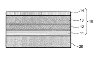
以下、図1及び図2を参照して本発明に係る反射防止膜及び光学素子の実施の形態を説明する。 Hereinafter, an embodiment of an antireflection film and an optical element according to the present invention will be described with reference to FIGS. 1 and 2.
1.反射防止膜10
まず、本件発明に係る反射防止膜10について説明する。本件発明に係る反射防止膜10は、基材20上に順次積層される中間層12と、低屈折率層13とを備え、光学干渉作用により入射光の反射を防止するものである。基材20と中間層12との間には、図1に示すように無機材料から成る無機下地層11を備えることができる。本件発明において、低屈折率層13は、図2(a)、(b)に示すように、中空シリカ粒子131がバインダ132で結着された構成を有している。本件発明では、基材20上に、当該バインダ132との密着性のよい有機金属化合物を主成分とし、低屈折率層13を成膜する際に用いる塗工液に対して濡れ性を有する中間層12を設け、この中間層12の表面に低屈折率層13を成膜することにより、湿式成膜法で成膜される低屈折率層13の成膜性及び基材20との密着性を向上したものである。以下、基材20及び反射防止膜10を構成する各層について順に説明する。
1.
First, the
(1)基材20
まず、反射防止膜10が設けられる基材20について説明する。本件発明では、当該反射防止膜10が設けられる基材20として光学素子基材を用いることができる。光学素子基材は、ガラス製であってもよいし、プラスチック製であってもよく、その材質に特に限定はない。例えば、レンズ、プリズム(色分解プリズム、色合成プリズム等)、偏光ビームスプリッター(PBS)、カットフィルタ(赤外線用、紫外線用等)など各種の光学素子基材20を用いることができる。本件発明では、上述した通り、中間層12の表面に低屈折率層13を設けるため、湿式成膜法を採用する場合であっても、レンズ曲率の大きい小型のレンズ等についても低屈折率層13を良好に成膜することができ、その密着性も優れたものとすることができる。このため、このような小型レンズについても基材20として良好に用いることができる。
(1)
First, the
(2)無機下地層11
次に、無機下地層11について説明する。本件発明では、上述したとおり、基材20と中間層12との間に無機下地層11を設けることができる。無機下地層11は無機材料から成る層であり、光学干渉層として機能する。光学干渉層とは、入射光に対する界面反射光の位相変化を所定の値とすべく、薄膜の特性マトリックスに基づいて、屈折率と光学膜厚とが所定の値になるように光学設計された光学薄膜をいう。
(2)
Next, the
ここで、無機材料としては、屈折率が1.35以上2.5以下の透明無機材料を用いることが好ましい。このような透明無機材料として、例えば、Al2O3、ZrO2+Al2O3、SiN、SiC、SiO、MgO、La2O3+Al2O3、Y2O3、In2O3+SnO2、La2Ti2O7、SnO2、Ta2O5、HfO2、ZrO2、CeO2、WO3、ZrO2+TiO2、Ta2O5、Ta2O5+ZrO2、Ta2O5+TiO2、Ti3O5、Ti4O7、TiPr6O11+TiO2、TiO、TiO2、Nb2O5、TiO2+La2O3、Pr6O11+TiO2、SiO2、SiOxNy、CeO2、MgF2、ZnS、YF3を挙げることができる。
Here, as the inorganic material, it is preferable to use a transparent inorganic material having a refractive index of 1.35 to 2.5. As such a transparent inorganic material, for example, Al 2 O 3 , ZrO 2 + Al 2 O 3 , SiN, SiC, SiO, MgO, La 2 O 3 + Al 2 O 3 , Y 2 O 3 , In 2 O 3 + SnO 2 , La 2 Ti 2 O 7 , SnO 2 , Ta 2 O 5 , HfO 2 , ZrO 2 , CeO 2 , WO 3 , ZrO 2 + TiO 2 , Ta 2 O 5 , Ta 2 O 5 + ZrO 2 , Ta 2 O 5 + TiO 2 , Ti 3 O 5 , Ti 4 O 7 , TiPr 6 O 11 + TiO 2 , TiO, TiO 2 , Nb 2 O 5 , TiO 2 + La 2 O 3 , Pr 6 O 11 + TiO 2 , SiO 2 , SiO x N y , mention may be made of CeO 2, MgF 2, ZnS,
無機下地層11は、無機材料からなるサブ層(薄層)を1層以上積層した単層膜又は多層膜であることが好ましい。ここで、サブ層とは、無機下地層11を構成する物理的な一層を指す。本件発明では、無機下地層11を少なくとも1層以上のサブ層を積層した構成とし、各々のサブ層をそれぞれ光学干渉層として機能させることにより、当該反射防止膜10の反射率を極めて低くすることができる。
The
無機下地層11を単層膜とする場合であっても、多層膜とする場合であっても、各層の光学設計(屈折率、光学膜厚の設計)は、通常の反射防止膜を設計する場合と同様にマトリクス法により行うことができる。無機下地層11を構成するサブ層の積層数を増やすことにより、より高い反射防止性能をもつ反射防止膜10を得ることができる。
Whether the
より広帯域、且つ、より低反射の反射防止膜10を得るには、各サブ層の光学膜厚を150nm以下とすることが好ましい。各サブ層の光学膜厚が150nmを超える場合、必要のないリップルの多い設計となり当該反射防止膜10の平均反射率を低く保つことができないため、好ましくない。
In order to obtain the
無機下地層11(各サブ層)を成膜する際には、真空成膜法を採用することが好ましい。無機下地層11を、真空成膜法により基材20の表面に成膜することにより、無機下地層11を基材20の表面に対して強固に密着させることができる。真空成膜法として、物理蒸着法及び化学蒸着法のいずれも好適に用いることができる。物理蒸着法としては、真空蒸着法、スパッタ法、イオンプレーティング法、イオンビーム蒸着法を挙げることができる。また、化学蒸着法としては、CVD法(プラズマCVD法を含む)を挙げることができる。これらの中でも、特に、真空蒸着法、スパッタ法、CVD法を好適に採用することができる。これらの方法を採用することにより、1nm以上150nm以下の範囲の物理膜厚の無機下地層11(若しくはサブ層)を精度よく成膜することができる。
When forming the inorganic underlayer 11 (each sublayer), it is preferable to employ a vacuum film forming method. By depositing the
(3)中間層12
次に、中間層12について説明する。中間層12は、低屈折率層13の層構成材料の一つであるバインダ132との密着性が良好な有機金属化合物を主成分とし、低屈折率層13の層構成材料(中空シリカ粒子131、バインダ132)を含む塗工液に対して濡れ性を有する層である。
(3)
Next, the
ここで、有機金属化合物とは、分子中に少なくとも一つの金属−炭素結合を有する化合物を指し、金属と有機基が金属−炭素の直接結合により結びついた化合物をいう。また、バインダ132との密着性が良好な有機金属化合物とは、主として、バインダ132との密着性の良好な有機基を有する有機金属化合物を指し、具体的には、メチル基、エチル基、n?プロピル基、イソプロピル基、ブチル基、イソブチル基、tert?ブチル基、ヘキシル基、シクロヘキシル基、オクチル基、ノルボルニル基、イソノルボルニル基等のアルキル基、ビニル基、アリル基、プロペニル基、ブテニル基等のアルケニル基、フェニル基、トリル基等のアリール基、ベンジル基、フェニルエチル基等のアラルキル基、メトキシ基、エトキシ基、プロポキシ基、イソプロポキシ基、ブトキシ基、イソブトキシ基、tert?ブトキシ基などのアルコキシル基、その他としてアミド基、イミド基、ニトリル基、カルボニル基、カルボキシル基、ヒドロキシ基等を有する有機金属化合物を指す。例えば、これらの有機基を有する 中間層12内において、これらの有機基が互いに化学的に結合(架橋重合)した高分子網目構造を形成していてもよい。
Here, the organometallic compound refers to a compound having at least one metal-carbon bond in a molecule, and refers to a compound in which a metal and an organic group are linked by a metal-carbon direct bond. The organometallic compound having good adhesion to the
また、本件発明では、中間層12には、無機下地層11又は基板20との良好な密着性と、光学的に可視域で強い吸収を示さないことが求められる。これらの観点から、中間層12を構成する有機金属化合物に含まれる金属元素は、2族の金属元素(Mg、Ca、Ba)、3族の金属元素(Y)、ランタノイド(La、Ce、Pr)、4族の金属元素(Ti、Zr、Hf)、5族の金属元素(Ta、Nb)であることが好ましく、卑金属であるIn、Ga、Sn、半導体であるSi等であってもよい。なお、Siは厳密には金属ではないが、有機ケイ素化合物は有機金属化合物に含まれるものとして一般に取り扱われている。従って、本件発明では、上述した有機基とこれらの元素(金属元素)から成る化合物を有機金属化合物と称するものとする。
Moreover, in this invention, it is calculated | required that the intermediate |
本件発明では、上記塗工液との濡れ性が良好な中間層12を得ることができるという観点から、中間層12を構成する有機金属化合物は、有機ケイ素化合物、又は、4族の金属元素を含む有機金属化合物であることが好ましく、有機ケイ素酸化物、又は、4族の金属元素を含む有機金属酸化物であることがより好ましい。これらの有機金属化合物は、材料自体において上記塗工液に対して濡れ性を有するか、或いは、中間層12を成膜した後に、後述する表面処理を施すことにより当該塗工液に対する濡れ性を付与することができる。
In the present invention, from the viewpoint that the
ここで、上記塗工液との濡れ性を有するとは、当該中間層12に対する上記塗工液の接触角が45°未満であることをいい、当該接触角が低いほど、上記塗工液が中間層12の表面に良く濡れ、中間層12の表面にムラの無い、均一な低屈折率層13を成膜することができるようになる。これと同時に、中間層12と低屈折率層13との密着性もより良好なものとすることができる。当該観点から、当該接触角は、30°以下であることが好ましく、10°以下であることが好ましく、5°以下であることがさらに好ましい。
Here, having wettability with the coating solution means that the contact angle of the coating solution with respect to the
また、中間層12には、上記塗工液に対する濡れ性を向上するための表面処理が施されていることが好ましい。当該表面処理を中間層12に施すことにより、中間層12に対する上記塗工液の濡れ性をより良好にすることができる。具体的には、プラズマ処理、UV洗浄処理等を中間層12の表面に施すことにより、中間層12の表面の濡れ性を向上することができる。
In addition, the
例えば、中間層12を真空成膜法により成膜した場合、チャンバーをリークせずに、アルゴンガス、水素ガス、ヘリウムガス、酸素ガス等を処理ガスとし、中間層12の表面にプラズマを照射する方法を採用することができる。当該方法によれば、中間層12を成膜する際に用いた真空成膜装置を用いて、成膜後、直ちに表面処理を施すことができるため好ましい。
For example, when the
また、中間層12の成膜後、大気圧プラズマ処理、UV洗浄処理等により、中間層12の表面に濡れ性を向上してもよい。例えば、湿式成膜法により中間層12を形成する場合、減圧装置を要しないという観点から、大気圧プラズマ処理、或いはUV洗浄処理等により中間層12に対して表面処理を施すことが好ましい。
Further, after the
但し、中間層12に対する上記塗工液の接触角は、表面処理の有無によらず、上述の範囲内であることが好ましい。
However, the contact angle of the coating liquid with respect to the
次に、中間層12の物理膜厚について述べる。中間層12の物理膜厚は、1nm以上150nm以下であることが好ましい。中間層12の物理膜厚が1nm未満である場合、凹凸曲面を有するレンズ等を基材20として採用した場合、このような凹凸曲面に対して、当該中間層12を均一に、且つ、ムラ無く成膜することは困難である。その結果、中間層12の表面に対して低屈折率層13の成膜が困難になり、低屈折率層13と中間層12を介して基材20の表面に密着させることが困難になる。ただし、後述する自己組織化単分子膜(SAM膜)は単分子層で均一に表面を被覆することができるため、その限りではない。一方、中間層12の物理膜厚が150nmを超える場合、光学干渉層としての中間層12に要求される光学特性を満たすように膜設計を行うことが困難になる。すなわち、上記位相変化が適切な値となるように反射防止膜10の光学設計を行うことが困難になり、その結果、反射防止膜10の反射防止性能の低下を招く恐れがあり、好ましくない。当該観点から、中間層12の物理膜厚は120nm以下であることがより好ましく、100nm以下であることが更に好ましい。
Next, the physical film thickness of the
中間層12の屈折率は、1.30以上2.35以下の範囲内であることが好ましい。有機金属化合物膜を中間層12とする場合、中間層12の屈折率は概ね当該範囲内の値を示す。中間層12の物理膜厚が30nm以下である場合、当該中間層12は、反射防止膜10全体の光学特性に殆ど影響を及ぼさないため、中間層12の屈折率は上記範囲内であれば、任意の値であってもよい。
The refractive index of the
一方、中間層12を光学干渉層として機能させる場合、低屈折率層13の屈折率をn(1)、基材20を屈折率n(sub)とした場合、中間層12の屈折率n(2)は下記式(1)の関係を満たすことが好ましい。
On the other hand, when the
中間層12の屈折率n(2)が、基材20の屈折率n(sub)と、低屈折率層13の屈折率n(1)とに基づいて、上記範囲内となる場合、当該反射防止膜10の光学的な層構成を中間層12と低屈折率層13の二層構造とする場合であっても、当該反射防止膜10の反射防止性能を極めて高いものとすることができる。なお、当該反射防止膜10が無機下地層11を備える場合には、中間層12の屈折率や膜厚は、マトリクス法により(光学特性を)適宜設計することが好ましい。
When the refractive index n (2) of the
次に、中間層12の成膜方法について説明する。中間層12を成膜する方法は特に限定されるものではない。例えば、上述した様に、真空成膜法、湿式成膜法等を好適に採用することができる。
Next, a method for forming the
1)真空成膜法
真空成膜法は、無機下地層11において説明した方法と同様の方法を採用することができる。当該方法を採用することにより、膜厚の制御が容易であり、中間層12の物理膜厚が1nm以上150nm以下となるように、中間層12の物理膜厚を制御よく成膜することができる。従って、中間層12を上述のように光学干渉層として機能させる場合、中間層12の膜厚を精度よく制御することができるという観点から、当該真空成膜法を採用することが好ましい。
1) Vacuum Film Formation Method For the vacuum film formation method, a method similar to the method described for the
本件発明では、中間層12を真空成膜法により成膜する際には、特に、化学蒸着法(CVD法)を採用することが好ましい。化学蒸着法は、薄膜構成材料(中間層12を構成する成分)の構成元素を含む化合物を原料ガスとし、当該原料ガスをチャンバー内に供給し、気相または基板表面での化学反応により薄膜を形成する方法である。本件発明では、薄膜構成材料として目的とする有機金属化合物の構成元素を含む化合物を原料ガスとする。CVD法によれば、酸素ガスを導入しながら成膜することにより、酸素を含まない化合物を上記薄膜構成材料として用いた場合であっても、有機金属酸化物を主成分とする層を得ることができる。また、同じ薄膜構成材料を用いた場合であっても、導入する酸素ガスの量を原料ガスに対して適宜変化させる等、成膜条件を適宜調整することにより、中間層12の屈折率を変化させることができる。中間層12を光学干渉層として機能させる場合、膜厚及び屈折率の制御が容易であることから、化学蒸着法を採用することが好ましい。
In the present invention, when the
また、中間層12を化学蒸着法により成膜する際には、特に、プラズマCVD法を採用することが好ましい。プラズマCVD法によれば、上述したように、中間層12成膜後、チャンバーをリークせずに中間層12の表面にプラズマを照射して、中間層12の表面の濡れ性を向上することができるため、濡れ性の良好な中間層12を効率的に得ることができる。
In addition, when the
プラズマCVD法により、有機金属化合物を主成分とする中間層12を成膜する際の層構成材料として、以下のものを用いることができる。
The following materials can be used as a layer constituting material when forming the
有機ケイ素化合物を主成分とする中間層12を成膜する場合、有機ケイ素化合物の構成元素を含む化合物を上記薄膜構成材料として用いる。具体的には、薄膜構成材料として、アルキルシラン、アルコキシシラン、アルキルシラザン等を用いることができる。また、アルキルシランとして、具体的には、テトラメチルシラン(TMS)等、アルコキシシランとして、ヘキサメチルジシロキサン(HMDSO)、テトラエトキシシラン(TEOS)等、アルキルシラザンとしてヘキサメチルジシラザン(HMDS)等を用いることができる。また、これら以外にもトリメトキシシラン、トリプロポキシシラン、トリブトキシシラン、メチルジメトキシシラン、メチルジエトキシシラン、メチルジプロポキシシラン、メチルジブトキシシラン、エチルジメトキシシラン、エチルジエトキシシラン、エチルジプロポキシシラン、エチルジブトキシシラン、プロピルジメトキシシラン、プロピルジエトキシシラン、プロピルジプロポキシシラン、プロピルジブトキシシラン、i-プロピルジメトキシシラン、i-プロピルジエトキシシラン、i-プロピルジプロポキシシラン、i-プロピルジブトキシシラン、ブチルジメトキシシラン、ブチルジエトキシシラン、ブチルジプロポキシシラン、ブチルジブトキシシラン、i-ブチルジメトキシシラン、i-ブチルジエトキシシラン、i-ブチルジプロポキシシラン、i-ブチルジブトキシシラン、s-ブチルジメトキシシラン、s-ブチルジエトキシシラン、s-ブチルジプロポキシシラン、s-ブチルジブトキシシラン、フェニルジメトキシシラン、フェニルジエトキシシラン、フェニルジプロポキシシラン、フェニルジブトキシシラン、ジメチルメトキシシラン、ジメチルエトキシシラン、ジメチルプロポキシシラン、ジメチルブトキシシラン、メチルエチルメトキシシラン、メチルエチルエトキシシラン、メチルエチルプロポキシシラン、メチルエチルブトキシシラン、ジエチルメトキシシラン、ジエチルエトキシシラン、ジエチルプロポキシシラン、ジエチルブトキシシラン、メチルプロピルメトキシシラン、メチルプロピルエトキシシラン、メチルプロピルプロポキシシラン、メチルプロピルブトキシシラン、ジプロピルメトキシシラン、ジプロピルエトキシシラン、ジプロピルプロポキシシラン、ジプロピルブトキシシラン等を用いることができる。これらの薄膜構成材料を用いて、例えば、酸素ガスを導入しながらCVD法により基材20上(若しくは無機下地層11上)に中間層12を成膜すると、有機ケイ素酸化物を主成分とする中間層12を得ることができる。
When forming the
例えば、ヘキサメチルジシロキサンを薄膜構成材料(原料ガス)とし、CVD法により成膜した場合、導入する酸素ガスの量等に応じて、1.4以上1.65以下の範囲内の屈折率を有する有機ケイ素酸化物膜を得ることができる。例えば、低屈折率層13の屈折率が1.17以上1.24以下の範囲内である場合、上記式(1)を満たす範囲内の屈折率を有する中間層12を形成することができる。また、ヘキサメチルジシラザンを原料ガスとして用いた場合、中間層12の表面の上記接触角を安定に維持することができ、塗工液に対する濡れ性が極めて良好になる。このため、低屈折率層13の成膜性及び密着性がより良好になるため好ましい。
For example, when hexamethyldisiloxane is used as a thin film constituent material (raw material gas) and a film is formed by a CVD method, the refractive index is in the range of 1.4 to 1.65 depending on the amount of oxygen gas to be introduced and the like. An organic silicon oxide film can be obtained. For example, when the refractive index of the low
4族の金属元素を有する有機金属化合物を主成分とする中間層12を成膜する場合、4族の金属元素を有する有機金属化合物の構成元素を含む化合物を上記薄膜構成材料として用いることができる。具体的には、有機チタン化合物、有機ジルコニウム化合物等を用いることができ、有機チタン酸化物、有機ジルコニウム酸化物を用いることが好ましい。例えば、チタンイソプロポキシド(TPT)、テトラプロキシチタン、松本製薬工業株式会社製のオルガニックチタン等を層構成材料として用いることにより、有機チタン化合物を主成分とする中間層12を得ることができる。この場合、成膜後に熱処理を施すことにより、熱処理条件等に応じて 屈折率が1.7以上2.25以下の範囲内の有機チタン化合物から成る中間層を得ることができる。また、松本製薬工業株式会社製のオルガニックジルコニア等を層構成材料として用いることにより、有機ジルコニウム化合物を主成分とする中間層12を得ることができる。
When forming the
2)湿式成膜法
次に、湿式成膜法について説明する。中間層12を成膜する際に、湿式成膜法を採用する場合、ディップコート法、スピンコート法、スプレーコート法、ロールコーティング法、スクリーン印刷法を採用することができる。基材20の形状、成膜する膜厚等に応じて、適宜、適切な手法を採用することができる。これらの方法は、従来公知の方法等を適宜採用することができる。例えば、エチルトリメトキシシラン、メチルトリメトキシシラン、メチルトリエトキシシラン、ヘキシルトリメトキシシラン、オクタデシルトリメトキシシラン、オクタデシルトリエトキシシラン、ビニルトリメトキシシラン、ビニルトリエトキシシラン、フェニルトリメトキシシラン、フェニルトリエトキシシラン、3−アミノプロピルトリエトキシシラン、3−メタクリロキシプロピルトリメトキシシラン、3−メタクリロキシプロピルトリエトキシシラン、N−(2−アミノエチル)−3−アミノプロピルトリメトキシシラン、3−クロロプロピルトリメトキシシラン、3−(N,N−ジグリシジル)アミノプロピルトリメトキシシラン、3−グリシドキシシプロピルトリメトキシシランやジメチルジメトキシシラン、ジメチルジエトキシシラン、ジフェニルジメトキシシラン、ジフェニルジエトキシシラン、メチルフェニルジメトキシシラン、メチルビニルジメトキシシラン、メチルビニルジエトキシシラン、3−グリシドキシプロピルメチルジメトキシシラン、3−アミノプロピルメチルジメトキシシラン、N−(2−アミノエチル)−3−アミノプロピルメチルジメトキシシラン、3−クロロプロピルメチルジメトキシシラン、3−クロロプロピルメチルジエトキシシラン、シクロヘキシルメチルジメトキシシラン、ヘプタデカフルオロデシルメチルジメトキシシラン、3−メタクリロキシプロピルジメトキシシラン、オクタデシルメチルジメトキシシラン等を用いることにより、有機ケイ素化合物から成る中間層12を得ることができる。
2) Wet deposition method Next, a wet deposition method will be described. When the
また、本件発明では、中間層12を有機金属化合物から成る自己組織化単分子膜とすることも好ましい。自己組織化単分子膜とは、膜形成面材料と化学的に結合した単分子膜をいい、分子間の相互作用により膜形成面に分子が密に吸着し、分子の配向性が揃った膜をいう。例えば、ディップコート法等の湿式成膜法により、このような自己組織化単分子膜を得ることができる。
In the present invention, it is also preferable that the
自己組織化単分子膜の厚さは、中間層12を構成する有機金属化合物の単分子長と略同じ厚さになり、その厚みは均一なものとなる。このため、中間層12を自己組織化単分子膜として構成することにより、膜厚が精密に制御され、均一な厚みの中間層12を再現性よく安定に成膜することができる。さらに、中間層12層と低屈折率層13の塗工液との濡れ性が向上することにより、低屈折率層13の成膜性が向上し、表面欠陥に伴う膜の外観不良が発生するのを防止することができる。
The thickness of the self-assembled monomolecular film is substantially the same as the monomolecular length of the organometallic compound constituting the
また、自己組織化単分子膜の膜厚は、上述の通り、中間層12を構成する有機金属化合物の単分子長と略同じ厚さとなり、基材20の形状によらず、均一な膜厚の中間層12を得ることができる。例えば、炭素分子18個を直鎖とするオクタデシル基の長さは2.5nmである。この場合、基材20の形状に追随するように2.5nmの均一な膜厚の中間層12を得ることができる。中間層12がこのように極薄い層として構成された場合、当該中間層12は反射防止膜10全体の光学特性に殆ど影響を与えなくなる。すなわち、この場合、中間層12には光学干渉層としての機能は無視することができる。従って、中間層12を基材20の種類や、要求される反射防止性能等に応じて光学設計する必要がなくなる。このため、例えば、多品種のレンズを製造する際に、レンズの種類によらず中間層12の形成工程を共通化することができる。
Further, as described above, the film thickness of the self-assembled monomolecular film is substantially the same as the monomolecular length of the organometallic compound constituting the
湿式成膜法により、有機金属化合物から成る自己組織化単分子膜を成膜可能な材料として、ヘキサメチルジシラザン、トリクロロオクタデシルシラン、日本曹達株式会社製のSAMLAY(登録商標)、東京応化工業株式会社製のOSRA(登録商標)などを挙げることができる。また、これら以外でもトリクロロアルキルシランやアルキルシラノール等を用いることにより自己組織化単分子膜を形成することができる。これらの材料を用いて、ディップコート法、或いはスピンコート法等の湿式成膜法により有機ケイ素化合物の自己組織化単分子膜を得ることができる。なお、ヘキサメチルジシラザンやOSRAは、蒸着法によっても自己組織化単分子膜を成膜することができる。 As materials capable of forming self-assembled monolayers composed of organometallic compounds by wet film formation, hexamethyldisilazane, trichlorooctadecylsilane, SAMLAY (registered trademark) manufactured by Nippon Soda Co., Ltd., Tokyo Ohka Kogyo Co., Ltd. Examples include OSRA (registered trademark) manufactured by the company. Besides these, a self-assembled monolayer can be formed by using trichloroalkylsilane, alkylsilanol, or the like. Using these materials, a self-assembled monolayer of an organosilicon compound can be obtained by a wet film formation method such as a dip coating method or a spin coating method. Note that hexamethyldisilazane and OSRA can form a self-assembled monolayer by vapor deposition.
3) その他
その他、中間層12を成膜する際には、上述した以外の方法についても適宜採用することができ、例えば、熱加水分解による方法や、原子層堆積装置(ALD装置)等を用いて中間層12を成膜してもよい。
3) Other In addition, when the
(4)低屈折率層13
次に、低屈折率層13について説明する。低屈折率層13は、既に述べた通り、上記低屈折率層13上に湿式成膜法により成膜される層であり、中空シリカ粒子131が前記バインダ132により結着されて成る層である。
(4) Low
Next, the low
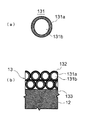
本件発明において、中空シリカ粒子131とは、バルーン構造(中空構造)を有するシリカ粒子を指し、具体的には、図2(a)に模式的に示すように、シリカから成る外殻部131aと、この外殻部131aに周囲が完全に囲まれた中空部131bとから構成されたシリカ粒子を指す。本件発明では、低屈折率層13の構成成分として、中空部131bを有する中空シリカ粒子131を主たる成分として採用することにより、低屈折率層13の屈折率をシリカ自体の屈折率(1.48)よりも低減可能とした。また、シリカ粒子内に細孔を多数有する多孔質シリカの集合体から構成された多孔質シリカ層等に比して、図2(b)に示すように、外殻部131aにより周囲が完全に包囲された中空シリカ粒子131をバインダ132により結着した層とすることにより、当該低屈折率層13を低屈折率層13に強固に密着させて、耐擦傷性や耐久性に優れた反射防止膜10とすることができる。
In the present invention, the
ここで、本件発明において、中空シリカ粒子131は、バインダ132によりその外側(外殻部131aの外側)が被覆された状態で、互いに結着されていることが好ましい。中空シリカ粒子131の外側がバインダ132により被覆された状態で、中空シリカ粒子131同士が互いにバインダ132を介して結着されることにより、低屈折率層13との密着性が増す。これに伴い、反射防止膜10の耐久性や耐擦傷性も向上する。また、中空シリカ粒子131の外側をバインダ132により被覆することにより、中空シリカ粒子131内の中空部131bや、低屈折率層13内の空隙部143に対して、水や他の液体が吸着するのを抑えることができる。
Here, in the present invention, it is preferable that the
以上のように構成された低屈折率層13において、その屈折率は、1.15以上1.24以下であることが好ましい。低屈折率層13の屈折率が1.15未満である場合、中空シリカ粒子131をバインダ132により被覆し、且つ、中空シリカ粒子131をバインダ132により被覆した状態で十分に結着することが困難になる。従って、低屈折率層13の屈折率が1.15未満の場合、低屈折率層13の耐久性等が低下するため、好ましくない。当該観点から、低屈折率層13の屈折率は1.17以上であることがより好ましい。一方、低屈折率層13の屈折率が1.24を超える場合は、設計中心波長における反射率が高くなるため好ましくない。従って、当該観点から、低屈折率層13の屈折率は上記範囲内において低い方が好ましく、1.23以下であることがより好ましい。
In the low
また、低屈折率層13内には、図2(b)に示すように、中空シリカ粒子131の中空部131b以外の空隙部143が存在することが好ましい。低屈折率層13内に、中空シリカ粒子131内の中空部131b以外の空隙部143が存在することにより、低屈折率層13の屈折率をシリカ自体の屈折率よりも更に低減することができる。本件発明では、空隙部143をバインダ材等により充填しなくとも、上述した通り、中間層12を介して、基材20と、低屈折率層13とを強固に密着させることができる。
In addition, as shown in FIG. 2B, it is preferable that a void portion 143 other than the
低屈折率層13において中空シリカ粒子131が占める体積は、30体積%以上99体積%以下であることが好ましい。ここでいう中空シリカ粒子131が占める体積とは、低屈折率層13において、中空シリカ粒子131の外殻部131aと、この中空部131bに囲まれる中空部131bとを含む中空シリカ球の全体積を意味する。低屈折率層13において中空シリカ粒子131が占める体積が30体積%未満である場合、低屈折率層13の耐久性や耐擦傷性が低下するため好ましくない。また、中空シリカ粒子131の占める体積が30体積%未満である場合、低屈折率層13においてバインダ132が占める体積率が増加する。その結果、低屈折率層13の屈折率を上記範囲内の値になるようにすることが困難になる場合がある。これらの観点から、低屈折率層13において中空シリカ粒子131が占める体積は60体積%以上であるとより好ましい。一方、低屈折率層13において中空シリカ粒子131が占める体積が99体積%を超える場合、中空シリカ粒子131同士を結着するバインダ132が占める体積比が低く、中空シリカ粒子131同士を十分に結着することができず、その結果、低屈折率層13を形成することが困難になる。中空シリカ粒子131同士を十分に結着し、低屈折率層13内に存在する空隙部133の比率を増加させるという観点から、低屈折率層13において中空シリカ粒子131が占める体積は90体積%以下であることがより好ましい。
The volume occupied by the
低屈折率層13の層構成材料としての中空シリカ粒子131は、その平均粒径D50が5nm以上100nm以下であることが好ましい。中空シリカ粒子131の平均粒径D50が5nm未満である場合、低屈折率層13内に中空シリカ粒子131の中空部131b以外の空隙部133を設けることが困難になる。一方、中空シリカ粒子131の平均粒径が100nmを超える場合、光の散乱(ヘイズ)が発生する場合があり好ましくない。光の散乱が発生した場合、当該中空シリカ粒子131を用いた反射防止膜10は、撮像素子に要求される反射防止性能を満たすことができず、好ましくない。さらに、中空シリカ粒子131の平均粒径が100nmを超える場合、低屈折率層13の物理膜厚を数nm単位で精密に制御することが極めて困難になる。
一方、バインダ132としては、樹脂材料又は金属アルコキシドを採用することができる。樹脂材料としては、例えば、エポキシ樹脂、アクリル樹脂、フッ素樹脂、シリコーン樹脂、シクロオレフィン樹脂(例えば、ZEONEX(登録商標)等或いはこれらの単量体化合物を挙げることができる。これらの樹脂材料は紫外線硬化性、常温硬化性、又は熱硬化性の化合物であることが好ましく、特に紫外線硬化性又は常温硬化性の化合物であることが好ましい。樹脂基材等の熱膨張係数の高い基材20を用いる場合に、熱処理を行わなくとも低屈折率層13の形成が可能であれば、基材20の熱膨張変形を防止することができるためである。具体的な層形成方法として、例えば、これらの材料と、中空シリカ粒子131とを混合して、必要に応じて重合開始剤や架橋剤等を添加し、溶剤等により適切な濃度に希釈して塗工液を調製し、ディップコート法、スピンコート法、スプレー法、ロールコーティング法、スクリーン印刷法等の湿式法を採用することができる。これらの方法により無機下地層11の表面に塗工液を適切な厚みとなるように塗布し、その後、紫外線照射、或いは熱処理を施すことなどにより重合架橋して、溶媒を揮発させること等により低屈折率層13を形成することができる。
On the other hand, as the
また、金属アルコキシドを溶媒に溶解または懸濁して、ゾルを形成し加水分解・重合によりゲルが生成される材料であることが好ましく、例えば、アルコキシシラン又はシルセスキオキサン等の加水分解・重合によりシリカゲルが生成される材料を用いることが好ましい。これらの材料と、中空シリカ粒子131とを、溶媒に溶解又は懸濁してゾルゲル剤を調製し、無機下地層11の表面にゾルゲル剤をスプレーコート法、スピンコート法、ディップコート法、フローコート法、バーコート法等により塗布し、加水分解により中空シリカ粒子131を含むゲルを作成し、溶媒を揮発させること等により、低屈折率層13を形成することができる。
Further, it is preferably a material in which a metal alkoxide is dissolved or suspended in a solvent to form a sol and a gel is generated by hydrolysis / polymerization. For example, by hydrolysis / polymerization of alkoxysilane or silsesquioxane or the like. It is preferable to use a material from which silica gel is produced. These materials and the
また、低屈折率層13の物理膜厚は、100nm以上180nm以下の範囲内であることが好ましい。低屈折率層13の物理膜厚が100nm未満である場合や180nmを超える場合、上記位相変化を適切な値とすることが困難になり、反射防止膜10の反射防止性能が低下する恐れがあるため、好ましくない。
The physical film thickness of the low
(5)機能層14
本件発明においては、図1に示すように、低屈折率層13の表面に、屈折率が1.30以上2.35以下であり、且つ、物理膜厚が0.1nm以上30nm以下の機能層14を設けてもよい。本件発明に係る反射防止膜10は、基材20上に設けられる中間層12及び低屈折率層13から成る光学的二層構造、又は、無機下地層11、中間層12及び低屈折率層13から成る光学的三層構造を反射防止機能に関する主たる構成としている。機能層14は、これらの光学的二層構造又は光学的三層構造により得られる反射防止性能に光学的な影響を与えない透明な極薄い膜であって、反射防止膜10の表面の硬度、耐擦傷性、耐熱性、耐候性、耐溶剤性、撥水性、撥油性、防曇性、親水性、耐防汚性、導電性等の向上等の機能を有する層を指す。
(5)
In the present invention, as shown in FIG. 1, a functional layer having a refractive index of 1.30 to 2.35 and a physical film thickness of 0.1 nm to 30 nm on the surface of the low
ここで、機能層14の屈折率が1.30以上2.35以下であって、且つ、物理膜厚が0.1nm以上30nm以下であれば、本件発明に係る反射防止膜10による反射防止効果に対する光学的な影響を無視することができる。屈折率が上記範囲を超える場合、当該反射防止膜10の反射防止特性に光学的に影響を及ぼす恐れがある。また、膜厚が1nm未満であると、機能層14を設けても当該機能層14に要求される機能を発揮することができず好ましくない。また、膜厚が30nmを超える場合、屈折率が上記範囲内であっても、当該反射防止膜10の反射防止特性に光学的な影響を及ぼす恐れがあるため、好ましくない。
Here, if the refractive index of the
機能層14を構成する材料としては、屈折率が1.30以上2.35以下の透明材料を用いることができる。屈折率が当該範囲内であって透明な材料であれば、反射防止膜10の表面に付与すべき機能に応じて、適宜、適切な材料を選択すればよい。例えば、屈折率が当該範囲内の透明な無機材料として、SiOxNy/SiO2/SiOx/Al2O3/ZrO2とTiO2との混合物/La2O3とTiO2との混合物/SnO2/ZrO2/La2O3とAl2O3との混合物/Pr2O5/ITO(酸化インジウムスズ)/AZO(酸化亜鉛アルミニウム)などを挙げることができる。また、DLC(ダイアモンドライクカーボン)/HMDSO(ヘキサメチルジシロキサン)/エポキシ系の樹脂/アクリル系の樹脂(特に、PMMA樹脂(ポリメタクリル酸メチル樹脂)/フッ素系の樹脂等を用いることができる。また、これらの材料を含む各種ハードコート剤を用いてもよい。機能層14の形成に際しては、材料及び膜厚に応じて適宜、適切な成膜方法を採用することができる。
As a material constituting the
機能層14を低屈折率層13の表面に設ける場合、低屈折率層13の物理膜厚と機能層14の物理膜厚とを合計した全物理膜厚が100nm以上180nm以下とすることが求められる。この範囲を超えると、当該反射防止膜10の反射防止効果が低下する場合があり好ましくない。
When the
(6)反射率
本件発明に係る反射防止膜10を、無機下地層11、中間層12及び低屈折率層13の光学的三層構造を備える構成とする場合、各層の物理膜厚を上述した好ましい範囲内とすることにより、入射角0度で入射する波長400nm以上800nm以下の光に対する反射率が0.5%以下にすることができ、入射角0度以上45度以下で入射する波長400nm以上700nm以下の光に対する反射率が1.0%以下にすることができる。
(6) Reflectance When the
また、本件発明に係る反射防止膜10を、中間層12及び低屈折率層13の光学的二層構造を備える構成とする場合、中間層12の屈折率n(2)を、基材の屈折率n(sub)及び低屈折率層13の屈折率n(1)に応じて、式(1)の関係を満たすようにすることにより、無機下地層11を備える三層構成の場合と同様の反射防止性能を発揮する。
In addition, when the
但し、当該反射防止膜10を上記光学的二層構造とする場合と、無機下地層11を備える上記光学的三層構造とする場合とを比較すると、無機下地層11を構成するサブ層の積層数を増やすことなどにより、反射防止性能をより向上させることができるため、当該反射防止膜10は無機下地層11を備えることが好ましい。無機下地層11を基材20と、中間層12との間に設けた場合であっても、無機下地層11を真空成膜法により成膜することで、基材20と無機下地層11とを強固に密着させることができ、且つ、中間層12と無機下地層11との密着性も担保することができる。
However, when comparing the case where the
2.光学素子
本件発明に係る光学素子100は、上記記載の反射防止膜10を備えることを特徴とする。光学素子100としては、撮影光学素子や投影光学素子を挙げることができ、具体的には、レンズ、プリズム(色分解プリズム、色合成プリズム等)、偏光ビームスプリッター(PBS)、カットフィルタ(赤外線用、紫外線用等)などを挙げることができる。また、レンズとして、例えば、一眼レフカメラの交換レンズやデジタルカメラ(DSC)に搭載されるレンズ、携帯電話機に搭載されるデジタルカメラ用のレンズ他、各種のレンズが挙げられる。なお、図1に示す光学素子100は、本件発明の一例であり、層構成等を模式的に示したものに過ぎない。
2. Optical Element An optical element 100 according to the present invention includes the
以上説明した上記実施の形態によれば、既に述べた通り、基材20上に、バインダ132との密着性のよい有機金属化合物を主成分とし、低屈折率層13を形成する際に用いられる塗工液に対して濡れ性を有する中間層12を備えるため、低屈折率層13を中間層12の表面に湿式成膜法により良好に成膜することができ、且つ、低屈折率層13を中間層12を介して基材20に密着させることができる。また、中空シリカ粒子131はバインダ132により中間層12に対して良好に密着するため、中空シリカ粒子131の脱落等に伴う低屈折率層12の剥離等を防止することができ、外観の良好な反射防止膜10を製造することができる。また、低屈折率層13の構成成分である中空シリカ粒子131自体は耐久性及び安定性に優れる材料であるため、当該反射防止膜10の耐久性及び安定性を優れたものとすることができる。更に、本件発明に係る反射防止膜10は、各層間或いは基材20との界面において生じる界面反射光を利用して、広い波長範囲及び広い入射角範囲の光線に対して優れた反射防止特性を示す。
According to the above-described embodiment, as described above, the organic metal compound having good adhesion to the
以上説明した本実施の形態は、本件発明に係る反射防止膜10及び光学素子100の一態様であり、本件発明の趣旨を逸脱しない範囲において、適宜変更可能であるのは勿論である。以下、実施例を挙げて本件発明をより具体的に説明するが、本件発明は下記の実施例に限定されるものではない。
The present embodiment described above is an aspect of the
実施例1では、基材20として、株式会社HOYA製のFDS90光学ガラス製のレンズ(屈折率n=1.86)を用いた。そして、この基材20の表面に、表1に示す積層構造を有する反射防止膜10を設けた。具体的には、次のようにして反射防止膜10を作製した。まず、基材20の表面に、無機下地層11をLeybold Optics社製のARES1510を用いて真空蒸着法によって成膜を行った。無機下地層11は、表1に示すように、基材20の表面に極薄膜のAl2O3(反射率n=1.63)と、極薄膜のSiO2(n=1.48)とを順次積層した2層からなる構成とした。無機下地層11を構成する各層の物理膜厚は表1に示す通りである。なお、本件明細書において、単に「SiO2」と記載した場合には、中空構造を有しない通常のシリカを指す。
In Example 1, a lens made of FDS90 optical glass (refractive index n = 1.86) manufactured by HOYA Corporation was used as the
次に、無機下地層11の表面に、Leybold Optics社製のARES1510に付属のプラズマ銃を用いて、プラズマCVD法により有機ケイ素酸化物膜から成る中間層12を成膜した。具体的には、プラズマ銃(APS)により酸素やアルゴンをプラズマ化した雰囲気下に、薄膜構成材料としてのヘキサメチルジシロキサン(HMDSO)ガスを導入し、チャンバー内に設置した基材20の無機下地層11の表面にプラズマ重合反応により生じた有機ケイ素酸化物膜を堆積させた。このとき、チャンバ−内に導入するヘキサメチルジシロキサンガスの流量を200sccm〜500sccm、酸素ガスの流量5sccm〜100sccm、放電電圧90V〜120V、放電電流10A〜30Aの範囲内で、適宜ガス流量及び放電条件を調整することにより、得られるHMDSO膜の屈折率を1.40〜1.65の範囲内で適宜調整することができる。本実施例では、ヘキサメチルジシロキサンガスを400sccm、酸素ガスを10sccm、放電電圧90V、放電電流 20Aとすることにより、表1に示すとおり屈折率が1.54、物理膜厚が47nmの有機ケイ素酸化物膜から成る中間層12を得た。
なお、以下の表1〜表8では、中間層12を構成する成分と共に、中間層12を形成する際に用いた材料を括弧内に表示する。
Next, an
In Tables 1 to 8 below, the materials used when forming the
次に、この中間層12の表面に、低屈折率層13を成膜した。低屈折率層13の成膜に際して、溶剤に中空シリカ粒子131と、バインダ成分としてのアクリル樹脂を溶解、懸濁、調製した塗工液を用いて、ミカサ社製のMS−A150を用いてスピンコート法により塗工膜を成膜した。その後、塗工膜をクリーンオーブンにより90℃で12秒加熱(プレベーク)した後、150℃で1時間加熱(ポストベーク)して、塗工膜中の重合成分の重合架橋を行うと共に溶媒を揮発した。これにより、塗工膜を完全に硬化し、中空シリカ粒子131がアクリル樹脂(バインダ132)で結着して成る低屈折率層13を得た。当該低屈折率層13の屈折率は1.20であり、その物理膜厚は108nmであった。
Next, a low
実施例2では、テトラメチルシラン(TMS)を用いて、有機ケイ素酸化物膜から成る中間層12を成膜した。但し、当該反射防止膜10の層構成及び各層の厚みは表2に示す通りとした。また、無機下地層11及び低屈折率層13は実施例1と略同様にして成膜し、中間層12は、以下のようにして成膜した。
In Example 2, the
中間層12の成膜に際しては、テトラメチルシランを薄膜構成原料として用いた以外は、実施例1と略同様にして、無機下地層11の表面に有機ケイ素酸化物膜を堆積させた。このとき、チャンバ−内に導入するテトラメチルシランガスの流量を10sccm〜200sccm、酸素ガスの流量を5sccm〜200sccm、アルゴンガスの流量5sccm〜200sccm、放電電圧90V〜120V、放電電流10A〜30Aの範囲内で適宜ガス流量及び放電条件を調整することにより、得られる有機珪素酸化物膜の屈折率を1.40〜1.65の範囲内で適宜調整することができる。本実施例では、テトラメチルシランガスを50sccm、酸素ガスを50sccm、アルゴンガスを50sccm、放電電圧を90V、放電電流を20Aとすることにより、表2に示すとおり、屈折率が1.54、物理膜厚が1nmの中間層12を得た。
When the
実施例3では、無機下地層11として、層構成及び各層の厚みを表3に示すとおりとした以外は、実施例1と同様にして反射防止膜10を得た。
In Example 3, the
実施例4では、基材20として、SCHOTT AG社製のN−BK7を採用し、層構成及び各層の厚みを表4に示すとおりとした以外は、実施例1と同様にして実施例4の反射防止膜10を作製した。
In Example 4, N-BK7 manufactured by SCHOTT AG was adopted as the
次に、実施例5の反射防止膜10の製造方法について説明する。実施例5では、基材20として株式会社HOYA製のFDS90光学ガラス製のレンズ(屈折率n=1.86)を用い、表5に示す層構成を有する無機下地層11を実施例1と同様にして成膜した。その後、中間層12の層構成材料としてヘキサメチルジシラザン(HMDS)を用い、有機ケイ素化合物の自己組織化単分子膜から成る中間層12を成膜した。
Next, a method for manufacturing the
具体的には、中間層12は次のように成膜した。無機下地層11を成膜した後の基材20を、ヘキサメチルジシラザン溶液に5〜20分間浸漬させた。これにより、無機下地層11の表面に、ヘキサメチルジシラザン溶液中のヘキサメチルジシラザン分子が化学的に結合・吸着し、分子間力により秩序化されて配向性の揃った自己組織化単分子膜が形成される。その後、イソプロピルアルコール(IPA)を用いた超音波洗浄を行うことにより、無機下地層11の表面にHMDSを原料とする自己組織化膜単分子膜から成る中間層12を成膜した。
Specifically, the
なお、HMDSを用いて自己組織化単分子膜を形成する方法として、以下の方法を採用することもできる。具体的には、恒温槽内にヘキサメチルジシラザン溶液20mlと、表面に無機下地層11を備えた基材20とを設置した後、当該恒温槽を40℃〜60℃に加熱し、約20分間、ヘキサメチルジシラザン溶液を蒸発させる。すると、蒸発したヘキサメチルジシラザンの分子が無機下地層11の表面に結合・吸着し、自己組織化単分子膜が形成される。このような方法によっても、無機下地層11の表面に、上記と同様の自己組織化膜単分子膜(SAM膜)から成る中間層12を成膜することができる。
In addition, the following method is also employable as a method of forming a self-assembled monolayer using HMDS. Specifically, after installing 20 ml of a hexamethyldisilazane solution and a
但し、ヘキサメチルジシラザンと、二酸化ケイ素層(ガラス製の基材20若しくは無機下地層11の最外層)とは、次のように反応する(下記式参照)。二酸化ケイ素層の表面には、ヒドロキシル基(OH基)が存在している。上述のように40℃〜60℃程度で加熱しながら、この二酸化ケイ素層の表面に、ヘキサメチルジシラザン溶液を接触させると、OH基と、ヘキサメチルジシラザン((CH3)3Si−NH−Si(CH3)3)とが熱により反応して、二酸化ケイ素層の表面に−O−Si(CH3)3基を導入することができる。これにより、二酸化ケイ素層の表面に、有機ケイ素酸化物の自己組織化単分子膜が形成される。従って、無機下地層11の表面に有機ケイ素酸化物の自己組織化単分子膜を成膜する際には、無機下地層11の最外層は二酸化ケイ素層であることが好ましい。なお、予め、基材20の表面(無機下地層11が形成されている場合には無機下地層11の表面)を洗浄する等の前処理を施しておくことが好ましいのは勿論である。
However, hexamethyldisilazane and the silicon dioxide layer (the
実施例6では、基材20として、SCHOTT AG社製のN−LAK14を採用し、当該基材20上に無機下地層11を設けずに、直接、基材20の表面に直接中間層12を成膜した。中間層12及び低屈折率層13は、実施例1と略同様にして成膜した。層構成及び各層の厚みは表6に示す通りである。但し、中間層の屈折率は、式(1)の範囲を満たすものとした。∵1.45≦n(2)(=1.52)≦1.54
In Example 6, N-LAK14 manufactured by SCHOTT AG was adopted as the
実施例7では、基材20としてSCHOTT AG社製のN−LAK14を採用した。そして、中間層12として、有機チタン酸化物(有機TiO2)膜を成膜した。反射防止膜10の層構成及び各層の厚みは表7に示す通りとし、無機下地層11及び低屈折率層13は実施例1と同様に成膜した。
In Example 7, N-LAK14 manufactured by SCHOTT AG was used as the
中間層12の成膜に際しては、チタンイソプロポキシドを薄膜構成原料として用い、実施例1と同じ真空成膜装置を用いた。そして、酸素ガス及びアルゴンガスの存在下においてプラズマ銃によりチタンイソプロポキシドを蒸発させて、無機下地層11の表面に有機チタン酸化物膜を堆積させた。このとき、チャンバ−内に導入するチタンイソプロポキシドガスの流量を10sccm〜200sccm、酸素ガスの流量を5sccm〜200sccm、アルゴンガスの流量を5sccm〜200sccm、放電電圧90V〜150V、放電電流10A〜30Aの範囲内でで、適宜ガス量及び放電条件を調整することにより、屈折率が約1.9〜2.1の範囲の耐久性の優れた緻密な有機チタン酸化物膜を成膜することができる。本実施例では、これらの条件を適宜調整することにより、当該無機下地層11の表面に、屈折率が2.10、物理膜厚が1nmの有機チタン酸化物膜から成る中間層12を得た。
In forming the
実施例8では、基材20として、株式会社HOYA製のFDS90光学ガラス製のレンズ(屈折率n=1.86)を用い、中間層12の厚みを160nmとした。当該反射防止膜10の層構成及び各層の厚みは表8に示す通りとし、各層は実施例1と略同様にして成膜した。
In Example 8, a lens made of FDS90 optical glass (refractive index n = 1.86) manufactured by HOYA Corporation was used as the
[比較例1]
比較例1の反射防止膜として、層構成及び各層の厚みを表9に示す通りとし、中間層12を設けなかったこと以外は、実施例1と略同様にして基板20上に反射防止膜を作製した。
[Comparative Example 1]
As the antireflection film of Comparative Example 1, the layer configuration and the thickness of each layer are as shown in Table 9, and the antireflection film was formed on the
[比較例2]
比較例2では、基材20として、SCHOTT AG社製のN−LAK14を用い、層構成及び各層の厚みを表10に示す通りとし、中間層12を設けなかった以外は、実施例1と略同様にして成膜した。
[Comparative Example 2]
In Comparative Example 2, N-LAK14 manufactured by SCHOTT AG was used as the
[評価]
1.評価方法
上記実施例1〜実施例8で得られた各反射防止膜10と、比較例1及び比較例2の反射防止膜の成膜性、密着性及び反射防止特性について評価した。なお、以下において、実施例で作製した反射防止膜10と、比較例で作製した反射防止膜とを同時に指す時は、反射防止膜(10)と記載する。
[Evaluation]
1. Evaluation Method The film forming properties, adhesion, and antireflection characteristics of the
(1)成膜性
上記各反射防止膜(10)の成膜性を、反射防止膜(10)の外観により評価した。反射防止膜10を成膜した後の上記各反射防止膜(10)の外観をそれぞれ目視により評価した。
(1) Film forming property The film forming property of each antireflection film (10) was evaluated by the appearance of the antireflection film (10). The appearance of each antireflection film (10) after forming the
(2)密着性
上記各反射防止膜(10)の密着性を、反射防止膜(10)の膜強度により評価した。膜強度の評価に際しては、椿本工業株式会社製のアルティワイプを用いて、所定の荷重を付加して、各反射防止膜(10)の表面を往復で10回擦ったときの、各反射防止膜(10)の外観の変化の有無をそれぞれ観察した。但し、各反射防止膜(10)の表面を擦るときの荷重は、20g、100g、500gとした。なお、荷重20gは、反射防止膜(10)の表面をなでる程度の負荷に等しく、荷重100gは、反射防止膜(10)の表面を軽く拭く程度の負荷に等しく、荷重500gは、反射防止膜(10)の表面を強く拭く程度の負荷に等しい。
(2) Adhesion The adhesion of each antireflection film (10) was evaluated by the film strength of the antireflection film (10). In the evaluation of the film strength, each antireflection film when the surface of each antireflection film (10) is rubbed 10 times in a reciprocating manner by applying a predetermined load using an Ulti wipe manufactured by Enomoto Kogyo Co., Ltd. The presence or absence of the change in appearance of (10) was observed. However, the load when rubbing the surface of each antireflection film (10) was 20 g, 100 g, and 500 g. The load 20 g is equivalent to a load that strokes the surface of the antireflection film (10), the load 100 g is equivalent to a load that gently wipes the surface of the antireflection film (10), and the load 500 g is the antireflection film. It is equal to the load of wiping the surface of (10) strongly.
(3)反射防止特性
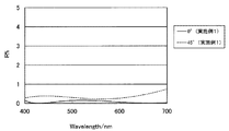
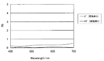
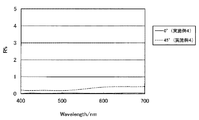
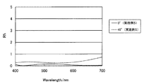
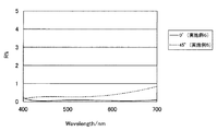
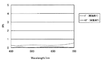
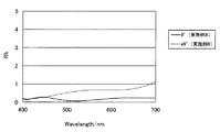
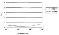
上記各反射防止膜(10)に対する光線の入射角を0度及び45度とし、各入射角において入射光の波長域を400〜700nmの範囲で、各反射防止膜(10)の分光反射率を測定した。分光反射率の測定に際しては、株式会社日立ハイテクノロジーズ社製の分光光度計U4000を用いた。
(3) Anti-reflective properties Each of the anti-reflective films (10 ) Was measured. When measuring the spectral reflectance, a spectrophotometer U4000 manufactured by Hitachi High-Technologies Corporation was used.
2.評価結果
(1)成膜性
表11に、各実施例及び各比較例で作製した反射防止膜(10)の外観を評価した結果を示す。表11において、「○」は反射防止膜(10)の外観が良好であることを示し、「△」は外観が良好でないことを示している。表11に示すように、中間層12を設けなかった、いずれの比較例1、2の反射防止膜も外観が良好でないことが確認された。これに対して、中間層12を設けた実施例1〜8の反射防止膜10は、何れも外観が良好であることが確認された。このことから、低屈折率層13を中間層12の表面に設けることにより、湿式成膜法で成膜される低屈折率層13の成膜性が向上し、外観上、ムラのない均一な反射防止膜10が得られることがわかる。これに対して、中間層12を設けなかった場合には、基材20又は無機下地層11に対して、湿式成膜法で成膜される低屈折率層13の塗工液の濡れ性が悪く、低屈折率層13を秀麗に成膜することができず、その結果、低屈折率層13の成膜性も低下し、反射防止膜の外観も劣化した。
2. Evaluation Results (1) Film Formability Table 11 shows the results of evaluating the appearance of the antireflection film (10) produced in each example and each comparative example. In Table 11, “◯” indicates that the appearance of the antireflection film (10) is good, and “Δ” indicates that the appearance is not good. As shown in Table 11, it was confirmed that any of the antireflection films of Comparative Examples 1 and 2 in which the
(2)密着性
表11に、各実施例及び各比較例で作製した反射防止膜(10)の膜強度を評価した結果を示す。表11において、「○」は当該評価試験の前後において外観に変化が見られなかったことを示す。すなわち、「○」は、反射防止膜(10)の膜強度が高いこと、すなわち、基材に対する反射防止膜(10)の密着性が優れていることを示す。また、「×」は評価試験の後に外観が劣化し、反射防止膜(10)の強度が低いこと、すなわち、基材に対する反射防止膜(10)の密着性が低いことを示す。更に、「△」は、微細なキズが一部の領域にのみ観察されたことを示し、基材に対する反射防止膜(10)の密着性がやや低いことを示す。
(2) Adhesiveness Table 11 shows the results of evaluating the film strength of the antireflection film (10) produced in each Example and each Comparative Example. In Table 11, “◯” indicates that no change in appearance was observed before and after the evaluation test. That is, “◯” indicates that the film strength of the antireflection film (10) is high, that is, the adhesion of the antireflection film (10) to the substrate is excellent. Further, “x” indicates that the appearance deteriorates after the evaluation test, and the strength of the antireflection film (10) is low, that is, the adhesion of the antireflection film (10) to the substrate is low. Furthermore, “Δ” indicates that fine scratches were observed only in a part of the region, and indicates that the adhesion of the antireflection film (10) to the substrate is slightly low.
表11に示すように、20gの負荷(すなわち、表11の「なでる」に相当)である場合には、いずれの反射防止膜(10)についても外観に変化がなく、反射防止膜(10)の表面にキズ等が付着しなかったことがわかる。そして、100gの負荷(表11の「軽く拭く」に相当)を付加した場合には、評価試験の後で、比較例1の反射防止膜の表面にキズが多数観察された。また、500gの負荷(表11の「強く拭く」に相当)で膜強度の評価試験を行った場合には、評価試験の後で、この比較例1の反射防止膜の表層である低屈折率層13が剥離した。一方、比較例2の反射防止膜は、基材に対する密着性は良好であると判断することができるが、上述した様に、低屈折率層の成膜性が低く、外観の良好な反射防止膜を得ることができない。
As shown in Table 11, in the case of a load of 20 g (that is, equivalent to “stroking” in Table 11), there is no change in the appearance of any antireflection film (10), and the antireflection film (10) It can be seen that scratches or the like did not adhere to the surface of the film. When a load of 100 g (corresponding to “lightly wipe” in Table 11) was applied, many scratches were observed on the surface of the antireflection film of Comparative Example 1 after the evaluation test. Further, when the film strength evaluation test was performed with a load of 500 g (corresponding to “strongly wipe” in Table 11), the low refractive index, which is the surface layer of the antireflection film of Comparative Example 1, after the evaluation test.
これに対して、実施例1〜実施例8の反射防止膜10は、いずれも100gの負荷を負荷した場合には外観に変化がなく、基材に対する良好な密着性を有することが分かる。一方、実施例2及び実施例7の反射防止膜10は、500gの負荷を負荷した場合に、反射防止膜の極一部の領域に微細なキズがみられ、他の反射防止膜と比較した場合、密着性がやや劣ることが分かる。実施例2では、中間層12として、物理膜厚が1nmのテトラメチルシランを原料とした有機ケイ素酸化物膜を採用している。実施例7では、中間層12として、物理膜厚が1nmの有機チタン酸化物膜を採用している。一方、他の実施例(実施例1、実施例3〜実施例6及び実施例8)では、中間層12として、物理膜厚が1nm〜160nmの範囲内のヘキサメチルジシロキサン又はヘキサメチルジシラザンを原料とした有機ケイ素酸化物膜を採用している。従って、実施例1、実施例3〜実施例6及び実施例8のように、中間層12をヘキサメチルジシロキサン又はヘキサメチルジシラザンを原料とした有機ケイ素酸化物膜とすることにより、中間層12の物理膜厚によらず、基材に対する反射防止膜の密着性が良好であることが分かる。また、実施例2及び実施例7と、実施例3及び実施例5とを比較すると、中間層12の物理膜厚を1nmと極薄い層とした場合、テトラメチルシランを原料とした有機ケイ素酸化物膜又は有機チタン酸化物膜では、ヘキサメチルジシロキサン又はヘキサメチルジシラザンを原料とした有機ケイ素酸化物膜に対して、密着性がやや劣ることが分かる。以上より、中間層12の物理膜厚によらず、基材に対する密着性が極めて良好であるという観点から、中間層12としてヘキサメチルジシロキサン又はヘキサメチルジシラザンを原料とした有機ケイ素酸化物膜を採用することが好ましい。
On the other hand, it can be seen that the
(3)反射防止特性
図3〜図10に、それぞれ実施例1〜実施例8で作製した反射防止膜10の測定結果を示す。また、図11及び図12に、比較例1及び比較例2で作製した反射防止膜の測定結果を示す。また、入射光の波長域が400nm〜700nmである場合において、入射角0°及び入射角45°における反射率の最大値を表11に示す。
(3) Antireflection Characteristics FIGS. 3 to 10 show measurement results of the
実施例1〜実施例8、比較例1及び比較例2で作製した反射防止膜(10)は、いずれも入射光の波長域が400nm〜700nmである場合において、入射角0°の場合、分光反射率の最大値は0.5%以下を達成している。また、当該波長域において入射角45°で光線が入射した場合、実施例8の反射防止膜10を除いて分光反射率の最大値は1.0%以下であった。このように、中空シリカ粒子をバインダで結着した低屈折率層を備える反射防止膜は、いずれも極めて高い反射防止性能を有していることが分かる。一方、実施例8の反射防止膜10についても、入射角が45°の場合の最大分光反射率は、1.12%であり、他の反射防止膜(10)と比較すると反射防止性能はやや劣るものの、高い反射防止性能を有している。実施例1〜実施例7の反射防止膜では、中間層12の物理膜厚を1nm〜87nmの範囲内としているのに対して、実施例8の反射防止膜では中間層の物理膜厚を160nmとしている。本件発明者等の鋭意研究によれば、中間層の物理膜厚が150nmを超える場合、光学干渉層としての中間層12に要求される光学特性を満たすように膜設計を行うことが困難になり、実施例8に示すように反射防止膜の反射防止性能がやや低下する。従って、反射防止特性を向上するという観点からは、中間層12の物理膜厚は150nm以下とすることが好ましい。
The antireflection films (10) produced in Examples 1 to 8, Comparative Example 1 and Comparative Example 2 are all spectrally separated when the incident light wavelength range is 400 nm to 700 nm and the incident angle is 0 °. The maximum reflectance is 0.5% or less. Further, when a light beam was incident at an incident angle of 45 ° in the wavelength range, the maximum value of the spectral reflectance was 1.0% or less except for the
また、実施例3、実施例4及び実施例7の反射防止膜は、他の実施例(実施例1、実施例2、実施例5、実施例6及び実施例8)の反射防止膜と比較すると、上記波長域における最大分光反射率がいずれも低い。ここで、無機下地層11を構成するサブ層の数が実施例3、実施例4及び実施例7では、5〜7であるのに対して、他の実施例では3以下である。また、無機下地層11を備えていない実施例6の反射防止膜は、無機下地層11を構成するサブ層の数が3以下の他の実施例(実施例1、実施例2、実施例5)と比較すると同程度若しくはやや劣る程度である。従って、基材20の表面に直接中間層12を成膜した場合であっても、上述した式(1)の条件を満たすようにすることで、高い反射防止性能を得ることができることが分かる。また、当該反射防止膜の反射防止性能をより向上させたい場合には、無機下地層を構成するサブ層の数を増加させた方が好ましいことが分かる。
本件発明に係る反射防止膜は、低屈折率層の成膜性、密着性及び耐久性に優れ、且つ、広い波長範囲及び広い入射角範囲の光線に対して優れた反射防止特性を有するため、入射する光線の波長範囲の広い光学機器や、曲率の高いレンズ等を使用する光学機器等に好適に用いることができる。 The antireflection film according to the present invention is excellent in film formability, adhesion and durability of the low refractive index layer, and has excellent antireflection characteristics for light in a wide wavelength range and a wide incident angle range. It can be suitably used for an optical apparatus having a wide wavelength range of incident light, an optical apparatus using a lens having a high curvature, or the like.
10・・・反射防止膜
11・・・無機下地層
12・・・中間層
13・・・低屈折率層
14・・・機能層
20・・・基材
100・・・光学素子
DESCRIPTION OF
Claims (14)
当該低屈折率層は、層構成材料を含む塗工液を用いて湿式成膜法により当該中間層の表面に成膜された中空シリカ粒子がバインダにより結着されて成る層であり、
当該中間層は、当該バインダとの密着性のよい有機金属化合物を主成分とし、当該塗工液に対して濡れ性を有する層である、
ことを特徴とする反射防止膜。 An antireflection film comprising an intermediate layer and a low refractive index layer that are sequentially laminated on a substrate, and preventing reflection of incident light by optical interference,
The low refractive index layer is a layer formed by binding hollow silica particles formed on the surface of the intermediate layer by a wet film forming method using a coating liquid containing a layer constituting material, with a binder,
The intermediate layer is a layer mainly composed of an organometallic compound having good adhesion with the binder and having wettability with respect to the coating liquid.
An antireflection film characterized by that.
前記中空シリカ粒子は、その外側が前記バインダにより被覆された状態で前記バインダにより互いに結着されており、
前記低屈折率層内には、前記中空シリカ粒子内の中空部以外の空隙部が存在し、且つ、当該低屈折率層の屈折率は1.15以上1.24以下である請求項1〜請求項9のいずれか一項に記載の反射防止膜。 The hollow silica particles have an average particle size of 5 nm to 100 nm,
The hollow silica particles are bound to each other by the binder in a state where the outside is coated with the binder,
In the low refractive index layer, there are voids other than hollow portions in the hollow silica particles, and the refractive index of the low refractive index layer is 1.15 or more and 1.24 or less. The antireflection film according to claim 9.
Priority Applications (1)
| Application Number | Priority Date | Filing Date | Title |
|---|---|---|---|
| JP2012225716A JP2013152425A (en) | 2011-12-28 | 2012-10-11 | Antireflection film and optical element |
Applications Claiming Priority (3)
| Application Number | Priority Date | Filing Date | Title |
|---|---|---|---|
| JP2011288153 | 2011-12-28 | ||
| JP2011288153 | 2011-12-28 | ||
| JP2012225716A JP2013152425A (en) | 2011-12-28 | 2012-10-11 | Antireflection film and optical element |
Publications (1)
| Publication Number | Publication Date |
|---|---|
| JP2013152425A true JP2013152425A (en) | 2013-08-08 |
Family
ID=48677169
Family Applications (1)
| Application Number | Title | Priority Date | Filing Date |
|---|---|---|---|
| JP2012225716A Pending JP2013152425A (en) | 2011-12-28 | 2012-10-11 | Antireflection film and optical element |
Country Status (3)
| Country | Link |
|---|---|
| US (1) | US9733397B2 (en) |
| JP (1) | JP2013152425A (en) |
| CN (1) | CN103185905B (en) |
Cited By (8)
| Publication number | Priority date | Publication date | Assignee | Title |
|---|---|---|---|---|
| JP2015094885A (en) * | 2013-11-13 | 2015-05-18 | キヤノン株式会社 | Optical element, optical system and optical apparatus |
| JP2016109999A (en) * | 2014-12-10 | 2016-06-20 | キヤノン株式会社 | Optical member and production method of optical member |
| CN105911617A (en) * | 2016-06-23 | 2016-08-31 | 江西兴邦光电股份有限公司 | Coating material capable of reducing reflectivity of optical lens |
| JP2017090691A (en) * | 2015-11-11 | 2017-05-25 | 株式会社タムロン | Antireflection film and optical element |
| JP2017193688A (en) * | 2016-04-22 | 2017-10-26 | パンサーフェス株式会社 | Hydrophilic imparting agent, hydrophilic film forming method, hydrophilic film, and solar panel |
| JP2018097145A (en) * | 2016-12-13 | 2018-06-21 | 日東電工株式会社 | Optical laminate |
| CN112578481A (en) * | 2020-12-11 | 2021-03-30 | 中材人工晶体研究院有限公司 | Large-angle medium-long wave infrared anti-reflection protective film and preparation method thereof |
| JP2023052132A (en) * | 2017-12-13 | 2023-04-11 | 日本化薬株式会社 | Visible and infrared polarizing element and polarizing plate |
Families Citing this family (32)
| Publication number | Priority date | Publication date | Assignee | Title |
|---|---|---|---|---|
| EP2703851B1 (en) * | 2011-04-28 | 2016-05-25 | Asahi Glass Company, Limited | Antireflection stack |
| US9581733B2 (en) * | 2013-08-23 | 2017-02-28 | Ricoh Imaging Company, Ltd. | Anti-reflection coating and optical member comprising same |
| JP6385117B2 (en) * | 2014-04-11 | 2018-09-05 | キヤノン株式会社 | Optical element and optical system having the same |
| JP6604781B2 (en) | 2014-12-26 | 2019-11-13 | 日東電工株式会社 | Laminated film roll and method for producing the same |
| JP6599699B2 (en) | 2014-12-26 | 2019-10-30 | 日東電工株式会社 | Void structure film bonded through catalytic action and method for producing the same |
| JP6713871B2 (en) | 2015-07-31 | 2020-06-24 | 日東電工株式会社 | Optical laminate, method for producing optical laminate, optical member, image display device, method for producing optical member, and method for producing image display device |
| JP6713872B2 (en) | 2015-07-31 | 2020-06-24 | 日東電工株式会社 | Laminated film, laminated film manufacturing method, optical member, image display device, optical member manufacturing method, and image display device manufacturing method |
| WO2017022690A1 (en) * | 2015-07-31 | 2017-02-09 | 日東電工株式会社 | Optical laminate, optical laminate manufacturing method, optical member, and image display device |
| JP6892744B2 (en) | 2015-08-24 | 2021-06-23 | 日東電工株式会社 | Laminated optical film, manufacturing method of laminated optical film, optical members, and image display device |
| JP7152130B2 (en) | 2015-09-07 | 2022-10-12 | 日東電工株式会社 | Low refractive index layer, laminated film, method for producing low refractive index layer, method for producing laminated film, optical member, and image display device |
| EP3282292B1 (en) * | 2016-08-09 | 2021-07-07 | Essilor International | Optical article comprising an interferential coating with a high reflection in the near infrared region (nir) |
| CN106517817B (en) * | 2016-10-27 | 2019-04-19 | 宜昌南玻显示器件有限公司 | A kind of anti-UV optics film glass and preparation method thereof |
| US11021392B2 (en) | 2017-01-16 | 2021-06-01 | AGC Inc. | Transparent substrate with multilayer antireflective film containing an oxide of molybdenum |
| US10551740B2 (en) * | 2017-01-16 | 2020-02-04 | AGC Inc. | Transparent substrate with antireflective film having specified luminous transmittance and luminous reflectance |
| JP6627828B2 (en) * | 2017-07-19 | 2020-01-08 | 日亜化学工業株式会社 | Thin film manufacturing method, thin film forming material, optical thin film, and optical member |
| JP2019032524A (en) * | 2017-08-08 | 2019-02-28 | 日東電工株式会社 | Antireflection film |
| CN115185021A (en) * | 2017-09-08 | 2022-10-14 | 株式会社大赛璐 | Anti-reflection film |
| CN108089244A (en) * | 2017-11-20 | 2018-05-29 | 天津津航技术物理研究所 | A kind of broadband wide-angle antireflective infrared optics multilayer film |
| KR102529662B1 (en) * | 2018-09-11 | 2023-05-10 | 삼성디스플레이 주식회사 | Electronic device |
| CN111257974B (en) * | 2018-11-30 | 2022-05-10 | 大立光电股份有限公司 | Miniature optical lens, imaging device and electronic device |
| CN109811304A (en) * | 2019-02-23 | 2019-05-28 | 冯欢心 | A kind of light-transmissive film that high stability is wear-resisting and its application |
| CN111175860B (en) * | 2020-01-13 | 2021-06-29 | 苏州众为光电有限公司 | Optical lens for laser |
| CN111856870A (en) * | 2020-07-28 | 2020-10-30 | 珠海立潮新媒体科技有限公司 | Coated glass curtain wall for projection |
| US12411307B2 (en) | 2020-12-23 | 2025-09-09 | Largan Precision Co., Ltd. | Optical lens assembly, imaging apparatus and electronic device |
| CN115702504B (en) * | 2020-12-25 | 2025-12-12 | 阔斯泰有限责任公司 | Silicon dioxide components and LED devices |
| CN113066372B (en) * | 2021-03-24 | 2022-10-04 | 武汉华星光电半导体显示技术有限公司 | Foldable display module and foldable display device |
| CN113703074A (en) * | 2021-08-25 | 2021-11-26 | 孔运辉 | Optical film and forming method thereof |
| US12546920B2 (en) | 2022-03-23 | 2026-02-10 | Largan Precision Co., Ltd. | Low reflection layer, optical lens assembly, imaging apparatus and electronic device |
| TWI835646B (en) * | 2023-05-10 | 2024-03-11 | 澤米科技股份有限公司 | Optical component structure with a lanthanide compound layer |
| US20240393502A1 (en) * | 2023-05-24 | 2024-11-28 | Canon Kabushiki Kaisha | Optical element, optical system, image pickup apparatus, and manufacturing method of an optical element |
| CN118192117A (en) * | 2024-04-11 | 2024-06-14 | 武汉华星光电技术有限公司 | Display module and display device |
| CN119620437A (en) * | 2024-12-09 | 2025-03-14 | 沈阳仪表科学研究院有限公司 | A method for regulating the refractive index of optical materials based on hollow silicon oxide nanospheres |
Citations (4)
| Publication number | Priority date | Publication date | Assignee | Title |
|---|---|---|---|---|
| JP2002182007A (en) * | 2000-10-06 | 2002-06-26 | Fukuvi Chem Ind Co Ltd | Durable reflection preventing film |
| JP2007052345A (en) * | 2005-08-19 | 2007-03-01 | Oji Paper Co Ltd | Refractive index gradient multilayer thin film structure and manufacturing method thereof |
| JP2008046264A (en) * | 2006-08-11 | 2008-02-28 | Seiko Epson Corp | Optical article |
| JP2009237551A (en) * | 2008-03-03 | 2009-10-15 | Keio Gijuku | Anti-reflection coating and its production method |
Family Cites Families (13)
| Publication number | Priority date | Publication date | Assignee | Title |
|---|---|---|---|---|
| US6096371A (en) * | 1997-01-27 | 2000-08-01 | Haaland; Peter D. | Methods and apparatus for reducing reflection from optical substrates |
| JP4378972B2 (en) | 2003-02-25 | 2009-12-09 | パナソニック電工株式会社 | Antireflection film, method of manufacturing antireflection film, antireflection member |
| JP4878796B2 (en) * | 2004-09-06 | 2012-02-15 | 富士フイルム株式会社 | Manufacturing method of optical film |
| JP2006215542A (en) | 2005-01-07 | 2006-08-17 | Pentax Corp | Antireflection film and imaging system optical element having the same |
| US20060154044A1 (en) * | 2005-01-07 | 2006-07-13 | Pentax Corporation | Anti-reflection coating and optical element having such anti-reflection coating for image sensors |
| CN1955765B (en) * | 2005-08-02 | 2010-06-16 | 富士胶片株式会社 | Optical film, particularly antireflection film and method of manufacturing the same, and polarizer and liquid crystal display device |
| TW200732691A (en) * | 2005-12-22 | 2007-09-01 | Fujifilm Corp | Antireflection film, front plate for plasma display panel using the same, plasma display panel-display device, and image display device |
| CN101523240A (en) * | 2006-09-29 | 2009-09-02 | 大日本印刷株式会社 | Optical Functional Film |
| JP5271575B2 (en) * | 2007-03-20 | 2013-08-21 | 富士フイルム株式会社 | Antireflection film, polarizing plate, and image display device |
| JP5313587B2 (en) * | 2008-07-31 | 2013-10-09 | 学校法人慶應義塾 | Antireflection film, optical component having the same, interchangeable lens, and imaging device |
| JP2010262005A (en) * | 2009-04-30 | 2010-11-18 | Seiko Epson Corp | Optical article and manufacturing method thereof |
| WO2011010738A1 (en) * | 2009-07-24 | 2011-01-27 | Taga Yasunori | Joint structure producing method and joint structure |
| JP5881096B2 (en) * | 2011-03-30 | 2016-03-09 | 株式会社タムロン | Antireflection film and optical element |
-
2012
- 2012-10-11 JP JP2012225716A patent/JP2013152425A/en active Pending
- 2012-12-20 CN CN201210557364.0A patent/CN103185905B/en active Active
- 2012-12-26 US US13/727,023 patent/US9733397B2/en active Active
Patent Citations (4)
| Publication number | Priority date | Publication date | Assignee | Title |
|---|---|---|---|---|
| JP2002182007A (en) * | 2000-10-06 | 2002-06-26 | Fukuvi Chem Ind Co Ltd | Durable reflection preventing film |
| JP2007052345A (en) * | 2005-08-19 | 2007-03-01 | Oji Paper Co Ltd | Refractive index gradient multilayer thin film structure and manufacturing method thereof |
| JP2008046264A (en) * | 2006-08-11 | 2008-02-28 | Seiko Epson Corp | Optical article |
| JP2009237551A (en) * | 2008-03-03 | 2009-10-15 | Keio Gijuku | Anti-reflection coating and its production method |
Cited By (15)
| Publication number | Priority date | Publication date | Assignee | Title |
|---|---|---|---|---|
| JP2015094885A (en) * | 2013-11-13 | 2015-05-18 | キヤノン株式会社 | Optical element, optical system and optical apparatus |
| JP2016109999A (en) * | 2014-12-10 | 2016-06-20 | キヤノン株式会社 | Optical member and production method of optical member |
| EP3032296B1 (en) * | 2014-12-10 | 2024-08-28 | Canon Kabushiki Kaisha | Optical member and method for manufacturing optical member |
| JP2017090691A (en) * | 2015-11-11 | 2017-05-25 | 株式会社タムロン | Antireflection film and optical element |
| JP2017193688A (en) * | 2016-04-22 | 2017-10-26 | パンサーフェス株式会社 | Hydrophilic imparting agent, hydrophilic film forming method, hydrophilic film, and solar panel |
| CN105911617A (en) * | 2016-06-23 | 2016-08-31 | 江西兴邦光电股份有限公司 | Coating material capable of reducing reflectivity of optical lens |
| WO2018110447A1 (en) * | 2016-12-13 | 2018-06-21 | 日東電工株式会社 | Optical laminate |
| KR20190078634A (en) * | 2016-12-13 | 2019-07-04 | 닛토덴코 가부시키가이샤 | The optical laminate |
| CN110073248A (en) * | 2016-12-13 | 2019-07-30 | 日东电工株式会社 | Optical laminate |
| CN110073248B (en) * | 2016-12-13 | 2021-08-24 | 日东电工株式会社 | Optical Laminate |
| KR102342375B1 (en) * | 2016-12-13 | 2021-12-22 | 닛토덴코 가부시키가이샤 | optical laminate |
| JP2018097145A (en) * | 2016-12-13 | 2018-06-21 | 日東電工株式会社 | Optical laminate |
| JP2023052132A (en) * | 2017-12-13 | 2023-04-11 | 日本化薬株式会社 | Visible and infrared polarizing element and polarizing plate |
| CN112578481A (en) * | 2020-12-11 | 2021-03-30 | 中材人工晶体研究院有限公司 | Large-angle medium-long wave infrared anti-reflection protective film and preparation method thereof |
| CN112578481B (en) * | 2020-12-11 | 2022-03-15 | 中材人工晶体研究院有限公司 | A kind of large-angle medium and long wave infrared antireflection protective film and preparation method thereof |
Also Published As
| Publication number | Publication date |
|---|---|
| CN103185905A (en) | 2013-07-03 |
| CN103185905B (en) | 2015-12-23 |
| US20140009835A1 (en) | 2014-01-09 |
| US9733397B2 (en) | 2017-08-15 |
Similar Documents
| Publication | Publication Date | Title |
|---|---|---|
| US9733397B2 (en) | Anti-reflection coat and optical device | |
| JP5825685B2 (en) | Method for manufacturing antireflection film | |
| JP5881096B2 (en) | Antireflection film and optical element | |
| JP6081736B2 (en) | Antireflection film, optical element, and method for producing antireflection film | |
| CN101782663B (en) | Optical article and manufacturing method thereof | |
| JP3628692B2 (en) | Composite material having high refractive index, method for producing the composite material, and optically active material including the composite material | |
| KR101294551B1 (en) | MgF2 OPTICAL THIN FILM CONTAINING AMORPHOUS SILICON OXIDE BINDER, OPTICAL DEVICE HAVING SAME, AND METHOD FOR PRODUCING SUCH MgF2 OPTICAL THIN FILM | |
| US7880966B2 (en) | Optical article including a layer siox as main component and manufacturing method of the same | |
| US9127171B2 (en) | Anti-reflection film and method for manufacturing the same | |
| JP2012128135A (en) | Optical article and method for manufacturing the same | |
| CN102460224A (en) | Optical products and glasses plastic lenses | |
| EA024640B1 (en) | Method for preparing an abrasion resistant optical article | |
| CN107000382A (en) | Coatings for glass with improved scratch/abrasion resistance and oleophobic properties | |
| EP1789508B1 (en) | Method of producing a substrate which is coated with a mesoporous layer and use thereof in ophthalmic optics | |
| JP2025028999A (en) | Optical device having optical and mechanical properties | |
| CN101470218A (en) | Anti-reflection coating, optical member, exchange lens unit and imaging device | |
| JP2014059384A (en) | Optical element | |
| JP5954852B2 (en) | Antireflection film and optical element | |
| CN1989427A (en) | MgF2 optical thin film with amorphous silicon oxide binder, optical component with the thin film, and manufacturing method of the MgF2 optical thin film | |
| JP2010271479A (en) | Optical products and eyeglass plastic lenses | |
| CN100492056C (en) | Optical article and manufacturing method thereof | |
| WO2022019243A1 (en) | Anti-reflective film-attached transparent substrate and image display device | |
| CN114236839B (en) | Head-up display glass and head-up display system | |
| CN100465662C (en) | Article having liquid-repellent layer, transparent member, optical lens, and method for producing same | |
| WO2011090156A1 (en) | Anti-fog article |
Legal Events
| Date | Code | Title | Description |
|---|---|---|---|
| A621 | Written request for application examination |
Free format text: JAPANESE INTERMEDIATE CODE: A621 Effective date: 20141224 |
|
| A977 | Report on retrieval |
Free format text: JAPANESE INTERMEDIATE CODE: A971007 Effective date: 20150930 |
|
| A131 | Notification of reasons for refusal |
Free format text: JAPANESE INTERMEDIATE CODE: A131 Effective date: 20151007 |
|
| A521 | Written amendment |
Free format text: JAPANESE INTERMEDIATE CODE: A523 Effective date: 20151202 |
|
| A131 | Notification of reasons for refusal |
Free format text: JAPANESE INTERMEDIATE CODE: A131 Effective date: 20160601 |
|
| A521 | Written amendment |
Free format text: JAPANESE INTERMEDIATE CODE: A523 Effective date: 20160728 |
|
| A02 | Decision of refusal |
Free format text: JAPANESE INTERMEDIATE CODE: A02 Effective date: 20170111 |