JP2013178529A - 光学的アセンブリ - Google Patents
光学的アセンブリ Download PDFInfo
- Publication number
- JP2013178529A JP2013178529A JP2013077081A JP2013077081A JP2013178529A JP 2013178529 A JP2013178529 A JP 2013178529A JP 2013077081 A JP2013077081 A JP 2013077081A JP 2013077081 A JP2013077081 A JP 2013077081A JP 2013178529 A JP2013178529 A JP 2013178529A
- Authority
- JP
- Japan
- Prior art keywords
- transparent substrate
- filters
- optical assembly
- light
- filter
- Prior art date
- Legal status (The legal status is an assumption and is not a legal conclusion. Google has not performed a legal analysis and makes no representation as to the accuracy of the status listed.)
- Granted
Links
- 230000003287 optical effect Effects 0.000 title claims abstract description 93
- 239000000758 substrate Substances 0.000 claims abstract description 117
- 238000001914 filtration Methods 0.000 claims abstract description 4
- 238000000034 method Methods 0.000 claims description 24
- 239000000853 adhesive Substances 0.000 claims description 21
- 230000001070 adhesive effect Effects 0.000 claims description 21
- 239000000463 material Substances 0.000 claims description 14
- 238000004519 manufacturing process Methods 0.000 claims description 7
- 238000010438 heat treatment Methods 0.000 claims description 2
- 230000007246 mechanism Effects 0.000 abstract description 16
- 239000000835 fiber Substances 0.000 description 16
- 230000008901 benefit Effects 0.000 description 11
- 239000003822 epoxy resin Substances 0.000 description 7
- 229920000647 polyepoxide Polymers 0.000 description 7
- 238000000576 coating method Methods 0.000 description 5
- 230000005693 optoelectronics Effects 0.000 description 4
- 239000011248 coating agent Substances 0.000 description 3
- 239000002245 particle Substances 0.000 description 3
- 230000008569 process Effects 0.000 description 3
- XUIMIQQOPSSXEZ-UHFFFAOYSA-N Silicon Chemical compound [Si] XUIMIQQOPSSXEZ-UHFFFAOYSA-N 0.000 description 2
- 238000005530 etching Methods 0.000 description 2
- 239000000203 mixture Substances 0.000 description 2
- 229910052710 silicon Inorganic materials 0.000 description 2
- 239000010703 silicon Substances 0.000 description 2
- 230000000007 visual effect Effects 0.000 description 2
- 238000003491 array Methods 0.000 description 1
- 230000008859 change Effects 0.000 description 1
- 230000008878 coupling Effects 0.000 description 1
- 238000010168 coupling process Methods 0.000 description 1
- 238000005859 coupling reaction Methods 0.000 description 1
- 239000000428 dust Substances 0.000 description 1
- 239000011521 glass Substances 0.000 description 1
- 239000012535 impurity Substances 0.000 description 1
- 239000002184 metal Substances 0.000 description 1
- 230000004048 modification Effects 0.000 description 1
- 238000012986 modification Methods 0.000 description 1
- 238000000059 patterning Methods 0.000 description 1
- 229920002120 photoresistant polymer Polymers 0.000 description 1
- 238000003825 pressing Methods 0.000 description 1
- 230000001902 propagating effect Effects 0.000 description 1
- 125000006850 spacer group Chemical group 0.000 description 1
Images






Classifications
-
- G—PHYSICS
- G02—OPTICS
- G02B—OPTICAL ELEMENTS, SYSTEMS OR APPARATUS
- G02B6/00—Light guides; Structural details of arrangements comprising light guides and other optical elements, e.g. couplings
- G02B6/24—Coupling light guides
- G02B6/26—Optical coupling means
- G02B6/28—Optical coupling means having data bus means, i.e. plural waveguides interconnected and providing an inherently bidirectional system by mixing and splitting signals
- G02B6/293—Optical coupling means having data bus means, i.e. plural waveguides interconnected and providing an inherently bidirectional system by mixing and splitting signals with wavelength selective means
- G02B6/29346—Optical coupling means having data bus means, i.e. plural waveguides interconnected and providing an inherently bidirectional system by mixing and splitting signals with wavelength selective means operating by wave or beam interference
- G02B6/29361—Interference filters, e.g. multilayer coatings, thin film filters, dichroic splitters or mirrors based on multilayers, WDM filters
- G02B6/29362—Serial cascade of filters or filtering operations, e.g. for a large number of channels
- G02B6/29365—Serial cascade of filters or filtering operations, e.g. for a large number of channels in a multireflection configuration, i.e. beam following a zigzag path between filters or filtering operations
- G02B6/29367—Zigzag path within a transparent optical block, e.g. filter deposited on an etalon, glass plate, wedge acting as a stable spacer
-
- G—PHYSICS
- G02—OPTICS
- G02B—OPTICAL ELEMENTS, SYSTEMS OR APPARATUS
- G02B6/00—Light guides; Structural details of arrangements comprising light guides and other optical elements, e.g. couplings
- G02B6/24—Coupling light guides
- G02B6/26—Optical coupling means
- G02B6/28—Optical coupling means having data bus means, i.e. plural waveguides interconnected and providing an inherently bidirectional system by mixing and splitting signals
- G02B6/293—Optical coupling means having data bus means, i.e. plural waveguides interconnected and providing an inherently bidirectional system by mixing and splitting signals with wavelength selective means
- G02B6/29379—Optical coupling means having data bus means, i.e. plural waveguides interconnected and providing an inherently bidirectional system by mixing and splitting signals with wavelength selective means characterised by the function or use of the complete device
- G02B6/2938—Optical coupling means having data bus means, i.e. plural waveguides interconnected and providing an inherently bidirectional system by mixing and splitting signals with wavelength selective means characterised by the function or use of the complete device for multiplexing or demultiplexing, i.e. combining or separating wavelengths, e.g. 1xN, NxM
-
- G—PHYSICS
- G02—OPTICS
- G02B—OPTICAL ELEMENTS, SYSTEMS OR APPARATUS
- G02B6/00—Light guides; Structural details of arrangements comprising light guides and other optical elements, e.g. couplings
- G02B6/24—Coupling light guides
- G02B6/42—Coupling light guides with opto-electronic elements
- G02B6/4201—Packages, e.g. shape, construction, internal or external details
- G02B6/4204—Packages, e.g. shape, construction, internal or external details the coupling comprising intermediate optical elements, e.g. lenses, holograms
- G02B6/4214—Packages, e.g. shape, construction, internal or external details the coupling comprising intermediate optical elements, e.g. lenses, holograms the intermediate optical element having redirecting reflective means, e.g. mirrors, prisms for deflecting the radiation from horizontal to down- or upward direction toward a device
-
- G—PHYSICS
- G02—OPTICS
- G02B—OPTICAL ELEMENTS, SYSTEMS OR APPARATUS
- G02B6/00—Light guides; Structural details of arrangements comprising light guides and other optical elements, e.g. couplings
- G02B6/24—Coupling light guides
- G02B6/42—Coupling light guides with opto-electronic elements
- G02B6/4201—Packages, e.g. shape, construction, internal or external details
- G02B6/4204—Packages, e.g. shape, construction, internal or external details the coupling comprising intermediate optical elements, e.g. lenses, holograms
- G02B6/4215—Packages, e.g. shape, construction, internal or external details the coupling comprising intermediate optical elements, e.g. lenses, holograms the intermediate optical elements being wavelength selective optical elements, e.g. variable wavelength optical modules or wavelength lockers
Landscapes
- Physics & Mathematics (AREA)
- General Physics & Mathematics (AREA)
- Optics & Photonics (AREA)
- Optical Couplings Of Light Guides (AREA)
- Semiconductor Lasers (AREA)
- Light Receiving Elements (AREA)
Abstract
【解決手段】光合波器の光学的アセンブリは、実質的に互いに平行な表面を有する透明基板55と、透明基板55上に設けた反射部64と、入射する光ビームをフィルタ処理する複数のフィルタ112a〜であって、反射部64とともに透明基板55内でバウンスキャビティを構成する複数のフィルタ112a〜と、複数のフィルタ112a〜を反射部64に対して所定の角度で正確に位置合わせする位置合わせ機構と、バウンスキャビティから出射するそれぞれの波長を有する光ビームに傾斜を与える傾斜機構としての複数のプリズム32と、それぞれの波長を有する光ビームを検出するように構成された複数の検出器104a〜とを備える。
【選択図】図7
Description
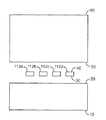
別々のフィルタ112a〜112dを実装するとき、フィルタと表面の間に任意の粒子、例えば埃があると、傾斜が生じ、ファイバに対する出射ビームまたは検出器に対する入射ビームの位置が変化する。400μmオーダの幅を有するフィルタを取り扱う場合、0.2μmの粒子であっても、1分以上の傾斜が生じ得る。
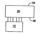
回折部品を用いて屈折させることができる。部品12a〜12dとして、(回折部品ではなく)屈折部品を用いると、システム全体の有効性が改善される。屈折部品12a〜12dを用いて、コリメートのみを行い、偏光させないとき、屈折レンズのSAGおよびレンズ間に要請されるピッチが低減され、より量産性の高い小型の光合波器を実現することができる。この実施形態の変形例において、屈折レンズ12a〜12dは、光ビームをコリメートするとともに部分的に偏光し、回折部品を用いてさらにビームを偏光する。これには好適な実施形態に対して有効性が改善されるという利点があり、ピッチは若干大きくなるが、屈折部品を用いて完全に偏光させる場合に比して、ピッチは小さくなる。回折部品を用いた場合、フィルタを固定する接着部材で回折部品を充填してもよい。したがって、所望の特性を得るために、接着部材の屈折率を考慮に入れて回折部品を設計してもよい。すなわち本発明の実施形態においては、傾斜を導入する機構は、基板15および基板55の上、およびこれらの間に配設される。
フィルタ112a〜112dと反射表面61との間に形成されるバウンスキャビティにおいて光を適当に反射させるために、ファイバ80は、サブアセンブリに対して所定の角度で傾斜している。その構成部品は、図5で示す光合波器の構成部品と同様のものである。ただし、検出器108a〜108dは大きい角度で受光するものなので、回折部品22a〜22dを必要としない。多重化回折部品68はファイバ80からの光をコリメートし、レンズアレイ14a〜14dは検出器108a〜108dにそれぞれ集光する。
Claims (23)
- 光アセンブリであって、
少なくとも2つの平行な表面を有するサブアセンブリと、
前記少なくとも2つの平行な表面のうちの一方の実装表面に隣接するフィルタと、
フィルタと実装表面の間にあって、フィルタの一部のみに当接するスタンドオフと、
スタンドオフおよびフィルタを固定する手段とを備えたことを特徴とする光アセンブリ。 - 請求項1に記載の光アセンブリであって、
スタンドオフは、所定位置に形成された少なくとも2つのスタンドオフを含み、フィルタに所定量の傾斜を与えるための高さを有することを特徴とする光アセンブリ。 - 光アセンブリであって、
実質的に平行な第1および第2の表面を有する第1の透明基板と、
実質的に平行な第3および第4の表面であって、第1および第2の表面と実質的に平行であるものを有する第2の透明基板と、
第2の透明基板上の反射部と、
第1の透明基板と反射部との間にあって、入射光ビームをフィルタ処理する複数のフィルタと、
複数のフィルタおよび反射部が第2の透明基板内でバウンスキャビティを構成し、
バウンスキャビティに入射される光ビームをコリメートするコリメートレンズと、
バウンスキャビティに入射される光ビームに傾斜を与える手段と、
光ビームを受ける入射ポートと、
光ビームを送る出射ポートとを備えたことを特徴とする光アセンブリ。 - 請求項3に記載の光アセンブリであって、
入射ポートおよび出射ポートの一方が第4の表面上の透明部分であることを特徴とする光アセンブリ。 - 請求項3に記載の光アセンブリであって、
傾斜を与える手段は、第1および第2の基板の間にあることを特徴とする光アセンブリ。 - 請求項5に記載の光アセンブリであって、
傾斜を与える手段は、複数のリソグラフ部品を有することを特徴とする光アセンブリ。 - 請求項5に記載の光アセンブリであって、
傾斜を与える手段は、複数のプリズムを有することを特徴とする光アセンブリ。 - 請求項3に記載の光アセンブリであって、
複数のフィルタが固定された表面の上にある回折レンズをさらに有することを特徴とする光アセンブリ。 - 請求項8に記載の光アセンブリであって、
回折レンズを充填し、複数のフィルタを固定する接着材料をさらに有することを特徴とする光アセンブリ。 - 請求項3に記載の光アセンブリであって、
傾斜を与える手段は、入射ポートおよび複数のフィルタの間にあることを特徴とする光アセンブリ。 - 請求項3に記載の光アセンブリであって、
第4の表面は平坦であることを特徴とする光アセンブリ。 - 請求項10に記載の光アセンブリであって、
入射ポートおよび出射ポートは第1の表面上にあることを特徴とする光アセンブリ。 - 光アセンブリであって、
第1および第2の表面を有する第1の透明基板と、
実質的に平行な第3および第4の表面を有する第2の透明基板と、
第2の透明基板上にあって、第2の透明基板内にバウンスキャビティを構成する反射部と、
第1の透明基板と反射部との間にあって、入射光ビームをフィルタ処理する複数のフィルタと、
複数のフィルタおよび反射部が第2の透明基板内でバウンスキャビティを構成し、
第1および第2の基板の一方の上にある光ビームを受ける入射ポートと、
第1および第2の基板の一方の上にある光ビームを送る出射ポートと、
第1および第2の基板の間にあるバウンスキャビティに入射される光ビームに傾斜を与える手段とを備えたことを特徴とする光アセンブリ。 - 請求項13に記載の光アセンブリであって、
傾斜を与える手段は、複数のプリズムを有することを特徴とする光アセンブリ。 - 請求項13に記載の光アセンブリであって、
傾斜を与える手段は、複数の回折部品を有することを特徴とする光アセンブリ。 - 請求項13に記載の光アセンブリであって、
傾斜を与える手段は、傾斜した表面であることを特徴とする光アセンブリ。 - 光アセンブリを作製する方法であって、
第1および第2の表面を有する第1の透明基板を提供するステップと、
実質的に平行な第3および第4の表面を有する第2の透明基板を提供するステップと、
第2の透明基板の第4の表面上に反射部を設けて、第2の透明基板内にバウンスキャビティを形成するステップと、
第1の透明基板とバウンスキャビティとの間に複数のフィルタを設けるステップと、
第1の透明基板、第2の透明基板、および複数のフィルタのうち少なくとも2つを一体にダイボンディングするステップとを有することを特徴とする方法。 - 請求項17に記載の方法であって、
複数のフィルタを第2の透明基板にダイボンディングした後、第2の透明基板を複数のフィルタにダイボンディングするステップをさらに有することを特徴とする方法。 - 請求項17に記載の方法であって、
ダイ実装部上に第4の表面を固定して、複数のフィルタを第3の表面に接合させるステップをさらに有することを特徴とする方法。 - 請求項19に記載の方法であって、
接合させるステップの前に、複数のフィルタを第3の表面上に実装するためのスタンドオフを設けるステップをさらに有することを特徴とする方法。 - 請求項20に記載の方法であって、
スタンドオフを設けるステップは、リソグラフ技術を用いて部品を形成するステップを有することを特徴とする方法。 - 請求項20に記載の方法であって、
スタンドオフ上を含めて、第3の表面に接着材料を供給するステップを有することを特徴とする方法。 - 請求項22に記載の方法であって、
接合させるステップは、フィルタを室温の接着材料に当接させて、第2の基板を加熱するステップを有することを特徴とする方法。
Applications Claiming Priority (4)
| Application Number | Priority Date | Filing Date | Title |
|---|---|---|---|
| US70150505P | 2005-07-22 | 2005-07-22 | |
| US60/701,505 | 2005-07-22 | ||
| US11/295,720 US7466502B2 (en) | 2005-12-07 | 2005-12-07 | Optical wavelength division coupler and associated methods |
| US11/295,720 | 2005-12-07 |
Related Parent Applications (1)
| Application Number | Title | Priority Date | Filing Date |
|---|---|---|---|
| JP2008523033A Division JP5568236B2 (ja) | 2005-07-22 | 2006-07-24 | 光波長分割カプラおよび関連方法 |
Publications (2)
| Publication Number | Publication Date |
|---|---|
| JP2013178529A true JP2013178529A (ja) | 2013-09-09 |
| JP5852040B2 JP5852040B2 (ja) | 2016-02-03 |
Family
ID=37683863
Family Applications (2)
| Application Number | Title | Priority Date | Filing Date |
|---|---|---|---|
| JP2008523033A Expired - Fee Related JP5568236B2 (ja) | 2005-07-22 | 2006-07-24 | 光波長分割カプラおよび関連方法 |
| JP2013077081A Expired - Fee Related JP5852040B2 (ja) | 2005-07-22 | 2013-04-02 | 光学的アセンブリ |
Family Applications Before (1)
| Application Number | Title | Priority Date | Filing Date |
|---|---|---|---|
| JP2008523033A Expired - Fee Related JP5568236B2 (ja) | 2005-07-22 | 2006-07-24 | 光波長分割カプラおよび関連方法 |
Country Status (5)
| Country | Link |
|---|---|
| US (2) | US7817883B2 (ja) |
| EP (1) | EP1910880B1 (ja) |
| JP (2) | JP5568236B2 (ja) |
| CA (1) | CA2616311C (ja) |
| WO (1) | WO2007014125A2 (ja) |
Families Citing this family (23)
| Publication number | Priority date | Publication date | Assignee | Title |
|---|---|---|---|---|
| US7887243B2 (en) | 2007-03-16 | 2011-02-15 | Honeywell Federal Manufacturing & Technologies, Llc | Miniature mechanical transfer optical coupler |
| KR20090011518A (ko) * | 2007-07-26 | 2009-02-02 | 엘지전자 주식회사 | 영상표시기기 및 영상표시방법 |
| KR101103738B1 (ko) * | 2010-05-28 | 2012-01-11 | 엘지이노텍 주식회사 | Sag보정이 가능한 MEMS액추에이터 장착형 카메라 모듈 및 이를 이용한 Sag보정 방법 |
| CN103201969B (zh) * | 2010-10-08 | 2016-10-19 | 慧与发展有限责任合伙企业 | 使用激光器阵列的光复用 |
| CN102684794A (zh) * | 2012-06-06 | 2012-09-19 | 苏州旭创科技有限公司 | 应用于高速并行长距离传输的新型波分复用解复用光组件 |
| CN102890313B (zh) * | 2012-10-22 | 2015-07-15 | 索尔思光电(成都)有限公司 | Cwdm多工/解多工器系统及其制造方法 |
| CN203732758U (zh) * | 2014-03-17 | 2014-07-23 | 苏州旭创科技有限公司 | 波分复用解复用装置 |
| JP2015225979A (ja) * | 2014-05-28 | 2015-12-14 | 日立金属株式会社 | 光通信モジュール |
| US9419718B2 (en) * | 2014-08-18 | 2016-08-16 | Cisco Technology, Inc. | Aligning optical components in a multichannel receiver or transmitter platform |
| US10459174B2 (en) | 2014-12-19 | 2019-10-29 | Hewlett Packard Enterprise Development Lp | Bonded filter substrates |
| JP6449429B2 (ja) * | 2015-03-05 | 2019-01-09 | 三菱電機株式会社 | 光合波器の製造方法 |
| US10281651B2 (en) | 2015-04-10 | 2019-05-07 | Hewlett Packard Enterprise Development Lp | Optical zig-zags |
| US9692522B2 (en) * | 2015-04-15 | 2017-06-27 | Cisco Technology, Inc. | Multi-channel optical receiver or transmitter with a ball lens |
| TWI581027B (zh) * | 2015-07-17 | 2017-05-01 | 信泰光學(深圳)有限公司 | 光學裝置 |
| KR102064793B1 (ko) * | 2015-12-18 | 2020-01-10 | 한국전자통신연구원 | 광다중화기 또는 광역다중화기를 위한 다채널 박막 필터 접합 방법 |
| US20180017735A1 (en) * | 2016-07-13 | 2018-01-18 | Futurewei Technologies, Inc. | Wavelength Division Multiplexer/Demultiplexer with Flexibility of Optical Adjustment |
| WO2018117278A1 (ko) * | 2016-12-19 | 2018-06-28 | 엠피닉스 주식회사 | 광학 디먹스 블록 및 광학 먹스 블록 |
| WO2019126521A1 (en) | 2017-12-21 | 2019-06-27 | Corning Incorporated | Multi-layer insulated glass unit comprising a low cte glass layer |
| US11360266B2 (en) | 2018-02-09 | 2022-06-14 | Mitsubishi Electric Corporation | Method for manufacturing optical multiplexer/demultiplexer |
| WO2019204043A1 (en) * | 2018-04-17 | 2019-10-24 | Alliance Fiber Optic Products, Inc. | Multi-layer wavelength-division multiplexing devices |
| WO2019207438A1 (en) * | 2018-04-26 | 2019-10-31 | SM Optics S.r.l. | Optical device for demultiplexing and multiplexing modes with different orbital angular momentum |
| WO2020028077A1 (en) | 2018-07-31 | 2020-02-06 | Alliance Fiber Optic Products, Inc. | Wavelength-division multiplexing devices with modified angles of incidence |
| US20240369772A1 (en) * | 2023-05-01 | 2024-11-07 | Cisco Technology, Inc. | Wavelength multiplexing or demultiplexing using a lens array with an angled facet |
Citations (3)
| Publication number | Priority date | Publication date | Assignee | Title |
|---|---|---|---|---|
| JP2002010118A (ja) * | 2000-06-22 | 2002-01-11 | Shinten Sangyo Co Ltd | 固体撮像装置 |
| US6563976B1 (en) * | 2000-05-09 | 2003-05-13 | Blaze Network Products, Inc. | Cost-effective wavelength division multiplexer and demultiplexer |
| JP2003270406A (ja) * | 2002-03-15 | 2003-09-25 | Ricoh Opt Ind Co Ltd | 光モジュールおよび光結合方法 |
Family Cites Families (28)
| Publication number | Priority date | Publication date | Assignee | Title |
|---|---|---|---|---|
| IT1109751B (it) | 1978-01-31 | 1985-12-23 | Nippon Telegraph & Telephone | Moltiplatore e demultiplatore ottico |
| JPS54103055A (en) * | 1978-01-31 | 1979-08-14 | Nippon Telegr & Teleph Corp <Ntt> | Spectrometer |
| NL8104123A (nl) * | 1981-09-07 | 1983-04-05 | Philips Nv | Optische multiplex- en demultiplexinrichting. |
| FR2539518A1 (fr) | 1983-01-18 | 1984-07-20 | Comp Generale Electricite | Separateur optique en longueurs d'ondes, notamment pour systeme de transmission multiplex a fibres optiques |
| JPS59200210A (ja) * | 1983-04-28 | 1984-11-13 | Toshiba Corp | 光分波器 |
| US5074646A (en) | 1989-04-28 | 1991-12-24 | At&T Bell Laboratories | Planar reflective optical devices |
| US5734156A (en) * | 1994-12-22 | 1998-03-31 | Santa Barbara Research Center | Optical device assembly and its preparation using metallic bump bonding and a stand-off for bonding together two planar optical components |
| US5526338A (en) * | 1995-03-10 | 1996-06-11 | Yeda Research & Development Co. Ltd. | Method and apparatus for storage and retrieval with multilayer optical disks |
| US6096155A (en) | 1996-09-27 | 2000-08-01 | Digital Optics Corporation | Method of dicing wafer level integrated multiple optical elements |
| US5835517A (en) * | 1996-10-04 | 1998-11-10 | W. L. Gore & Associates, Inc. | WDM multiplexer-demultiplexer using Fabry-Perot filter array |
| US5963684A (en) * | 1997-02-13 | 1999-10-05 | Lucent Technologies Inc. | Multiple-wavelength optical transceiver |
| US5859717A (en) * | 1997-02-14 | 1999-01-12 | Corning Oca Corporation | Multiplexing device with precision optical block |
| US6024453A (en) * | 1997-04-29 | 2000-02-15 | Balzers Aktiengesellshaft | Method of rapidly producing color changes in an optical light path |
| US5894535A (en) * | 1997-05-07 | 1999-04-13 | Hewlett-Packard Company | Optical waveguide device for wavelength demultiplexing and waveguide crossing |
| US6243513B1 (en) | 1997-12-13 | 2001-06-05 | Lightchip, Inc. | Wavelength division multiplexing/demultiplexing devices using diffractive optic lenses |
| US6198864B1 (en) * | 1998-11-24 | 2001-03-06 | Agilent Technologies, Inc. | Optical wavelength demultiplexer |
| US6384978B1 (en) * | 1999-03-19 | 2002-05-07 | Qtera Corporation | Temperature-compensated optical filter assemblies and related methods |
| WO2001014924A1 (en) | 1999-08-26 | 2001-03-01 | The Ohio State University | Device for producing optically-controlled incremental time delays |
| US6198432B1 (en) * | 1999-09-29 | 2001-03-06 | Trimble Navigation Limited | Method and apparatus for automatic and autonomous assignment of PRN codes to a multiplicity of pseudolites |
| US6684010B1 (en) | 2000-03-03 | 2004-01-27 | Digital Optics Corp. | Wavelength compensated optical wavelength division coupler and associated methods |
| US6941072B2 (en) * | 2000-10-17 | 2005-09-06 | Jds Uniphase Corporation | Compact optical multiplexer/demultiplexer |
| US6404958B1 (en) * | 2000-10-31 | 2002-06-11 | Digital Optics Corp. | Intergrated optical coupler |
| JP3784701B2 (ja) * | 2001-11-20 | 2006-06-14 | 株式会社日立製作所 | 光回路部材および光トランシーバ |
| JP2004206057A (ja) * | 2002-11-01 | 2004-07-22 | Omron Corp | 光合分波器及び光合分波器の製造方法 |
| US6947229B2 (en) * | 2003-12-19 | 2005-09-20 | Intel Corporation | Etalon positioning using solder balls |
| JP2005274700A (ja) * | 2004-03-23 | 2005-10-06 | Nippon Telegr & Teleph Corp <Ntt> | 光合分波器 |
| US7349602B2 (en) * | 2004-10-08 | 2008-03-25 | Agilent Technologies, Inc. | Wavelength division multiplexer architecture |
| US7546780B2 (en) * | 2005-09-30 | 2009-06-16 | Rockwell Automation Technologies, Inc. | Sensor mounting structure allowing for adjustment of sensor position |
-
2006
- 2006-07-24 EP EP06788267.0A patent/EP1910880B1/en not_active Not-in-force
- 2006-07-24 CA CA2616311A patent/CA2616311C/en not_active Expired - Fee Related
- 2006-07-24 JP JP2008523033A patent/JP5568236B2/ja not_active Expired - Fee Related
- 2006-07-24 WO PCT/US2006/028610 patent/WO2007014125A2/en not_active Ceased
-
2008
- 2008-11-17 US US12/292,313 patent/US7817883B2/en not_active Expired - Fee Related
-
2010
- 2010-10-18 US US12/906,581 patent/US8532445B2/en not_active Expired - Fee Related
-
2013
- 2013-04-02 JP JP2013077081A patent/JP5852040B2/ja not_active Expired - Fee Related
Patent Citations (3)
| Publication number | Priority date | Publication date | Assignee | Title |
|---|---|---|---|---|
| US6563976B1 (en) * | 2000-05-09 | 2003-05-13 | Blaze Network Products, Inc. | Cost-effective wavelength division multiplexer and demultiplexer |
| JP2002010118A (ja) * | 2000-06-22 | 2002-01-11 | Shinten Sangyo Co Ltd | 固体撮像装置 |
| JP2003270406A (ja) * | 2002-03-15 | 2003-09-25 | Ricoh Opt Ind Co Ltd | 光モジュールおよび光結合方法 |
Also Published As
| Publication number | Publication date |
|---|---|
| US20090103866A1 (en) | 2009-04-23 |
| CA2616311A1 (en) | 2007-02-01 |
| WO2007014125A3 (en) | 2007-11-15 |
| JP5852040B2 (ja) | 2016-02-03 |
| EP1910880A4 (en) | 2010-02-03 |
| EP1910880A2 (en) | 2008-04-16 |
| JP2009503567A (ja) | 2009-01-29 |
| US8532445B2 (en) | 2013-09-10 |
| US20110033152A1 (en) | 2011-02-10 |
| JP5568236B2 (ja) | 2014-08-06 |
| US7817883B2 (en) | 2010-10-19 |
| CA2616311C (en) | 2014-09-30 |
| EP1910880B1 (en) | 2016-03-30 |
| WO2007014125A2 (en) | 2007-02-01 |
Similar Documents
| Publication | Publication Date | Title |
|---|---|---|
| JP5852040B2 (ja) | 光学的アセンブリ | |
| KR100889976B1 (ko) | 광 모듈과 이를 이용한 광 센서 및 그 제조방법 | |
| US6563976B1 (en) | Cost-effective wavelength division multiplexer and demultiplexer | |
| US7076125B2 (en) | Optical circuit element and production method therefor, array-form optical circuit element, optical circuit device using it | |
| US11675146B2 (en) | Optical assembly and manufacturing method thereof | |
| US8742320B2 (en) | Spectral module and method for manufacturing spectral module | |
| JP5528632B2 (ja) | 波長分割多重化又は波長分割逆多重化の装置 | |
| CN210605074U (zh) | 一种光学组件 | |
| US20020076480A1 (en) | Low cost step tunable light source | |
| US20070297719A1 (en) | Integrated Microlens Reflector And Light Coupler | |
| US20200379182A1 (en) | Precision tff posa and wdm systems using parallel fiber interface devices | |
| US7466502B2 (en) | Optical wavelength division coupler and associated methods | |
| CN108627924B (zh) | 用于监测光收发器中的光输出功率的两部分光耦合子组件 | |
| JP2003248142A (ja) | 二次元光学部材アレイ及び二次元導波路装置 | |
| CN105229508A (zh) | 用于形成可连接至光纤的光电模块的方法和可连接到至少一个光纤的光电模块 | |
| US12481115B2 (en) | Optical device and optical component | |
| JP3910846B2 (ja) | 二次元光学部材アレイ及び二次元導波路装置並びにそれらの製造方法 | |
| US8447151B2 (en) | Triplexer for an optical fiber, package including the same, and associated methods | |
| JP2005274700A (ja) | 光合分波器 | |
| JPH1090565A (ja) | 光学素子及びその製造方法 | |
| JPH08220357A (ja) | 光学接続装置およびその製造方法 | |
| JP2924872B2 (ja) | 光ヘッドとその組立方法 | |
| KR20130016456A (ko) | 어레이 광 콜리메이터 | |
| KR20120086588A (ko) | 어레이 광 콜리메이터 | |
| CN111580225A (zh) | 光模块的安装构造体 |
Legal Events
| Date | Code | Title | Description |
|---|---|---|---|
| A977 | Report on retrieval |
Free format text: JAPANESE INTERMEDIATE CODE: A971007 Effective date: 20140227 |
|
| A131 | Notification of reasons for refusal |
Free format text: JAPANESE INTERMEDIATE CODE: A131 Effective date: 20140603 |
|
| A521 | Request for written amendment filed |
Free format text: JAPANESE INTERMEDIATE CODE: A523 Effective date: 20140903 |
|
| A711 | Notification of change in applicant |
Free format text: JAPANESE INTERMEDIATE CODE: A711 Effective date: 20140903 |
|
| A131 | Notification of reasons for refusal |
Free format text: JAPANESE INTERMEDIATE CODE: A131 Effective date: 20150303 |
|
| A521 | Request for written amendment filed |
Free format text: JAPANESE INTERMEDIATE CODE: A523 Effective date: 20150513 |
|
| A711 | Notification of change in applicant |
Free format text: JAPANESE INTERMEDIATE CODE: A711 Effective date: 20150513 |
|
| A521 | Request for written amendment filed |
Free format text: JAPANESE INTERMEDIATE CODE: A523 Effective date: 20150616 |
|
| TRDD | Decision of grant or rejection written | ||
| A01 | Written decision to grant a patent or to grant a registration (utility model) |
Free format text: JAPANESE INTERMEDIATE CODE: A01 Effective date: 20151104 |
|
| A61 | First payment of annual fees (during grant procedure) |
Free format text: JAPANESE INTERMEDIATE CODE: A61 Effective date: 20151203 |
|
| R150 | Certificate of patent or registration of utility model |
Ref document number: 5852040 Country of ref document: JP Free format text: JAPANESE INTERMEDIATE CODE: R150 |
|
| R250 | Receipt of annual fees |
Free format text: JAPANESE INTERMEDIATE CODE: R250 |
|
| S111 | Request for change of ownership or part of ownership |
Free format text: JAPANESE INTERMEDIATE CODE: R313111 |
|
| R350 | Written notification of registration of transfer |
Free format text: JAPANESE INTERMEDIATE CODE: R350 |
|
| R250 | Receipt of annual fees |
Free format text: JAPANESE INTERMEDIATE CODE: R250 |
|
| S111 | Request for change of ownership or part of ownership |
Free format text: JAPANESE INTERMEDIATE CODE: R313113 |
|
| R350 | Written notification of registration of transfer |
Free format text: JAPANESE INTERMEDIATE CODE: R350 |
|
| R250 | Receipt of annual fees |
Free format text: JAPANESE INTERMEDIATE CODE: R250 |
|
| R250 | Receipt of annual fees |
Free format text: JAPANESE INTERMEDIATE CODE: R250 |
|
| LAPS | Cancellation because of no payment of annual fees | ||
| S111 | Request for change of ownership or part of ownership |
Free format text: JAPANESE INTERMEDIATE CODE: R313111 |
|
| R350 | Written notification of registration of transfer |
Free format text: JAPANESE INTERMEDIATE CODE: R350 |