JP2014013893A - トンネル電界効果トランジスタデバイスおよびそのデバイスの製造方法 - Google Patents
トンネル電界効果トランジスタデバイスおよびそのデバイスの製造方法 Download PDFInfo
- Publication number
- JP2014013893A JP2014013893A JP2013121057A JP2013121057A JP2014013893A JP 2014013893 A JP2014013893 A JP 2014013893A JP 2013121057 A JP2013121057 A JP 2013121057A JP 2013121057 A JP2013121057 A JP 2013121057A JP 2014013893 A JP2014013893 A JP 2014013893A
- Authority
- JP
- Japan
- Prior art keywords
- layer
- tfet
- source
- drain
- Prior art date
- Legal status (The legal status is an assumption and is not a legal conclusion. Google has not performed a legal analysis and makes no representation as to the accuracy of the status listed.)
- Granted
Links
Images





Classifications
-
- H—ELECTRICITY
- H10—SEMICONDUCTOR DEVICES; ELECTRIC SOLID-STATE DEVICES NOT OTHERWISE PROVIDED FOR
- H10D—INORGANIC ELECTRIC SEMICONDUCTOR DEVICES
- H10D48/00—Individual devices not covered by groups H10D1/00 - H10D44/00
- H10D48/383—Quantum effect devices, e.g. of devices using quantum reflection, diffraction or interference effects
-
- H—ELECTRICITY
- H10—SEMICONDUCTOR DEVICES; ELECTRIC SOLID-STATE DEVICES NOT OTHERWISE PROVIDED FOR
- H10D—INORGANIC ELECTRIC SEMICONDUCTOR DEVICES
- H10D12/00—Bipolar devices controlled by the field effect, e.g. insulated-gate bipolar transistors [IGBT]
- H10D12/211—Gated diodes
-
- H—ELECTRICITY
- H10—SEMICONDUCTOR DEVICES; ELECTRIC SOLID-STATE DEVICES NOT OTHERWISE PROVIDED FOR
- H10D—INORGANIC ELECTRIC SEMICONDUCTOR DEVICES
- H10D30/00—Field-effect transistors [FET]
- H10D30/01—Manufacture or treatment
- H10D30/021—Manufacture or treatment of FETs having insulated gates [IGFET]
Landscapes
- Insulated Gate Type Field-Effect Transistor (AREA)
- Thin Film Transistor (AREA)
Abstract
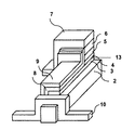
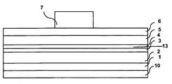
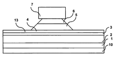
【解決手段】少なくとも以下の層、高ドープされたドレイン層6、高ドープされたソース層2、チャネル層5、ソース層2に沿って延びるゲート誘電体層8とゲート電極層9、およびゲート誘電体層8とソース層2との間にこれらに沿って延びる高ドープポケット層3、を含み、ポケット層3はソース層2およびチャネル層5の間まで、これらに沿って延びている。
【選択図】図1
Description
ドレイン半導体材料からなる、高くnドープされたドレイン層、
ドレイン層に対して反対にドープされ、高くpドープされた、ソース半導体材料からなるソース層、および
ゲート誘電体層とゲート電極層を含むゲート構造、
からなるトンネル電界効果トランジスタデバイス(TFET)について記載される。
ドレイン半導体材料からなる高くpドープされたドレイン層、
ソース半導体材料からなる高くnドープしたソース層、
ゲート誘電体層とゲート電極層を含むゲート構造、
ソース層に対してカウンタードープされ、ソース層とゲート構造のゲート誘電体層との間にこれらに沿って延びるポケット層、
ソースとドレイン層の間に配置されたチャネル半導体材料からなる低ドープチャネル層、を含む。
例えば1016cm−3と5×1020cm−3の間、好適には1017cm−3と1020cm−3の間のような、1016cm−3以上のドーピングレベルを有する、ドレイン半導体材料からなる高ドープされたドレイン層6。
例えば1016cm−3と5×1020cm−3の間、好適には5×1018cm−3と1020cm−3の間のような、1016cm−3以上のドーピングレベルを有する、ドレイン層に対して反対にドープされた、ソース半導体材料からなる高ドープされたソース層2。
例えば0cm−3と1018cm−3の間、好適には1015cm−3と1017cm−3の間のような1018cm−3より低いドーピングレベルの低ドープまたはアンドープのチャネル半導体材料からなるチャネル層5。チャネル層5は、ソース2とドレイン層6との間に配置される。
ゲート誘電体層8とゲート電極層9とを含むゲート構造8、9。ゲート誘電体層8は、ソース層2に沿って延び、ゲート電極層9は、ソース層2に面するゲート誘電体層8の面と反対のゲート誘電体層8の面に沿ったゲート誘電体層に沿って延びる。ゲート電極層9は、ゲート誘電体層8を超えて延びない。ゲート電極層9とゲート誘電体層8の少なくとも一部は、チャネル層5の少なくとも一部に沿って延びても良い。
ゲート誘電体層8とソース層2との間にこれらに沿って延びる、高ドープのポケット層3。ポケット層3は、例えば1016cm−3と5×1020cm−3の間、好適には1017cm−3と1020cm−3の間のような、1016cm−3以上のドーピングレベルを有する半導体材料からなる。
更に、本発明では重要ではないが、基板層とソースコンタクト電極10が提供される。
加えて、ドレインコンタクト電極7が示され、これはドレイン層6の上に提供される。
Claims (16)
- トンネル電界効果トランジスタデバイス(TFET)であって、少なくとも以下の層:
例えば1016cm−3と5×1020cm−3の間、好適には1017cm−3と1020cm−3の間のような、1016cm−3以上のドーピングレベルを有する、ドレイン半導体材料からなる高ドープされたドレイン層(6)、
例えば1016cm−3と5×1020cm−3の間、好適には5×1018cm−3と1020cm−3の間のような、1016cm−3以上のドーピングレベルを有する、ドレイン層に対して反対にドープされた、ソース半導体材料からなる高ドープされたソース層(2)、
例えば0cm−3と1018cm−3の間、好適には1015cm−3と1017cm−3の間のような1018cm−3より低いドーピングレベルの低ドープの、またはアンドープのチャネル半導体材料からなり、ソース(2)とドレイン層(6)との間に配置されるチャネル層(5)、
ゲート誘電体層(8)とゲート電極層(9)とを含むゲート構造(8、9)であって、ゲート誘電体層(8)はソース層(2)に沿って延び、ゲート電極層(9)はソース層(2)に面するゲート誘電体層(8)の面と反対のゲート誘電体層(8)の面に沿ったゲート誘電体層に沿って延び、ゲート誘電体層(8)を超えて延びないゲート構造(8、9)、
例えば1016cm−3と5×1020cm−3の間、好適には1017cm−3と1020cm−3の間のような、1016cm−3以上のドーピングレベルを有する半導体材料からなり、ゲート誘電体層(8)とソース層(2)との間にこれらに沿って延びる、高ドープのポケット層(3)、
から形成され、
ポケット層(3)は、ソース層(2)とチャネル層(5)との間にこれらに沿って延びることを特徴とするTFET。 - ポケット層(3)は、ソース層(2)に対してカウンタードープされた請求項1に記載のTFET。
- 少なくともゲート誘電体層(8)の一部は、少なくともチャネル層(5)の一部に沿って延びて、チャネル層(5)と接続する請求項1または2に記載のTFET。
- ソース層(2)、ポケット層(3)、チャネル層(5)、およびドレイン層(6)は、実質的に平坦で、互いに上部に沿うように配置される請求項1〜3のいずれかに記載のTFET。
- TFETは、3次元Fin−FET状の構造(Fin−TFET)を有し、フィン状の構造はソース層(2)を形成する請求項1〜3のいずれかに記載のTFET。
- TFETは、垂直ナノ構造(ナノワイヤ)である請求項1〜3のいずれかに記載のTFET。
- ドレイン層(6)はドレインコンタクト電極(7)と接続し、および/またはソース(2)はソースコンタクト電極(10)と電気的に接続し、および/またはゲート電極(9)は、ゲートコンタクト電極(11)と電気的に接続する、請求項1〜6のいずれかに記載のTFET。
- エッチストップ層(4)は、チャネル層(5)とポケット層(3)との間にこれらに沿って存在し、エッチストップ層は、例えば1016cm−3と5×1020cm−3の間、好適には1017cm−3と1020cm−3の間のような、1016cm−3以上のドーピングレベルを有する半導体材料から形成される請求項1〜7のいずれかに記載のTFET。
- リークストップ層(13)は、チャネル層(5)とポケット層(3)との間に、これらに沿って存在し、リークストップ層は、例えば1016cm−3と5×1020cm−3の間、好適には1017cm−3と1020cm−3の間のような、1016cm−3以上のドーピングレベルを有する半導体材料から形成される請求項1〜8のいずれかに記載のTFET。
- 請求項1〜9のいずれかにかかるTFETの製造方法。
- ソース層(2)、ポケット層(3)、チャネル層(5)、およびドレイン層(6)を含む層スタックが形成され、その後にドレイン層(6)とチャネル層(5)の一部がポケット層(3)まで除去され、その後にゲート誘電体層(8)が層スタックの露出した表面に適用され、その後にゲート電極層(9)がゲート誘電体層(8)に適用される請求項10に記載のTFETの製造方法。
- エッチストップ層(4)までの少なくとも部分的なエッチングにより、ドレイン層(6)とチャネル層(5)の一部がポケット層(3)まで除去される請求項11に記載のTFETの製造方法。
- エッチストップ層(4)はポケット層(3)である請求項12に記載のTFETの製造方法。
- リークストップ層(13)は、ポケット層(3)とチャネル層(5)との間に提供され、ソース(2)からドレイン(6)に層スタックのバルクを通って流れる電流を防止する請求項13に記載のTFETの製造方法。
- エッチストップ層(4)はポケット層(3)とは異なり、ドレイン層(6)とチャネル層(5)の一部をエッチング除去した後に除去される、少なくとも請求項8と組み合わせた請求項12に記載のTFETの製造方法。
- ドレインコンタクト電極(7)は、ドレイン層(6)の上に形成される請求項10〜15のいずれかに記載のTFETの製造方法。
Applications Claiming Priority (2)
| Application Number | Priority Date | Filing Date | Title |
|---|---|---|---|
| EP12172186.4A EP2674978B1 (en) | 2012-06-15 | 2012-06-15 | Tunnel field effect transistor device and method for making the device |
| EP12172186.4 | 2012-06-15 |
Publications (2)
| Publication Number | Publication Date |
|---|---|
| JP2014013893A true JP2014013893A (ja) | 2014-01-23 |
| JP6178631B2 JP6178631B2 (ja) | 2017-08-09 |
Family
ID=46456348
Family Applications (1)
| Application Number | Title | Priority Date | Filing Date |
|---|---|---|---|
| JP2013121057A Active JP6178631B2 (ja) | 2012-06-15 | 2013-06-07 | トンネル電界効果トランジスタデバイスおよびそのデバイスの製造方法 |
Country Status (3)
| Country | Link |
|---|---|
| US (1) | US9070720B2 (ja) |
| EP (1) | EP2674978B1 (ja) |
| JP (1) | JP6178631B2 (ja) |
Families Citing this family (8)
| Publication number | Priority date | Publication date | Assignee | Title |
|---|---|---|---|---|
| US9583590B2 (en) | 2013-09-27 | 2017-02-28 | Samsung Electronics Co., Ltd. | Integrated circuit devices including FinFETs and methods of forming the same |
| US9786769B2 (en) | 2013-12-26 | 2017-10-10 | Intel Corporation | Complementary tunneling FET devices and method for forming the same |
| KR20150085663A (ko) * | 2014-01-16 | 2015-07-24 | 삼성전자주식회사 | 터널링 전계 효과 트랜지스터 |
| US9419114B2 (en) * | 2014-01-17 | 2016-08-16 | Imec Vzw | Tunnel field-effect transistor |
| US9741811B2 (en) | 2014-12-15 | 2017-08-22 | Samsung Electronics Co., Ltd. | Integrated circuit devices including source/drain extension regions and methods of forming the same |
| US9362383B1 (en) * | 2015-09-17 | 2016-06-07 | International Business Machines Corporation | Highly scaled tunnel FET with tight pitch and method to fabricate same |
| US9508597B1 (en) | 2015-09-18 | 2016-11-29 | Globalfoundries Inc. | 3D fin tunneling field effect transistor |
| US11164939B2 (en) * | 2018-06-27 | 2021-11-02 | Taiwan Semiconductor Manufacturing Co., Ltd. | Tunnel field-effect transistor and method for forming the same |
Citations (6)
| Publication number | Priority date | Publication date | Assignee | Title |
|---|---|---|---|---|
| JPS5775464A (en) * | 1980-10-28 | 1982-05-12 | Semiconductor Res Found | Semiconductor device controlled by tunnel injection |
| JPS57186374A (en) * | 1981-05-12 | 1982-11-16 | Semiconductor Res Found | Tunnel injection type travelling time effect semiconductor device |
| JPS6399580A (ja) * | 1987-10-01 | 1988-04-30 | Semiconductor Res Found | トンネル注入制御半導体デバイス |
| JPH04277680A (ja) * | 1991-03-05 | 1992-10-02 | Nec Corp | トンネルトランジスタ及びその製造方法 |
| JP2009532905A (ja) * | 2006-04-04 | 2009-09-10 | マイクロン テクノロジー, インク. | ナノFinトンネリング・トランジスタ |
| US20120043607A1 (en) * | 2010-08-18 | 2012-02-23 | Mathieu Luisier | Tunneling Field-Effect Transistor with Low Leakage Current |
Family Cites Families (6)
| Publication number | Priority date | Publication date | Assignee | Title |
|---|---|---|---|---|
| JP2773487B2 (ja) * | 1991-10-15 | 1998-07-09 | 日本電気株式会社 | トンネルトランジスタ |
| US6756633B2 (en) * | 2001-12-27 | 2004-06-29 | Silicon Storage Technology, Inc. | Semiconductor memory array of floating gate memory cells with horizontally oriented floating gate edges |
| US7659570B2 (en) * | 2005-05-09 | 2010-02-09 | Alpha & Omega Semiconductor Ltd. | Power MOSFET device structure for high frequency applications |
| US8692324B2 (en) * | 2005-07-13 | 2014-04-08 | Ciclon Semiconductor Device Corp. | Semiconductor devices having charge balanced structure |
| US7439135B2 (en) * | 2006-04-04 | 2008-10-21 | International Business Machines Corporation | Self-aligned body contact for a semiconductor-on-insulator trench device and method of fabricating same |
| EP1883116B1 (en) * | 2006-07-26 | 2020-03-11 | Semiconductor Components Industries, LLC | Semiconductor device with high breakdown voltage and manufacturing method thereof |
-
2012
- 2012-06-15 EP EP12172186.4A patent/EP2674978B1/en active Active
-
2013
- 2013-05-29 US US13/904,303 patent/US9070720B2/en active Active
- 2013-06-07 JP JP2013121057A patent/JP6178631B2/ja active Active
Patent Citations (6)
| Publication number | Priority date | Publication date | Assignee | Title |
|---|---|---|---|---|
| JPS5775464A (en) * | 1980-10-28 | 1982-05-12 | Semiconductor Res Found | Semiconductor device controlled by tunnel injection |
| JPS57186374A (en) * | 1981-05-12 | 1982-11-16 | Semiconductor Res Found | Tunnel injection type travelling time effect semiconductor device |
| JPS6399580A (ja) * | 1987-10-01 | 1988-04-30 | Semiconductor Res Found | トンネル注入制御半導体デバイス |
| JPH04277680A (ja) * | 1991-03-05 | 1992-10-02 | Nec Corp | トンネルトランジスタ及びその製造方法 |
| JP2009532905A (ja) * | 2006-04-04 | 2009-09-10 | マイクロン テクノロジー, インク. | ナノFinトンネリング・トランジスタ |
| US20120043607A1 (en) * | 2010-08-18 | 2012-02-23 | Mathieu Luisier | Tunneling Field-Effect Transistor with Low Leakage Current |
Also Published As
| Publication number | Publication date |
|---|---|
| US9070720B2 (en) | 2015-06-30 |
| US20130334500A1 (en) | 2013-12-19 |
| EP2674978A1 (en) | 2013-12-18 |
| EP2674978B1 (en) | 2020-07-29 |
| JP6178631B2 (ja) | 2017-08-09 |
Similar Documents
| Publication | Publication Date | Title |
|---|---|---|
| JP6178631B2 (ja) | トンネル電界効果トランジスタデバイスおよびそのデバイスの製造方法 | |
| US8653504B2 (en) | Complementary tunneling field effect transistor and method for forming the same | |
| US9136363B2 (en) | Compound tunneling field effect transistor integrated on silicon substrate and method for fabricating the same | |
| KR101307191B1 (ko) | 터널 전계 효과 트랜지스터, 그 제조 방법 및 평면 터널 전계 효과 트랜지스터 제조 방법 | |
| US9461114B2 (en) | Semiconductor devices with structures for suppression of parasitic bipolar effect in stacked nanosheet FETs and methods of fabricating the same | |
| US9184305B2 (en) | Method and system for a GAN vertical JFET utilizing a regrown gate | |
| US8969912B2 (en) | Method and system for a GaN vertical JFET utilizing a regrown channel | |
| JP5909531B2 (ja) | 窒化物系トランジスタおよびその製造方法 | |
| TW201411844A (zh) | 用於基材鰭式場效電晶體之汲極延伸金氧半導體裝置 | |
| TW201436008A (zh) | 異質接面電晶體及其製造方法 | |
| JP6175411B2 (ja) | 半導体装置 | |
| CN103000667B (zh) | 半导体器件和制造该半导体器件的方法 | |
| US20230117946A1 (en) | Iii-v semiconductor device | |
| US20200335606A1 (en) | Vertical tunneling field-effect transistor and method of fabricating the same | |
| JP2010016089A (ja) | 電界効果トランジスタ、その製造方法、及び半導体装置 | |
| US10923581B2 (en) | Method for forming semiconductor structure | |
| US20190148534A1 (en) | Tunneling field-effect transistor and method for manufacturing tunneling field-effect transistor | |
| CN109728100B (zh) | 低栅极电流结型场效应晶体管器件架构 | |
| US12249644B2 (en) | Enhancement-mode high-electron-mobility transistor | |
| KR20140111425A (ko) | 이종접합 트랜지스터 및 그 제조방법 | |
| WO2016029711A1 (zh) | 一种隧穿场效应晶体管及其制作方法 | |
| JPS6353705B2 (ja) | ||
| JP2013030604A (ja) | 電界効果トランジスタ | |
| JP2015529973A (ja) | デュアルモード傾斜電荷デバイスおよび方法 | |
| JP2010287603A (ja) | 化合物半導体素子及びその製造方法 |
Legal Events
| Date | Code | Title | Description |
|---|---|---|---|
| A621 | Written request for application examination |
Free format text: JAPANESE INTERMEDIATE CODE: A621 Effective date: 20151203 |
|
| A977 | Report on retrieval |
Free format text: JAPANESE INTERMEDIATE CODE: A971007 Effective date: 20161109 |
|
| A131 | Notification of reasons for refusal |
Free format text: JAPANESE INTERMEDIATE CODE: A131 Effective date: 20161206 |
|
| A601 | Written request for extension of time |
Free format text: JAPANESE INTERMEDIATE CODE: A601 Effective date: 20170228 |
|
| A521 | Request for written amendment filed |
Free format text: JAPANESE INTERMEDIATE CODE: A523 Effective date: 20170605 |
|
| TRDD | Decision of grant or rejection written | ||
| A01 | Written decision to grant a patent or to grant a registration (utility model) |
Free format text: JAPANESE INTERMEDIATE CODE: A01 Effective date: 20170620 |
|
| A61 | First payment of annual fees (during grant procedure) |
Free format text: JAPANESE INTERMEDIATE CODE: A61 Effective date: 20170714 |
|
| R150 | Certificate of patent or registration of utility model |
Ref document number: 6178631 Country of ref document: JP Free format text: JAPANESE INTERMEDIATE CODE: R150 |
|
| R250 | Receipt of annual fees |
Free format text: JAPANESE INTERMEDIATE CODE: R250 |
|
| R250 | Receipt of annual fees |
Free format text: JAPANESE INTERMEDIATE CODE: R250 |
|
| R250 | Receipt of annual fees |
Free format text: JAPANESE INTERMEDIATE CODE: R250 |
|
| R250 | Receipt of annual fees |
Free format text: JAPANESE INTERMEDIATE CODE: R250 |
|
| R250 | Receipt of annual fees |
Free format text: JAPANESE INTERMEDIATE CODE: R250 |
|
| R250 | Receipt of annual fees |
Free format text: JAPANESE INTERMEDIATE CODE: R250 |