JP2014106974A - タッチウィンドウ - Google Patents
タッチウィンドウ Download PDFInfo
- Publication number
- JP2014106974A JP2014106974A JP2013242029A JP2013242029A JP2014106974A JP 2014106974 A JP2014106974 A JP 2014106974A JP 2013242029 A JP2013242029 A JP 2013242029A JP 2013242029 A JP2013242029 A JP 2013242029A JP 2014106974 A JP2014106974 A JP 2014106974A
- Authority
- JP
- Japan
- Prior art keywords
- pattern
- sub
- touch window
- electrode
- sub pattern
- Prior art date
- Legal status (The legal status is an assumption and is not a legal conclusion. Google has not performed a legal analysis and makes no representation as to the accuracy of the status listed.)
- Pending
Links
Images


Classifications
-
- G—PHYSICS
- G06—COMPUTING OR CALCULATING; COUNTING
- G06F—ELECTRIC DIGITAL DATA PROCESSING
- G06F3/00—Input arrangements for transferring data to be processed into a form capable of being handled by the computer; Output arrangements for transferring data from processing unit to output unit, e.g. interface arrangements
- G06F3/01—Input arrangements or combined input and output arrangements for interaction between user and computer
- G06F3/03—Arrangements for converting the position or the displacement of a member into a coded form
- G06F3/041—Digitisers, e.g. for touch screens or touch pads, characterised by the transducing means
- G06F3/044—Digitisers, e.g. for touch screens or touch pads, characterised by the transducing means by capacitive means
- G06F3/0446—Digitisers, e.g. for touch screens or touch pads, characterised by the transducing means by capacitive means using a grid-like structure of electrodes in at least two directions, e.g. using row and column electrodes
-
- H—ELECTRICITY
- H05—ELECTRIC TECHNIQUES NOT OTHERWISE PROVIDED FOR
- H05K—PRINTED CIRCUITS; CASINGS OR CONSTRUCTIONAL DETAILS OF ELECTRIC APPARATUS; MANUFACTURE OF ASSEMBLAGES OF ELECTRICAL COMPONENTS
- H05K1/00—Printed circuits
- H05K1/02—Details
- H05K1/0213—Electrical arrangements not otherwise provided for
Landscapes
- Engineering & Computer Science (AREA)
- General Engineering & Computer Science (AREA)
- Theoretical Computer Science (AREA)
- Human Computer Interaction (AREA)
- Physics & Mathematics (AREA)
- General Physics & Mathematics (AREA)
- Microelectronics & Electronic Packaging (AREA)
- Position Input By Displaying (AREA)
- Led Device Packages (AREA)
- Push-Button Switches (AREA)
- Switches That Are Operated By Magnetic Or Electric Fields (AREA)
Abstract
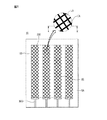
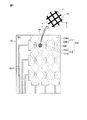
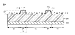
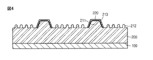
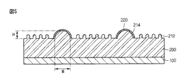
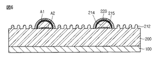
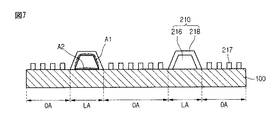
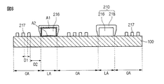
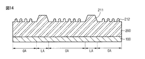
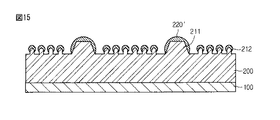
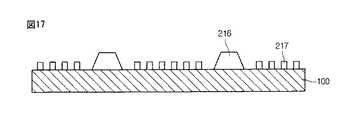
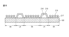
【解決手段】本発明によるタッチウィンドウは、基板と、基板の上に配置される電極部と、を含み、電極部は、第1サブパターン、第1サブパターンに配置される電極層、及び第1サブパターンに隣接して配置される第2サブパターンを含み、電極層と第1サブパターンとの間の境界面積が基板と第1サブパターンとの間の境界面積より大きい。本発明による従うタッチウィンドウは、基板と、基板の上に配置される電極部を含み、電極部は、第1サブパターン、第1サブパターンに配置される電極層、及び第1サブパターンに隣接して配置される第2サブパターンを含み、第1サブパターンの線幅は第1サブパターンの高さによって異なる。
【選択図】図2
Description
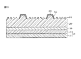
100 基板
200 電極部
300 配線
210 電極部
212 第1電極
214 第2電極
220 電極層
Claims (10)
- 基板と、
前記基板の上に配置される電極部と、を含み、
前記電極部は、
第1サブパターンと、
前記第1サブパターンに配置される電極層と、
前記第1サブパターンに隣接して配置される第2サブパターンと、を含み、
前記電極層と前記第1サブパターンとの間の境界面積が、前記基板と前記第1サブパターンとの間の境界面積より大きい、
ことを特徴とするタッチウィンドウ。 - 前記第1サブパターンの線幅は、前記第1サブパターンの高さによって異なる、請求項1に記載のタッチウィンドウ。
- 前記第1サブパターンの線幅は、前記第1サブパターンの高さが高くなるほど狭くなる、請求項1又は2に記載のタッチウィンドウ。
- 前記第1サブパターンは、上面及び側面を含み、
前記側面は、前記上面に対して傾いている、請求項1乃至3のいずれか一項に記載のタッチウィンドウ。 - 前記第1サブパターンは、曲面を含む、請求項1乃至4のいずれか一項に記載のタッチウィンドウ。
- 前記第1サブパターンの最も広い線幅及び高さの比は10:2から10:4の範囲である、請求項1乃至5のいずれか一項に記載のタッチウィンドウ。
- 前記第1サブパターンの上面に第3サブパターンを含む、請求項1乃至6のいずれか一項に記載のタッチウィンドウ。
- 前記第3サブパターンは、複数個の突起を含む、請求項7に記載のタッチウィンドウ。
- 前記電極部はメッシュ状に配置される、請求項1乃至8のいずれか一項に記載のタッチウィンドウ。
- 基板と、
前記基板の上に配置される電極部と、を含み、
前記電極部は、
第1サブパターンと、
前記第1サブパターンに配置される電極層と、
前記第1サブパターンに隣接して配置される第2サブパターンと、を含み、
前記第1サブパターンの線幅は前記第1サブパターンの高さによって異なる、
ことを特徴とするタッチウィンドウ。
Applications Claiming Priority (4)
| Application Number | Priority Date | Filing Date | Title |
|---|---|---|---|
| KR1020120133166A KR20140065999A (ko) | 2012-11-22 | 2012-11-22 | 터치 패널 및 이의 제조방법 |
| KR10-2012-0133166 | 2012-11-22 | ||
| KR10-2013-0083662 | 2013-07-16 | ||
| KR1020130083662A KR102098127B1 (ko) | 2013-07-16 | 2013-07-16 | 터치 윈도우 |
Publications (1)
| Publication Number | Publication Date |
|---|---|
| JP2014106974A true JP2014106974A (ja) | 2014-06-09 |
Family
ID=49765784
Family Applications (1)
| Application Number | Title | Priority Date | Filing Date |
|---|---|---|---|
| JP2013242029A Pending JP2014106974A (ja) | 2012-11-22 | 2013-11-22 | タッチウィンドウ |
Country Status (5)
| Country | Link |
|---|---|
| US (1) | US9560738B2 (ja) |
| EP (1) | EP2735950B1 (ja) |
| JP (1) | JP2014106974A (ja) |
| CN (1) | CN103838445B (ja) |
| TW (1) | TWI607542B (ja) |
Cited By (2)
| Publication number | Priority date | Publication date | Assignee | Title |
|---|---|---|---|---|
| WO2016151909A1 (ja) * | 2015-03-20 | 2016-09-29 | 富士フイルム株式会社 | 透明導電フィルムおよびタッチパネル |
| US10996805B2 (en) | 2017-08-10 | 2021-05-04 | Japan Display Inc. | Display device |
Families Citing this family (9)
| Publication number | Priority date | Publication date | Assignee | Title |
|---|---|---|---|---|
| TWI564766B (zh) * | 2014-11-09 | 2017-01-01 | 財團法人工業技術研究院 | 網狀電極、感測元件以及電極層 |
| US10001889B2 (en) | 2014-11-09 | 2018-06-19 | Industrial Technology Research Institute | Mesh electrode, sensing device, and electrode layer |
| EP3177117A4 (en) * | 2015-01-30 | 2017-12-20 | Fujikura, Ltd. | Wiring body, wiring substrate, and touch sensor |
| US20180074612A1 (en) * | 2015-02-27 | 2018-03-15 | Fujikura Ltd. | Wiring body, wiring board, touch sensor, and production method for wiring body |
| CN107250962A (zh) * | 2015-02-27 | 2017-10-13 | 株式会社藤仓 | 配线体、配线基板以及触摸传感器 |
| US20170293382A1 (en) * | 2015-05-01 | 2017-10-12 | Fujikura Ltd. | Wiring body, wiring board, and touch sensor |
| US20170269728A1 (en) * | 2016-03-15 | 2017-09-21 | Microsoft Technology Licensing, Llc | Rhombic mesh electrode matrix having periodic electrodes |
| CN107463296B (zh) * | 2017-09-21 | 2024-03-29 | 京东方科技集团股份有限公司 | 一种显示面板、触摸屏及显示装置 |
| DE102019114185B4 (de) * | 2019-05-27 | 2022-08-11 | Tacterion Gmbh | Taktiles Sensorelement |
Citations (11)
| Publication number | Priority date | Publication date | Assignee | Title |
|---|---|---|---|---|
| JP2006302930A (ja) * | 2005-04-15 | 2006-11-02 | Matsushita Electric Ind Co Ltd | 配線基板とそれを用いた電子部品実装体およびそれらの製造方法 |
| JP2008311416A (ja) * | 2007-06-14 | 2008-12-25 | Dainippon Printing Co Ltd | 金属転写箔を用いた電磁波シールドメッシュの製造方法、及び電磁波シールドメッシュ |
| JP2011096225A (ja) * | 2009-09-30 | 2011-05-12 | Dainippon Printing Co Ltd | タッチパネル用電極フィルム及びタッチパネル |
| US20110260741A1 (en) * | 2010-04-27 | 2011-10-27 | 3M Innovative Properties Company | Integrated passive circuit elements for sensing devices |
| WO2012063500A1 (ja) * | 2010-11-09 | 2012-05-18 | 株式会社翔栄 | タッチパネル及びタッチパネルの製造方法 |
| JP2012103761A (ja) * | 2010-11-05 | 2012-05-31 | Fujifilm Corp | タッチパネル |
| JP2012108845A (ja) * | 2010-11-19 | 2012-06-07 | Fujifilm Corp | タッチパネル用導電性フイルムを備えるタッチパネル及びタッチパネル用導電性フイルム |
| JP2012168301A (ja) * | 2011-02-14 | 2012-09-06 | Bridgestone Corp | 金属細線の形成方法及びこれを用いたワイヤグリッド型偏光子の製造方法 |
| JP2012198879A (ja) * | 2011-03-08 | 2012-10-18 | Fujifilm Corp | 抵抗膜式マルチタッチパネル及び抵抗膜式マルチタッチパネルに用いる電極シート |
| JP2012216450A (ja) * | 2011-04-01 | 2012-11-08 | Konica Minolta Holdings Inc | 導電性組成物の製造方法及びその導電性組成物を用いた透明導電膜、有機エレクトロルミネッセンス素子 |
| JP2012216084A (ja) * | 2011-03-31 | 2012-11-08 | Sony Corp | 情報入力装置 |
Family Cites Families (33)
| Publication number | Priority date | Publication date | Assignee | Title |
|---|---|---|---|---|
| JP2001075074A (ja) * | 1999-08-18 | 2001-03-23 | Internatl Business Mach Corp <Ibm> | タッチセンサ一体型液晶表示素子 |
| US8134652B2 (en) * | 2008-01-16 | 2012-03-13 | Samsung Electronics Co., Ltd. | Liquid crystal display having sensor and spacer arrangement and and method of manufacturing the same |
| JP2011517367A (ja) | 2008-02-28 | 2011-06-02 | スリーエム イノベイティブ プロパティズ カンパニー | 基材上に導電体をパターン化する方法 |
| KR101483626B1 (ko) * | 2008-06-09 | 2015-01-16 | 삼성디스플레이 주식회사 | 터치 스크린 표시 장치 |
| JP2010139525A (ja) * | 2008-12-09 | 2010-06-24 | Sony Corp | 表示装置、表示装置の駆動方法および電子機器 |
| JP5113773B2 (ja) * | 2009-01-20 | 2013-01-09 | 株式会社ジャパンディスプレイイースト | 表示装置 |
| KR101558915B1 (ko) * | 2009-03-27 | 2015-10-13 | 삼성디스플레이 주식회사 | 보호창을 갖는 터치 스크린 모듈 |
| KR101058106B1 (ko) * | 2009-08-06 | 2011-08-24 | 삼성모바일디스플레이주식회사 | 표시 장치 |
| JP5295914B2 (ja) * | 2009-09-18 | 2013-09-18 | 株式会社ジャパンディスプレイ | 表示装置 |
| CN102023770B (zh) * | 2009-09-22 | 2013-02-27 | 群康科技(深圳)有限公司 | 电容式触控面板模块及其制造方法 |
| US8493349B2 (en) * | 2009-12-10 | 2013-07-23 | Lg Display Co., Ltd. | Touch screen panel |
| US9152289B2 (en) * | 2009-12-11 | 2015-10-06 | Nissha Printing Co., Ltd. | Installation structure of thin-type display and resistive film type touch panel, resistive film type touch panel unit with front-surface protrusions, and thin-type display unit with back-surface protrusions |
| JP5413171B2 (ja) * | 2009-12-14 | 2014-02-12 | カシオ計算機株式会社 | タッチパネル |
| CN101738773B (zh) | 2009-12-30 | 2013-05-22 | 友达光电股份有限公司 | 触控式显示面板、像素结构以及多重感应结构 |
| US8780080B2 (en) * | 2010-02-24 | 2014-07-15 | Kyocera Corporation | Input device, display device and portable terminal |
| CN101788867B (zh) | 2010-03-12 | 2012-05-02 | 友达光电股份有限公司 | 感应结构及触控显示面板 |
| US20110146794A1 (en) * | 2010-03-17 | 2011-06-23 | Auria Solar Co., Ltd. | Thin-film solar cell and manufacture method thereof |
| CN102316675A (zh) * | 2010-06-30 | 2012-01-11 | 相互股份有限公司 | 电路板及其制造方法 |
| TWI427521B (zh) | 2010-09-15 | 2014-02-21 | Au Optronics Corp | 電容式觸控感測器及電容式觸控裝置 |
| KR101284714B1 (ko) * | 2010-09-20 | 2013-07-17 | 엘지디스플레이 주식회사 | 액정 표시장치와 이의 제조방법 |
| KR101284709B1 (ko) * | 2010-09-20 | 2013-07-16 | 엘지디스플레이 주식회사 | 액정 표시장치와 이의 제조방법 |
| WO2012056661A1 (ja) * | 2010-10-25 | 2012-05-03 | パナソニック株式会社 | 電子部品の接合形態 |
| KR101742753B1 (ko) * | 2010-10-29 | 2017-06-02 | 삼성디스플레이 주식회사 | 터치 패널, 표시 장치 및 터치 패널의 제조 방법 |
| KR101295535B1 (ko) * | 2010-11-22 | 2013-08-12 | 엘지디스플레이 주식회사 | 액정표시장치 및 그 제조방법 |
| KR101284287B1 (ko) * | 2010-12-21 | 2013-07-08 | 엘지디스플레이 주식회사 | 액정 표시장치와 이의 제조방법 |
| TWI595403B (zh) | 2011-03-29 | 2017-08-11 | 元太科技工業股份有限公司 | 觸控式彩色面板、觸控式電泳彩色顯示面板及其裝置 |
| KR20130043526A (ko) * | 2011-10-20 | 2013-04-30 | 삼성전자주식회사 | 플렉시블 표시장치 |
| US9262019B2 (en) * | 2011-11-22 | 2016-02-16 | Atmel Corporation | Touch sensor with conductive lines having different widths |
| US20130161070A1 (en) * | 2011-12-21 | 2013-06-27 | Samsung Electro-Mechanics Co., Ltd. | Touch panel and method for manufacturing the same |
| TWM448733U (zh) * | 2012-06-21 | 2013-03-11 | Eturbotouch Technology Inc | 多功能單基材的觸控面板 |
| US9110545B2 (en) * | 2012-08-16 | 2015-08-18 | Nokia Technologies Oy | Apparatus and associated methods |
| KR101930383B1 (ko) * | 2012-10-31 | 2019-03-11 | 엘지디스플레이 주식회사 | 유기발광장치 및 그 제조방법 |
| KR102175045B1 (ko) * | 2013-01-25 | 2020-11-06 | 삼성디스플레이 주식회사 | 터치 스크린 패널 |
-
2013
- 2013-11-22 JP JP2013242029A patent/JP2014106974A/ja active Pending
- 2013-11-22 EP EP13194107.2A patent/EP2735950B1/en not_active Not-in-force
- 2013-11-22 TW TW102142610A patent/TWI607542B/zh not_active IP Right Cessation
- 2013-11-22 CN CN201310596209.4A patent/CN103838445B/zh not_active Expired - Fee Related
- 2013-11-22 US US14/087,496 patent/US9560738B2/en not_active Expired - Fee Related
Patent Citations (11)
| Publication number | Priority date | Publication date | Assignee | Title |
|---|---|---|---|---|
| JP2006302930A (ja) * | 2005-04-15 | 2006-11-02 | Matsushita Electric Ind Co Ltd | 配線基板とそれを用いた電子部品実装体およびそれらの製造方法 |
| JP2008311416A (ja) * | 2007-06-14 | 2008-12-25 | Dainippon Printing Co Ltd | 金属転写箔を用いた電磁波シールドメッシュの製造方法、及び電磁波シールドメッシュ |
| JP2011096225A (ja) * | 2009-09-30 | 2011-05-12 | Dainippon Printing Co Ltd | タッチパネル用電極フィルム及びタッチパネル |
| US20110260741A1 (en) * | 2010-04-27 | 2011-10-27 | 3M Innovative Properties Company | Integrated passive circuit elements for sensing devices |
| JP2012103761A (ja) * | 2010-11-05 | 2012-05-31 | Fujifilm Corp | タッチパネル |
| WO2012063500A1 (ja) * | 2010-11-09 | 2012-05-18 | 株式会社翔栄 | タッチパネル及びタッチパネルの製造方法 |
| JP2012108845A (ja) * | 2010-11-19 | 2012-06-07 | Fujifilm Corp | タッチパネル用導電性フイルムを備えるタッチパネル及びタッチパネル用導電性フイルム |
| JP2012168301A (ja) * | 2011-02-14 | 2012-09-06 | Bridgestone Corp | 金属細線の形成方法及びこれを用いたワイヤグリッド型偏光子の製造方法 |
| JP2012198879A (ja) * | 2011-03-08 | 2012-10-18 | Fujifilm Corp | 抵抗膜式マルチタッチパネル及び抵抗膜式マルチタッチパネルに用いる電極シート |
| JP2012216084A (ja) * | 2011-03-31 | 2012-11-08 | Sony Corp | 情報入力装置 |
| JP2012216450A (ja) * | 2011-04-01 | 2012-11-08 | Konica Minolta Holdings Inc | 導電性組成物の製造方法及びその導電性組成物を用いた透明導電膜、有機エレクトロルミネッセンス素子 |
Cited By (4)
| Publication number | Priority date | Publication date | Assignee | Title |
|---|---|---|---|---|
| WO2016151909A1 (ja) * | 2015-03-20 | 2016-09-29 | 富士フイルム株式会社 | 透明導電フィルムおよびタッチパネル |
| JPWO2016151909A1 (ja) * | 2015-03-20 | 2017-08-10 | 富士フイルム株式会社 | 透明導電フィルムおよびタッチパネル |
| US10437093B2 (en) | 2015-03-20 | 2019-10-08 | Fujifilm Corporation | Transparent conductive film and touch panel |
| US10996805B2 (en) | 2017-08-10 | 2021-05-04 | Japan Display Inc. | Display device |
Also Published As
| Publication number | Publication date |
|---|---|
| EP2735950B1 (en) | 2019-04-03 |
| CN103838445B (zh) | 2017-06-13 |
| TW201431034A (zh) | 2014-08-01 |
| TWI607542B (zh) | 2017-12-01 |
| CN103838445A (zh) | 2014-06-04 |
| US20140138143A1 (en) | 2014-05-22 |
| EP2735950A2 (en) | 2014-05-28 |
| EP2735950A3 (en) | 2017-11-01 |
| US9560738B2 (en) | 2017-01-31 |
Similar Documents
| Publication | Publication Date | Title |
|---|---|---|
| KR102108846B1 (ko) | 터치 윈도우 | |
| CN103838445B (zh) | 触窗 | |
| JP6336744B2 (ja) | 電極部材及びこれを含むタッチパネル | |
| TWI634471B (zh) | 觸控面板與具有其之觸控裝置 | |
| JP2015053055A (ja) | タッチウィンドウ及びこれを含むタッチデバイス | |
| KR102191575B1 (ko) | 터치 윈도우 및 이를 포함하는 디스플레이 장치 | |
| KR20150103977A (ko) | 터치 윈도우 및 이를 포함하는 디스플레이 장치 | |
| TW201506753A (zh) | 觸控視窗以及包含其之觸控裝置 | |
| US20170329455A1 (en) | Touch panel and touch display screen | |
| KR102053238B1 (ko) | 터치 윈도우 | |
| US9442613B2 (en) | Touch window | |
| KR20140039914A (ko) | 터치 패널 및 이의 제조방법 | |
| KR102237797B1 (ko) | 터치 윈도우 및 이를 포함하는 디스플레이 장치 | |
| KR102098127B1 (ko) | 터치 윈도우 | |
| KR102074875B1 (ko) | 터치 윈도우 | |
| KR102108843B1 (ko) | 터치 윈도우 | |
| KR102053230B1 (ko) | 터치 패널 | |
| KR102019059B1 (ko) | 터치 윈도우 | |
| KR102237791B1 (ko) | 터치 윈도우 | |
| KR20150084542A (ko) | 터치 윈도우 및 이를 포함하는 디스플레이 장치 | |
| KR102131256B1 (ko) | 터치 윈도우 및 이를 포함하는 터치 디바이스 | |
| KR20150087942A (ko) | 터치 윈도우 및 이를 포함하는 디스플레이 장치 | |
| KR20150014375A (ko) | 터치 윈도우 및 이의 제조방법 | |
| KR20160039426A (ko) | 터치 윈도우 | |
| KR20140065999A (ko) | 터치 패널 및 이의 제조방법 |
Legal Events
| Date | Code | Title | Description |
|---|---|---|---|
| A621 | Written request for application examination |
Free format text: JAPANESE INTERMEDIATE CODE: A621 Effective date: 20161110 |
|
| A977 | Report on retrieval |
Free format text: JAPANESE INTERMEDIATE CODE: A971007 Effective date: 20170831 |
|
| A131 | Notification of reasons for refusal |
Free format text: JAPANESE INTERMEDIATE CODE: A131 Effective date: 20170905 |
|
| A521 | Request for written amendment filed |
Free format text: JAPANESE INTERMEDIATE CODE: A523 Effective date: 20171205 |
|
| A02 | Decision of refusal |
Free format text: JAPANESE INTERMEDIATE CODE: A02 Effective date: 20180327 |