JP2014130077A - Pattern shape evaluation method, semiconductor device manufacturing method, and pattern shape evaluation device - Google Patents
Pattern shape evaluation method, semiconductor device manufacturing method, and pattern shape evaluation device Download PDFInfo
- Publication number
- JP2014130077A JP2014130077A JP2012287906A JP2012287906A JP2014130077A JP 2014130077 A JP2014130077 A JP 2014130077A JP 2012287906 A JP2012287906 A JP 2012287906A JP 2012287906 A JP2012287906 A JP 2012287906A JP 2014130077 A JP2014130077 A JP 2014130077A
- Authority
- JP
- Japan
- Prior art keywords
- substrate
- obtaining
- pattern
- edge
- pattern shape
- Prior art date
- Legal status (The legal status is an assumption and is not a legal conclusion. Google has not performed a legal analysis and makes no representation as to the accuracy of the status listed.)
- Pending
Links
Images


Classifications
-
- H—ELECTRICITY
- H01—ELECTRIC ELEMENTS
- H01J—ELECTRIC DISCHARGE TUBES OR DISCHARGE LAMPS
- H01J37/00—Discharge tubes with provision for introducing objects or material to be exposed to the discharge, e.g. for the purpose of examination or processing thereof
- H01J37/26—Electron or ion microscopes; Electron or ion diffraction tubes
- H01J37/285—Emission microscopes, e.g. field-emission microscopes
-
- H—ELECTRICITY
- H01—ELECTRIC ELEMENTS
- H01J—ELECTRIC DISCHARGE TUBES OR DISCHARGE LAMPS
- H01J37/00—Discharge tubes with provision for introducing objects or material to be exposed to the discharge, e.g. for the purpose of examination or processing thereof
- H01J37/02—Details
- H01J37/22—Optical, image processing or photographic arrangements associated with the tube
- H01J37/222—Image processing arrangements associated with the tube
-
- H—ELECTRICITY
- H01—ELECTRIC ELEMENTS
- H01J—ELECTRIC DISCHARGE TUBES OR DISCHARGE LAMPS
- H01J37/00—Discharge tubes with provision for introducing objects or material to be exposed to the discharge, e.g. for the purpose of examination or processing thereof
- H01J37/26—Electron or ion microscopes; Electron or ion diffraction tubes
- H01J37/261—Details
- H01J37/265—Controlling the tube; circuit arrangements adapted to a particular application not otherwise provided, e.g. bright-field-dark-field illumination
-
- H—ELECTRICITY
- H01—ELECTRIC ELEMENTS
- H01J—ELECTRIC DISCHARGE TUBES OR DISCHARGE LAMPS
- H01J37/00—Discharge tubes with provision for introducing objects or material to be exposed to the discharge, e.g. for the purpose of examination or processing thereof
- H01J37/26—Electron or ion microscopes; Electron or ion diffraction tubes
- H01J37/28—Electron or ion microscopes; Electron or ion diffraction tubes with scanning beams
-
- H—ELECTRICITY
- H10—SEMICONDUCTOR DEVICES; ELECTRIC SOLID-STATE DEVICES NOT OTHERWISE PROVIDED FOR
- H10P—GENERIC PROCESSES OR APPARATUS FOR THE MANUFACTURE OR TREATMENT OF DEVICES COVERED BY CLASS H10
- H10P74/00—Testing or measuring during manufacture or treatment of wafers, substrates or devices
- H10P74/20—Testing or measuring during manufacture or treatment of wafers, substrates or devices characterised by the properties tested or measured, e.g. structural or electrical properties
- H10P74/203—Structural properties, e.g. testing or measuring thicknesses, line widths, warpage, bond strengths or physical defects
-
- G—PHYSICS
- G01—MEASURING; TESTING
- G01B—MEASURING LENGTH, THICKNESS OR SIMILAR LINEAR DIMENSIONS; MEASURING ANGLES; MEASURING AREAS; MEASURING IRREGULARITIES OF SURFACES OR CONTOURS
- G01B15/00—Measuring arrangements characterised by the use of electromagnetic waves or particle radiation, e.g. by the use of microwaves, X-rays, gamma rays or electrons
- G01B15/04—Measuring arrangements characterised by the use of electromagnetic waves or particle radiation, e.g. by the use of microwaves, X-rays, gamma rays or electrons for measuring contours or curvatures
-
- G—PHYSICS
- G01—MEASURING; TESTING
- G01B—MEASURING LENGTH, THICKNESS OR SIMILAR LINEAR DIMENSIONS; MEASURING ANGLES; MEASURING AREAS; MEASURING IRREGULARITIES OF SURFACES OR CONTOURS
- G01B2210/00—Aspects not specifically covered by any group under G01B, e.g. of wheel alignment, caliper-like sensors
- G01B2210/56—Measuring geometric parameters of semiconductor structures, e.g. profile, critical dimensions or trench depth
-
- H—ELECTRICITY
- H01—ELECTRIC ELEMENTS
- H01J—ELECTRIC DISCHARGE TUBES OR DISCHARGE LAMPS
- H01J2237/00—Discharge tubes exposing object to beam, e.g. for analysis treatment, etching, imaging
- H01J2237/22—Treatment of data
- H01J2237/221—Image processing
-
- H—ELECTRICITY
- H01—ELECTRIC ELEMENTS
- H01J—ELECTRIC DISCHARGE TUBES OR DISCHARGE LAMPS
- H01J2237/00—Discharge tubes exposing object to beam, e.g. for analysis treatment, etching, imaging
- H01J2237/245—Detection characterised by the variable being measured
- H01J2237/24571—Measurements of non-electric or non-magnetic variables
- H01J2237/24578—Spatial variables, e.g. position, distance
-
- H—ELECTRICITY
- H01—ELECTRIC ELEMENTS
- H01J—ELECTRIC DISCHARGE TUBES OR DISCHARGE LAMPS
- H01J2237/00—Discharge tubes exposing object to beam, e.g. for analysis treatment, etching, imaging
- H01J2237/245—Detection characterised by the variable being measured
- H01J2237/24592—Inspection and quality control of devices
Landscapes
- Chemical & Material Sciences (AREA)
- Analytical Chemistry (AREA)
- Engineering & Computer Science (AREA)
- Computer Vision & Pattern Recognition (AREA)
- Length-Measuring Devices Using Wave Or Particle Radiation (AREA)
- Physics & Mathematics (AREA)
- Electromagnetism (AREA)
- General Physics & Mathematics (AREA)
- Exposure And Positioning Against Photoresist Photosensitive Materials (AREA)
- Testing Or Measuring Of Semiconductors Or The Like (AREA)
Abstract
【課題】ウエハの上方から観察した回路パターンの平面像のみから、回路パターンの断面形状又は3次元形状を推定し評価する。
【解決手段】本発明は、立体的な構造体が上面に形成された基板の主面に略垂直な方向から収束エネルギー線を照射するとともに上記基板の上面を走査させ、上記基板及び上記構造体から発生した2次エネルギー線又は上記基板及び上記構造体により反射若しくは散乱されたエネルギー線の強度を検出及び/又は測定し、上記構造体の上面観察像を取得する処理と、上記上面観察像における収束エネルギー線の照射位置と測定された上記強度から上記構造体の表面の凹凸形状による散乱強度の不確かさ情報を求める処理と、求めた上記不確かさ情報に基づいて上記構造体の表面の傾斜角度θを求める処理と、求めた傾斜角度θに基づいて上記構造体の立体形状を推定する処理とを有する。
【選択図】図14A cross-sectional shape or a three-dimensional shape of a circuit pattern is estimated and evaluated only from a planar image of the circuit pattern observed from above the wafer.
The present invention irradiates a convergent energy beam from a direction substantially perpendicular to a main surface of a substrate having a three-dimensional structure formed on the upper surface, and scans the upper surface of the substrate, thereby the substrate and the structure. A process of detecting and / or measuring the intensity of secondary energy rays generated from the substrate or energy rays reflected or scattered by the substrate and the structure, and obtaining a top surface observation image of the structure; Processing for obtaining uncertainty information on the scattering intensity due to the uneven shape of the surface of the structure from the irradiation position of the convergent energy beam and the measured intensity, and the inclination angle of the surface of the structure based on the obtained uncertainty information a process of obtaining θ and a process of estimating the three-dimensional shape of the structure based on the obtained inclination angle θ.
[Selection] Figure 14
Description
本発明は、例えば走査型顕微鏡を用いた非破壊観測及び画像処理による詳細な形状評価方法、そのための装置、及び、当該技術を採用する半導体装置の製造方法に関する。 The present invention relates to a detailed shape evaluation method by non-destructive observation and image processing using, for example, a scanning microscope, an apparatus therefor, and a method for manufacturing a semiconductor device employing the technique.
半導体集積回路(LSI)は、回路パターンの微細化による高性能化・高集積化が進んでいる。現在、最先端LSIの最小回路パターンの線幅は30nm(ナノメートル)以下であり、LSIの性能を確保するためには、これらの回路寸法を厳密に(例えば寸法のバラツキ変動の許容値が設計値の1割以下となるような精度で)管理する必要がある。上記回路寸法の測定には現在広く走査型電子顕微鏡(SEM)が用いられている。非特許文献1には、ウエハを上面から観察する回路寸法計測専用の電界放出型電子顕微鏡(CD-SEM: Critical Dimension SEM)について記載されている。
Semiconductor integrated circuits (LSIs) have been improved in performance and integration by miniaturizing circuit patterns. At present, the line width of the smallest circuit pattern of the most advanced LSI is 30 nm (nanometer) or less, and in order to ensure the performance of the LSI, these circuit dimensions are strictly designed (for example, the tolerance of variation in the dimensions is designed. It must be managed (with a precision that is less than 10% of the value). Currently, a scanning electron microscope (SEM) is widely used to measure the circuit dimensions. Non-Patent
上記CD-SEMは、半導体回路の線幅測定の他、様々な特徴量を計測するために用いられている。例えば、上記回路パターンのエッジにはラインエッジラフネス(LER)と呼ばれる凹凸が存在し、回路性能に悪影響を及ぼすことが知られている。CD-SEMは上記LERの計測に広く用いられており、例えば特許文献1にはその測定方法が記載されている。
The CD-SEM is used for measuring various feature quantities in addition to measuring the line width of a semiconductor circuit. For example, it is known that the edge of the circuit pattern has irregularities called line edge roughness (LER), which adversely affects circuit performance. CD-SEM is widely used for the measurement of the LER. For example,
その一方で、ウエハ上に積層・パターニングにより形成された素子構造の立体的な形状を知りたいという要求がある。特に、LSIの量産工程では、断面観察によらず非破壊でこれを行うことが望ましいが、このための手法として、一般にAFM又は光学的方法(Scatterometry)が用いられている。 On the other hand, there is a demand for knowing the three-dimensional shape of the element structure formed on the wafer by lamination and patterning. In particular, in the mass production process of LSI, it is desirable to do this non-destructively regardless of cross-sectional observation. As a technique for this purpose, AFM or optical method (Scatterometry) is generally used.
AFMは、微細な先端をもつ探針により、探針先端と試料表面の間の原子間力が一定になるように走査することにより、試料表面の凹凸形状を計測する方法である。その詳細は、例えば特許文献2に記載されている。
AFM is a method for measuring the concavo-convex shape of the sample surface by scanning with a probe having a fine tip so that the atomic force between the tip of the probe and the sample surface is constant. The details are described in
Scatterometryは、周期的立体構造をもつパターンに光を入射してその反射回折光の波長又は回折角依存性を測定し、これをあらかじめ様々な断面形状に対して計算により求めた回折角依存性と比較することにより立体構造の断面形状を推定する。Scatterometryについては、例えば非特許文献2に記載されている。
Scatterometry measures the wavelength or diffraction angle dependence of the reflected diffracted light by making light incident on a pattern having a periodic three-dimensional structure, and this is the diffraction angle dependence obtained by calculation for various cross-sectional shapes in advance. By comparing, the cross-sectional shape of the three-dimensional structure is estimated. Scatterometry is described in
Scatterometryと類似の手法であって、SEMを用いて断面形状を推定する方法に、MBL(model-based library)法がある。MBL法は、試料に収束電子ビームを走査して得られる2次電子検出信号強度分布と、予め様々な断面形状に対して計算により求めた2次電子信号強度分布との比較により、立体構造の断面形状を推定する。MBLについては、例えば特許文献3又は非特許文献3に記載されている。
An MBL (model-based library) method is a method similar to Scatterometry that estimates the cross-sectional shape using SEM. The MBL method is based on the comparison of the secondary electron detection signal intensity distribution obtained by scanning the sample with a focused electron beam and the secondary electron signal intensity distribution obtained by calculation for various cross-sectional shapes in advance. Estimate the cross-sectional shape. About MBL, it describes in the
また、SEMを用いて立体構造を測定する方法として、tilt-SEMがある。この方法はウエハに対して異なる角度から電子線を入射して得られた複数の像からステレオ画像の原理により3次元形状を推測する。tilt-SEMについては、例えば特許文献4に記載されている。
Moreover, there is tilt-SEM as a method for measuring a three-dimensional structure using SEM. In this method, a three-dimensional shape is estimated based on the principle of a stereo image from a plurality of images obtained by making an electron beam incident on the wafer from different angles. About tilt-SEM, it describes in the
半導体集積回路(LSI)の製造工程では、回路パターン又はこれを形成するためのレジストパターン等の断面形状、もしくは3次元形状を所定の設計範囲内に管理することが重要である。これらの形状が設計値通りとなるように製造条件を設定したり、形状が劣化した場合には、いち早くこれを検知し、製造プロセスへフィードバックすることで品質劣化を抑制する必要がある。 In the manufacturing process of a semiconductor integrated circuit (LSI), it is important to manage a cross-sectional shape such as a circuit pattern or a resist pattern for forming the circuit pattern, or a three-dimensional shape within a predetermined design range. It is necessary to set the manufacturing conditions so that these shapes conform to the design values, or when the shape deteriorates, quickly detect this and feed back to the manufacturing process to suppress the quality deterioration.
しかし、現在まで、任意形状の微細な回路パターンの断面形状又は3次元形状を、非破壊、高精度かつ簡便に計測できる手法が存在しないという技術課題があった。例えばCD-SEMは、任意形状の微細な回路パターンの寸法を非破壊、高精度かつ簡便に計測できるが、ウエハの上方から回路の平面形状を観察するために、断面形状の推定が困難であるという技術課題を有している。 However, until now, there has been a technical problem that there is no method capable of measuring a cross-sectional shape or a three-dimensional shape of a fine circuit pattern of an arbitrary shape in a non-destructive manner, with high accuracy and simply. For example, CD-SEM can measure the dimensions of minute circuit patterns of any shape in a non-destructive, high-precision and simple manner, but it is difficult to estimate the cross-sectional shape because the planar shape of the circuit is observed from above the wafer. It has a technical problem.
そこで一般には、ウエハを破壊して回路パターンの断面を露出し、その断面形状を電子顕微鏡で観察する手法が用いられる。ところが、製品ウエハに対し、この手法を適用することは難しい。このように、従来、CD-SEMを用いた断面形状の推定は困難であると考えられており、前述したような各種の方法が試みられてきた。 Therefore, generally, a technique is used in which a wafer is broken to expose a cross section of a circuit pattern and the cross section is observed with an electron microscope. However, it is difficult to apply this method to product wafers. Thus, it has been conventionally considered that estimation of a cross-sectional shape using a CD-SEM is difficult, and various methods as described above have been tried.
しかし、そのいずれの方法においても、以下のような技術上の課題がある。
例えばAFMによる方法では、回路パターンの寸法が縮小するのに伴い、探針がパターン間に入り込むことができず、形状測定が困難になるという課題がある。
However, both methods have the following technical problems.
For example, the AFM method has a problem that, as the size of the circuit pattern is reduced, the probe cannot enter between the patterns and the shape measurement becomes difficult.
また、scatterometry又はMBLによる方法では、様々な断面形状に対して予想される測定結果を予め計算により求めてライブラリとして用意する必要がある。しかし、これには膨大な計算を要し、適用可能な形状が台形等の比較的単純形状に限定されるという課題がある。特に、scatterometryによる方法では、被計測パターンが、数十ミクロン角の広い領域内に一様に存在する周期パターンに限定されるため、論理LSIの回路のような不規則的なパターンの断面形状を推定することが困難である。また、同方法は、計測パターンのために専用の広い領域を確保する必要があるという課題がある。 In addition, in the method using scatterometry or MBL, it is necessary to prepare in advance a measurement result expected for various cross-sectional shapes by calculation and prepare it as a library. However, this requires enormous calculations, and there is a problem that applicable shapes are limited to relatively simple shapes such as trapezoids. In particular, with the scatterometry method, the pattern to be measured is limited to a periodic pattern that exists uniformly within a wide area of several tens of microns, so the cross-sectional shape of an irregular pattern such as a logic LSI circuit can be reduced. It is difficult to estimate. In addition, this method has a problem that it is necessary to secure a dedicated wide area for the measurement pattern.
また、tilt-SEMを用いる方法では、収束電子線の入射角を変化させるための特殊な電子光学系が必要とされ、一般に、分解能等の性能が劣化する等の課題がある。また、ステージを傾けるために装置が大型化するという課題、計測に時間を要するという課題等も存在する。 In addition, the method using tilt-SEM requires a special electron optical system for changing the incident angle of the convergent electron beam, and generally has problems such as degradation in performance such as resolution. In addition, there are a problem that the apparatus becomes large in order to tilt the stage, a problem that the measurement takes time, and the like.
そこで、本発明は、荷電粒子線装置を用いて取得した基板の上面からの観察像だけを用いつつ、基板の上面に形成された任意の構造体の断面形状を非破壊かつ高精度で推定できる技術を提供する。 Therefore, the present invention can estimate the cross-sectional shape of an arbitrary structure formed on the upper surface of the substrate with high accuracy while using only the observation image from the upper surface of the substrate acquired using the charged particle beam apparatus. Provide technology.
上記課題を解決するために、例えば特許請求の範囲に記載の構成を採用する。一例としての発明は、(a) 立体的な構造体が上面に形成された基板の主面に略垂直な方向から収束エネルギー線を照射するとともに上記基板の上面を走査させ、上記基板及び上記構造体から発生した2次エネルギー線又は上記基板及び上記構造体により反射若しくは散乱されたエネルギー線の強度を検出及び/又は測定し、上記構造体の上面観察像を取得する処理と、(b) 上記上面観察像における収束エネルギー線照射位置と測定された上記強度から上記構造体の表面の凹凸形状による散乱強度の不確かさ情報を求める処理と、(c) 求めた上記不確かさ情報に基づいて上記構造体の表面の傾斜角度θを求める処理と、(d) 求めた傾斜角度θに基づいて上記構造体の立体形状を推定する処理とを有する。 In order to solve the above problems, for example, the configuration described in the claims is adopted. The invention as an example includes: (a) irradiating a convergent energy beam from a direction substantially perpendicular to a main surface of a substrate on which a three-dimensional structure is formed, and scanning the upper surface of the substrate; A process of detecting and / or measuring the intensity of secondary energy rays generated from a body or energy rays reflected or scattered by the substrate and the structure, and obtaining an upper surface observation image of the structure; and (b) the above A process for obtaining uncertainty information of scattering intensity due to the uneven shape of the surface of the structure from the focused energy ray irradiation position in the upper surface observation image and the measured intensity, and (c) the structure based on the obtained uncertainty information. A process for obtaining the inclination angle θ of the body surface, and (d) a process for estimating the three-dimensional shape of the structure based on the obtained inclination angle θ.
本発明によれば、基板の上面観察像のみから、基板の上面に形成された構造体の断面形状又は3次元形状を推定し評価することができる。前述した以外の課題、構成及び効果は、以下の実施形態の説明により明らかにされる。 According to the present invention, it is possible to estimate and evaluate the cross-sectional shape or three-dimensional shape of the structure formed on the upper surface of the substrate only from the upper surface observation image of the substrate. Problems, configurations, and effects other than those described above will become apparent from the following description of embodiments.
以下、図面に基づいて、本発明の実施の形態を説明する。なお、本発明の実施態様は、後述する形態例に限定されるものではなく、その技術思想の範囲において、種々の変形が可能である。例えば以下の説明では電子顕微鏡を用いて試料を観察する場合について説明するが、集束イオンビーム装置その他の荷電粒子線装置を用いて試料を観察する場合や加工する場合についても同様に適用することができる。 Hereinafter, embodiments of the present invention will be described with reference to the drawings. The embodiment of the present invention is not limited to the embodiments described later, and various modifications can be made within the scope of the technical idea. For example, in the following description, the case of observing a sample using an electron microscope will be described, but the same applies to the case of observing or processing a sample using a focused ion beam device or other charged particle beam device. it can.
(3次元形状観察像におけるエッジ変動要因とその成分分解)
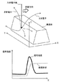
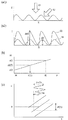
まず、本発明で用いる電子顕微鏡による観察像の形成過程を、図1を用いて説明する。単純化のため、基板面上に形成された略立方体状の構造体(例えば半導体やレジストパターン等)を考える。基板面をx−y平面、構造体のエッジの延びる方向(エッジ方向)をy方向とする。上記構造体の特徴寸法より十分に細く収束された電子線を、上記基板面と略垂直な方向(z方向)から基板上に照射すると共に、基板上を上記エッジ方向と略垂直な方向(x方向)に走査する。上記基板又は構造体に入射した電子は、基板又は構造体内部で散乱を受けて2次電子を放出し、又は直接反射(又は後方散乱)され、その一部を基板又は構造体の外部へ放出する。上記2次電子又は反射電子(以下、「2次電子等」という)の放出量は、電子線が凸形状の凸部(又は角の上部)に入射した場合に増大する。
(Edge variation factor and its component decomposition in 3D shape observation image)
First, the process of forming an observation image by an electron microscope used in the present invention will be described with reference to FIG. For the sake of simplicity, a substantially cubic structure (for example, a semiconductor or a resist pattern) formed on the substrate surface is considered. The substrate surface is defined as the xy plane, and the direction in which the edge of the structure extends (edge direction) is defined as the y direction. An electron beam converged sufficiently narrower than the characteristic dimension of the structure is irradiated onto the substrate from a direction (z direction) substantially perpendicular to the substrate surface, and the direction on the substrate is substantially perpendicular to the edge direction (x Direction). Electrons incident on the substrate or structure are scattered inside the substrate or structure to emit secondary electrons, or directly reflected (or backscattered), and part of the electrons are emitted to the outside of the substrate or structure. To do. The amount of secondary electrons or reflected electrons (hereinafter referred to as “secondary electrons”) is increased when an electron beam is incident on a convex portion (or an upper portion of a corner).
そこで、電子線の走査中に放出された上記2次電子等を検出器で検出し、その検出強度を走査方向における電子線の照射位置xに対してプロットすると、図1の下段に示すような2次電子等の検出信号強度分布が得られる。一般に、検出信号強度分布を検出信号の最大値で規格化したときの所定のしきい値レベルで切った時の位置、又は、検出信号強度分布の傾斜が最大となる位置等に基づいてパターン及び非パターンの境界を決定する。2つのパターン境界位置間の距離からパターン寸法が計測される。また、走査をエッジ方向(y方向)の異なる位置で行い、求めたパターン/非パターン境界を結ぶことによりパターンのエッジ形状が得られる。通常、このようにして得られたエッジ形状は、エッジ方向に沿って凹凸状を呈する。この凹凸の大きさをラインエッジラフネスと呼ぶ。本発明者は、上記ラフネスの原因を考察することにより、パターンエッジに平行な方向及び垂直な方向を含む平面(以下、「基板面」という)内の検出信号強度分布から、上記基板面に垂直な方向のパターンの立体形状を推定する方法を考案した。 Therefore, when the secondary electrons and the like emitted during scanning of the electron beam are detected by a detector and the detected intensity is plotted against the irradiation position x of the electron beam in the scanning direction, as shown in the lower part of FIG. A detection signal intensity distribution of secondary electrons or the like is obtained. Generally, a pattern based on the position when the detection signal intensity distribution is cut at a predetermined threshold level when the detection signal intensity distribution is normalized by the maximum value of the detection signal, or the position where the inclination of the detection signal intensity distribution is maximum Determine non-pattern boundaries. The pattern dimension is measured from the distance between the two pattern boundary positions. Further, scanning is performed at different positions in the edge direction (y direction), and the edge shape of the pattern is obtained by connecting the obtained pattern / non-pattern boundary. Usually, the edge shape obtained in this way exhibits an uneven shape along the edge direction. The size of this unevenness is called line edge roughness. The present inventor considers the cause of the roughness, and from the detection signal intensity distribution in a plane (hereinafter referred to as “substrate surface”) including a direction parallel to the pattern edge and a direction perpendicular to the pattern edge, We devised a method for estimating the three-dimensional shape of patterns in various directions.
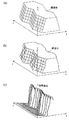
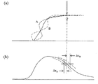
上述したラインエッジラフネスは、一般的に、図2の上段図(a)に示すような構造体のエッジ位置のばらつきに起因するものと考えられている。実際の構造体は立方体ではなく、その側壁は図2の上段図(a)に示すように傾斜しており、又は、図2の中段図(b)に示すように表面に凹凸(表面ラフネス)を有する。検出信号強度分布は、傾斜角の変化や表面の凹凸の影響を受けると考えられる。 The above-described line edge roughness is generally considered to be caused by variations in the edge position of the structure as shown in the upper diagram (a) of FIG. The actual structure is not a cube, and its side wall is inclined as shown in the upper diagram (a) of FIG. 2, or the surface is uneven (surface roughness) as shown in the middle diagram (b) of FIG. Have The detection signal intensity distribution is considered to be affected by changes in the tilt angle and surface irregularities.
y方向について一定のサンプリング間隔で規定された開始点からx方向に電子線を走査して2次電子検出信号強度を計測すると、図2の下段図(c)に示すような2次電子検出信号強度の2次元分布が得られる。ここで、2次電子検出信号強度の2次元分布は、(1)構造体の立体形状及び材料特性に起因する強度変化、(2)エッジ方向に沿った構造体のx方向位置変動による強度分布の変動、(3)構造体表面の凹凸に起因する強度分布の変動の3つの要因の影響を受けると考えられる。 When the secondary electron detection signal intensity is measured by scanning the electron beam in the x direction from the start point defined at a constant sampling interval in the y direction, the secondary electron detection signal as shown in the lower diagram (c) of FIG. A two-dimensional distribution of intensity is obtained. Here, the two-dimensional distribution of the secondary electron detection signal intensity includes (1) intensity change caused by the three-dimensional shape and material characteristics of the structure, and (2) intensity distribution due to the x-direction position fluctuation of the structure along the edge direction. And (3) the influence of three factors of the intensity distribution due to the unevenness of the structure surface.
そこで、これらの3つの要因を分解して考える。まず、y座標を固定して、xz平面でパターンを切断した時の断面形状と、当該形状に対応する1次元信号強度分布について考える。この場合、図2の中段図(b)の構造体は、図3の上段図(a)の左側に模式的に示すようなマクロなパターン構造の表面に、図3の中断図(b)の左側に模式的に示すようなミクロな表面の凹凸構造が重なった形状を有するものと考えられる。図3の下段図(c)の左側にマクロパターンとミクロパターンが重畳したイメージを示す。 Therefore, these three factors are disaggregated and considered. First, consider the cross-sectional shape when the y coordinate is fixed and the pattern is cut on the xz plane, and the one-dimensional signal intensity distribution corresponding to the shape. In this case, the structure of the middle diagram (b) of FIG. 2 is placed on the surface of the macro pattern structure as schematically shown on the left side of the upper diagram (a) of FIG. It is thought that it has a shape in which microscopic surface uneven structures as schematically shown on the left side overlap. An image in which a macro pattern and a micro pattern are superimposed is shown on the left side of the lower diagram (c) of FIG.
前述したように、2次電子放出量は、電子線が凸部に入射すると増大し、逆に電子線が凹部に入射すると減少する。従って、パターン全体のマクロな構造を見ると、パターンの上面角部は凸形状なので、上面角部へ向かって信号強度が増大する(図3の上段図(a)の右側)。一方、ミクロな構造を見ると、パターン表面に存在する凹凸の凸部に入射したとき、信号強度は増大する(図3の中段図(b)の右側)。従って、これに対応して2次電子信号強度分布は、マクロなパターン構造に対応した大きなピーク状分布(図3の上段図(a)の右側)に、表面凹凸構造に対応した細かい信号変動(図3の中段図(b)の右側)が重畳した分布(図3の下段図(c)の右側)となる。但し、構造体の側面では凹凸に対する電子線の入射角度が変化するため、凹凸による信号変動も変化することに留意する。 As described above, the amount of secondary electron emission increases when the electron beam enters the convex portion, and conversely decreases when the electron beam enters the concave portion. Therefore, when looking at the macro structure of the entire pattern, the upper surface corner of the pattern is convex, so that the signal intensity increases toward the upper surface corner (right side of the upper diagram (a) in FIG. 3). On the other hand, when looking at the micro structure, the signal intensity increases when entering the convex and concave portions existing on the pattern surface (right side of the middle diagram (b) in FIG. 3). Accordingly, the secondary electron signal intensity distribution corresponding to this has a large peak distribution corresponding to the macro pattern structure (on the right side of the upper diagram (a) in FIG. 3), and fine signal fluctuations corresponding to the surface uneven structure ( The distribution (the right side of the lower diagram (c) of FIG. 3) is superimposed (the right side of the middle diagram (b) of FIG. 3). However, since the incident angle of the electron beam with respect to the unevenness changes on the side surface of the structure, it should be noted that the signal fluctuation due to the unevenness also changes.
ここで、y方向のある位置からx方向についての2次電子信号強度の分布を考える。上記表面凹凸はランダムに生じると考えられるので、対応する信号強度分布も図3の下段図(c)の右側における実線から一点鎖線のように不確実性をもってばらつく。測長SEMでは、通常、得られた2次電子信号強度分布をあるしきい値で切ったときのx座標をエッジ座標として検出する。 Here, consider the distribution of the secondary electron signal intensity in the x direction from a certain position in the y direction. Since the surface irregularities are considered to occur at random, the corresponding signal intensity distribution also varies with uncertainty as shown by a one-dot chain line from the solid line on the right side of the lower diagram (c) of FIG. In the length measurement SEM, the x coordinate obtained when the obtained secondary electron signal intensity distribution is cut by a certain threshold value is usually detected as an edge coordinate.
ところで、しきい値を変えると、構造体の異なる高さ位置zに対応する複数のエッジが検出される。上記エッジ座標は不確実性をもって変動し、その変動量σの特徴はしきい値の関数となる。すなわち、構造体の異なる高さ位置z(又はエッジと垂直方向の位置x)の関数となる。 By the way, when the threshold value is changed, a plurality of edges corresponding to different height positions z of the structure are detected. The edge coordinates fluctuate with uncertainty, and the feature of the fluctuation amount σ is a function of a threshold value. That is, it is a function of different height positions z (or positions x perpendicular to the edges) of the structure.
後述する第1の実施形態では、上記関数の特徴から構造体の立体(断面)形状z(x)を推定する手法について説明する。また、第2の実施形態では、2次元信号強度分布を用い、2次元立体形状を推定する手法について説明する。なお、第2の実施形態の詳細は、後述する実施例4で説明する。 In the first embodiment to be described later, a method for estimating the three-dimensional (cross-sectional) shape z (x) of the structure from the characteristics of the function will be described. In the second embodiment, a method for estimating a two-dimensional solid shape using a two-dimensional signal intensity distribution will be described. Details of the second embodiment will be described in Example 4 to be described later.
(第1の実施形態)
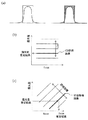
以下、本発明の第1の実施形態による構造体の立体(断面)形状推定方法の詳細について説明する。以下では、図4の上段図(a)、中段図(b)及び下段図(c)に示す断面プロファイルを有する3種類の試料A、B及びCを解析対象とする。
(First embodiment)
Details of the solid (cross-sectional) shape estimation method of the structure according to the first embodiment of the present invention will be described below. In the following, three types of samples A, B, and C having cross-sectional profiles shown in the upper diagram (a), middle diagram (b), and lower diagram (c) of FIG.
まず、CD-SEMにより、前記3種類の断面プロファイルを有する構造体の上面観察画像を取得し、上記構造体のエッジ部を解析領域に指定する。対象エッジには、設計上の直線部分を選択し、上記直線に沿った方向をy方向とする。 First, an upper surface observation image of the structure having the three types of cross-sectional profiles is acquired by CD-SEM, and an edge portion of the structure is designated as an analysis region. For the target edge, a designed straight line portion is selected, and the direction along the straight line is defined as the y direction.
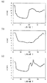
次に、エッジ検出時のしきい値Tを様々に変えてエッジを検出し、Tの関数としてエッジ点列 {xi(T)} (ただし、i=1,2, ,n)を求め、上記点列の平均エッジ位置<x(T)>からの偏差σ2 (T) = Σ[xi(T)-<x(T)>]2 を計算した。次に、σ(T)をしきい値Tに対してプロットすると、図5の上段図(a)、中段図(b)及び下段図(c)が得られる。前述したように、各段に示す点列は、図4の同じ段の断面プロファイルを有する構造体に対応する。 Next, an edge is detected by changing the threshold value T at the time of edge detection, and an edge point sequence {xi (T)} (where i = 1, 2,, n) is obtained as a function of T. The deviation σ 2 (T) = Σ [xi (T) − <x (T)>] 2 from the average edge position <x (T)> of the point sequence was calculated. Next, when σ (T) is plotted against the threshold value T, an upper diagram (a), a middle diagram (b), and a lower diagram (c) in FIG. 5 are obtained. As described above, the point sequence shown in each stage corresponds to the structure having the cross-sectional profile of the same stage in FIG.
一般に、検出信号強度のx方向分布I(x)は、構造体のエッジ近傍にピークをもつ。例えばレジストラインパターン等、ある幅Wで凸構造をもついわゆるラインパターンを観察すると、図4に示す各パターンの左右エッジの各々に対応して2つの強度ピークが現れる。つまり、片方のエッジを観察すると、同じしきい値Tに対して検出信号強度の分布ピークの両側に2つのエッジ検出点が得られる。よって、σ(T)は、上記ピークの構造体の内側と外側の各々に対して別々に求める。 In general, the x-direction distribution I (x) of the detection signal intensity has a peak near the edge of the structure. For example, when a so-called line pattern having a convex structure with a certain width W, such as a resist line pattern, is observed, two intensity peaks appear corresponding to the left and right edges of each pattern shown in FIG. That is, when one edge is observed, two edge detection points are obtained on both sides of the distribution peak of the detection signal intensity with respect to the same threshold value T. Therefore, σ (T) is obtained separately for each of the inside and outside of the peak structure.
一般に、構造体の外側(スペース側)では、外側から強度が徐々に増大して所定のしきい値に達した点のx座標をエッジ位置とする。一方、構造体の内側(ライン側)では、内側から強度が徐々に増大して所定のしきい値に達した点のx座標をエッジ位置とし、これらの値からσ(T)を求める。なお、パターン幅Wが極端に小さくなると、左右のエッジに対する上記ピークが重なり、1本のラインパターンに対して1個のピークが観察されるようになる。この場合、しきい値とx座標は1対1に対応する。 In general, on the outside (space side) of the structure, the x coordinate of the point where the intensity gradually increases from the outside and reaches a predetermined threshold value is set as the edge position. On the other hand, on the inner side (line side) of the structure, the x coordinate of the point where the intensity gradually increases from the inner side and reaches a predetermined threshold is set as the edge position, and σ (T) is obtained from these values. When the pattern width W becomes extremely small, the above peaks for the left and right edges overlap, and one peak is observed for one line pattern. In this case, the threshold value and the x coordinate correspond to each other one to one.
次に、解析領域内で、検出信号強度の分布I(x)のy方向の平均分布<I>(x)を求め、各しきい値Tを、検出信号強度が<I>(x)=Tとなる特定のx座標に対応させる。これにより、しきい値Tの関数としての偏差σ(T)を、xの関数としての偏差σ(x)に変換する。このとき、上記ピークの構造体の外側/内側のxに対する偏差σ(T)は、各々の構造体の外側/内側のxに対応させる。偏差σ(x)を検出信号強度分布<I>(x)とともにプロットすると、図6に示す特性図となる。図6の上段図(a)、中段図(b)及び下段図(c)に示す特性図は、いずれも図4の同じ段の断面プロファイルを有する構造体に対応する。図6の各図は、位置xに入射した電子線に対して得られる平均的なエッジ位置における検出エッジ変動を表わす。 Next, in the analysis region, an average distribution <I> (x) in the y direction of the distribution I (x) of the detection signal intensity is obtained, and each threshold value T is set to <I> (x) = Corresponds to a specific x coordinate of T. Thus, the deviation σ (T) as a function of the threshold value T is converted into a deviation σ (x) as a function of x. At this time, the deviation σ (T) of the peak with respect to the outside / inside x of the structure is made to correspond to the outside / inside x of each structure. When the deviation σ (x) is plotted together with the detection signal intensity distribution <I> (x), the characteristic diagram shown in FIG. 6 is obtained. The characteristic diagrams shown in the upper diagram (a), the middle diagram (b), and the lower diagram (c) of FIG. 6 all correspond to the structures having the same cross-sectional profile of FIG. Each figure of FIG. 6 represents the detected edge fluctuation at the average edge position obtained for the electron beam incident on the position x.
膜減りが大きく、かつ、順テーパ形状を有する試料Aの場合(図4の上段図(a))、偏差σ(x)は構造体の外側下部の平坦面で大きく、入射電子線がエッジに近づくと急激に減少して最小値となり、その後、構造体の中心に向けて徐々に増大し、構造体の上部の平坦面近傍で極大をとる。 In the case of the sample A having a large film thickness and a forward tapered shape (the upper diagram (a) in FIG. 4), the deviation σ (x) is large on the flat surface at the outer lower part of the structure, and the incident electron beam is at the edge. When approaching, it rapidly decreases and reaches a minimum value, then gradually increases toward the center of the structure, and reaches a maximum near the flat surface at the top of the structure.
一方、ほぼ垂直又はやや逆テーパ形状の側壁を有し、かつ、膜減りが少ない試料B(図4の中段図(b))、試料C(図4の下段図(c))では、偏差σ(x)は、最小値を取った後、急激に増大して台地状のピークを取り、いったん減少した後、構造体の中心に向けて徐々に増大し、構造体の上部の平坦面近傍で極大となる。上記ピークの高さは、逆テーパ状側壁をもつ試料Cの方がやや大きい。
このような分布形状の差異は、断面プロファイルの違いを反映したものと考えられる。
On the other hand, in the sample B (middle diagram (b) in FIG. 4) and the sample C (lower diagram (c) in FIG. 4) having a substantially vertical or slightly inverted side wall and little film loss, the deviation σ (x) takes a minimum value, then increases rapidly to take a plateau-like peak, decreases once, gradually increases toward the center of the structure, and near the flat surface at the top of the structure. It becomes maximum. The height of the peak is slightly larger in the sample C having the reverse tapered side wall.
Such a difference in distribution shape is considered to reflect a difference in cross-sectional profile.
次に、偏差σ(x)の形状のもつ意味について説明する。
まず、解析領域内部において、平均検出信号強度分布<I>(x)に対応して、便宜的に平均断面プロファイル<Z>(x)を考え、実際の構造体の3次元形状Z(x,y)を次式で表わす。
Next, the meaning of the shape of the deviation σ (x) will be described.
First, in the analysis region, the average cross-sectional profile <Z> (x) is considered for convenience, corresponding to the average detection signal intensity distribution <I> (x), and the three-dimensional shape Z (x, y) is expressed by the following equation.
![]()
![]()
すなわち、実際の3次元形状Z(x,y)は、平均断面プロファイル<Z>(x)をエッジ点位置yに応じてx方向にΔx(y)シフトし、さらに断面プロファイルに変動ΔZ(x,y)を与えたものと考える。ここで、Δx(y)は、各y毎に、例えば|ΔZ(x,y)|のx方向積分値が最小になるように決める。 That is, the actual three-dimensional shape Z (x, y) shifts the average cross-sectional profile <Z> (x) by Δx (y) in the x direction according to the edge point position y, and further changes the cross-sectional profile by ΔZ (x , y). Here, Δx (y) is determined for each y so that, for example, | ΔZ (x, y) |
次に、上記表現に対応して、実際に観察される検出信号強度の3次元分布も、次のように表わすことができる。
![]()
![]()
ここで、ΔI(x, y)は、ΔZ(x,y)に対応して断面プロファイルの平均からのずれによって生じる項である。Δnoise(x,y)は、実際の検出画像に重畳するランダムな検出ノイズであり、その振幅は位置・画像に依らない。Δx(y)は、各y毎に、例えば|ΔI(x,y)|2のx方向のエッジ近傍における積分値が最小になるように決める。 Here, ΔI (x, y) is a term generated by a deviation from the average of the cross-sectional profile corresponding to ΔZ (x, y). Δnoise (x, y) is a random detection noise superimposed on an actual detection image, and its amplitude does not depend on the position / image. Δx (y) is determined for each y so that, for example, | ΔI (x, y) | 2 near the edge in the x direction is minimized.
さらに、上記表現に対応して、検出されるエッジ点列の平均からの偏差σ(x)も、上記各項に起因する成分に分割することができる。
![]()
![]()
ここで、σ_measuredは計測結果である。σ_yは、各y毎に、その断面を平均断面プロファイルで最適フィットしたときの構造体のエッジ位置のバラツキに起因する成分である。σ_xzは、構造体の断面形状の変化に起因する成分である。σ_noiseは、検出(画像)ノイズに起因するエッジ検出誤差に起因する成分である。 Here, σ_measured is a measurement result. σ_y is a component due to variations in the edge position of the structure when the cross section is optimally fitted with an average cross section profile for each y. σ_xz is a component resulting from a change in the cross-sectional shape of the structure. σ_noise is a component caused by an edge detection error caused by detection (image) noise.
(エッジ変動成分の分解方法の詳細)
次に、計測されたエッジ変動値σ_measuredを、上述した4つの成分に分解する方法について説明する。以下、各成分について説明する。
(Details of edge fluctuation component decomposition method)
Next, a method for decomposing the measured edge fluctuation value σ_measured into the above-described four components will be described. Hereinafter, each component will be described.
構造体のエッジ位置のy方向の変動は、一般に、その空間周波数特性が1/f特性に従うのに対し、表面凹凸に起因する計測ばらつき及び検出ノイズは、その空間周波数特性がランダムであると考えられる。そこで、σ_yは、y方向の空間周波数fに対して1/f特性を有する成分(便宜上「真のLER」と呼ぶ)と考える。 In general, the fluctuation of the edge position of the structure in the y direction has a spatial frequency characteristic that follows the 1 / f characteristic, whereas the measurement variation and detection noise caused by surface irregularities are considered to have random spatial frequency characteristics. It is done. Therefore, σ_y is considered as a component having a 1 / f characteristic with respect to the spatial frequency f in the y direction (referred to as “true LER” for convenience).
なお、エッジに沿って測定されたx方向のエッジ点検出位置のばらつきを、1/f特性を有する成分と、それ以外の成分に分解する方法については、特許文献1に説明されている。ここで、LER成分の分解は、各しきい値毎に行ってもよいし、又は、ある代表的なしきい値Tに対して行ってもよい。
Note that
真のLERは、構造体のエッジ位置自体のy方向の変動である。よって、しきい値Tを変えて求めた計測結果に対してはほぼ共通と考えることができる。このため、後者の考えも合理的である。 The true LER is a variation in the y direction of the edge position of the structure itself. Therefore, it can be considered that the measurement results obtained by changing the threshold T are almost common. For this reason, the latter idea is also reasonable.
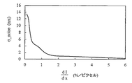
σ_noiseは、信号強度分布の傾斜に依存する。平滑平坦面に対して得られた画像に、1次元(x)方向に強度勾配を加え、平均レベルのしきい値に対して得られたエッジ点の変動を求めた結果を図7に示す。図7に示すように、検出信号の強度勾配が増えると、σ_noiseは小さくなる。σ_noise(x)は、平均検出強度分布の位置xにおける勾配に対するσ_noiseを図7から求めることにより計算することができる。 σ_noise depends on the slope of the signal intensity distribution. FIG. 7 shows the result obtained by adding the intensity gradient in the one-dimensional (x) direction to the image obtained on the smooth flat surface and obtaining the fluctuation of the edge point obtained with respect to the average level threshold value. As shown in FIG. 7, as the intensity gradient of the detection signal increases, σ_noise decreases. σ_noise (x) can be calculated by obtaining σ_noise with respect to the gradient at the position x of the average detected intensity distribution from FIG.
計測結果σ_measuredから、σ_y及びσ_noiseの寄与を除くと、σ_xzを求めることができる。
ここで、図4の上段図(a)、中段図(b)及び下段図(c)に示すような断面プロファイルを有する試料A、B及びCに対してσ_y及びσ_noiseを計算し、想定結果σ_measuredを、σ_y、σ_noise、σ_xzに分解した結果を図8の上段図(a)、中段図(b)及び下段図(c)に示す。図8から分かるように、断面プロファイルが逆テーパ形状である場合、σ_xzに顕著なピークが現れる。
If the contribution of σ_y and σ_noise is removed from the measurement result σ_measured, σ_xz can be obtained.
Here, σ_y and σ_noise are calculated for samples A, B, and C having cross-sectional profiles as shown in the upper diagram (a), middle diagram (b), and lower diagram (c) of FIG. 8 are shown in the upper diagram (a), the middle diagram (b), and the lower diagram (c) of FIG. As can be seen from FIG. 8, when the cross-sectional profile is an inversely tapered shape, a significant peak appears in σ_xz.
以下では、顕著なピークが発生する原因を考察するために、表面の凹凸が検出信号強度分布に及ぼす影響を次の2つに分類する。 In the following, in order to consider the cause of the occurrence of a prominent peak, the influence of surface irregularities on the detection signal intensity distribution is classified into the following two.
[分類1]
この分類では、電子線は、最初に順テーパ面に入射すると考える。このとき、構造体内部で散乱された後、再び構造体外に出て検出される電子の数は、順テーパ面上の入射位置のごく近傍の凹凸パターンの影響を受けると考えられる。
[Category 1]
In this classification, the electron beam is considered to be incident on the forward tapered surface first. At this time, the number of electrons that are scattered inside the structure and then go out of the structure again and are detected is considered to be affected by the uneven pattern in the vicinity of the incident position on the forward tapered surface.
[分類2]
この分類では、電子線は、エッジ点から離れた構造体上部における比較的平坦な面に入射すると考える。このとき、構造体内部で散乱された電子の一部が構造体の側面又は逆テーパ面から構造体の外部へ抜け出し、検出される。このとき、外部に抜け出す電子は、側面の凹凸パターンの影響を受ける。このように入射面とは異なる面から外部に抜け出す電子は、その絶対数が少ない。しかし、表面散乱により検出される電子数も比較的少ないので、側面の凹凸パターンの影響を受けた電子が順テーパ面に対する検出結果に及ぼす影響は無視できないと考えられる。
[Category 2]
In this classification, the electron beam is considered to be incident on a relatively flat surface at the top of the structure away from the edge point. At this time, a part of the electrons scattered inside the structure escapes from the side surface or reverse tapered surface of the structure to the outside of the structure and is detected. At this time, electrons that escape to the outside are affected by the uneven pattern on the side surface. Thus, the absolute number of electrons that escape to the outside from a surface different from the incident surface is small. However, since the number of electrons detected by surface scattering is relatively small, it is considered that the influence of the electrons affected by the uneven pattern on the side surface on the detection result for the forward tapered surface cannot be ignored.
この影響は、構造体内部の電子線進入長の範囲で、垂直又は逆テーパ面の面積に依存し、垂直又は逆テーパ面高さが大きいほど大きい。また、その影響は、構造体のエッジから内部寄りの比較的広い領域に入射した電子線に及ぶ。 This influence is dependent on the area of the vertical or reverse tapered surface within the range of the electron beam penetration length inside the structure, and is greater as the vertical or reverse tapered surface height is larger. In addition, the influence extends to an electron beam incident on a relatively wide area closer to the inside from the edge of the structure.
図8の上段図(a)、中段図(b)及び下段図(c)に見られるσ_xzのピークは、垂直又は逆テーパの側面を有する構造体において、電子線が構造体の上部平坦面に入射した場合に見られる。このことから、構造体の上部平坦面に出現するσ_xzのピークは、分類2に起因すると考えられる。
The peak of σ_xz seen in the upper diagram (a), the middle diagram (b) and the lower diagram (c) of FIG. 8 indicates that the electron beam is on the upper flat surface of the structure in a structure having a vertical or reverse tapered side surface. Seen when incident. From this, the peak of σ_xz that appears on the upper flat surface of the structure is considered to be due to
そこで、σ_xzを、以下の2つの成分に分解した(式4)で表す
(1)電子線入射点近傍の順テーパ面上の凹凸パターンの影響
:σ_xz_near
(2)電子線入射点から比較的離れた略垂直又は逆テーパ面上の凹凸パターンの影響
:σ_xz_far
Therefore, σ_xz is represented by the following two components (formula 4)
(1) Influence of uneven pattern on the forward tapered surface near the electron beam incident point: σ_xz_near
(2) Influence of uneven pattern on a substantially vertical or reverse tapered surface relatively far from the electron beam incident point: σ_xz_far
![]()
![]()
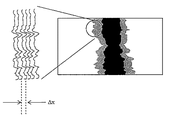
以下、上記(1)及び(2)の成分の詳細についてさらに説明する。
まず、凹凸パターンを有する順テーパ面に入射した電子線の散乱に及ぼす凹凸の影響(上記(1)の成分)について考える。ある一定角度の傾斜面に正弦波状の凹凸が存在し、凹部又は凸部の中心(図9の上段図(a)の点P)にビームが入射したとする。ビームの入射位置に対して凹凸の位相を180度変化させると、検出位置が、位相の±方向に1周期分変動する。例えば、ビームが凹部の中心に入射した場合、検出位置は位相の+方向に最大のずれが生じ、ビームが凸部の中心に入射した場合、検出位置は位相の−方向に最大のずれが生じる。
Hereinafter, the details of the components (1) and (2) will be further described.
First, the influence of the unevenness (component (1) above) on the scattering of the electron beam incident on the forward tapered surface having the uneven pattern will be considered. It is assumed that sinusoidal irregularities exist on an inclined surface at a certain angle, and the beam is incident on the center of the concave portion or convex portion (point P in the upper diagram (a) of FIG. 9). When the uneven phase is changed by 180 degrees with respect to the incident position of the beam, the detection position changes by one cycle in the ± direction of the phase. For example, when the beam is incident on the center of the concave portion, the detection position has a maximum deviation in the positive direction of the phase, and when the beam is incident on the center of the convex portion, the detection position has the largest deviation in the negative direction of the phase. .
以下では、説明を簡単にするため、図9の上段図(a)に示すように、平均的な傾斜角θが一定であり、かつ、その表面に沿って凹凸パターンをもつ側壁形状を有する構造体の平均側壁面上の点Pを考える。点P上に代表周期Lの表面凹凸の凸部中心が存在する場合、電子が点Pに向かって入射したとき、検出される信号強度の増加分が最大となり、エッジ検出位置のシフト量が−方向に最大となるとする。逆に、点P上に表面凹凸の凹部中心が存在する場合、検出される信号強度の減少分が最大となり、エッジ検出位置のシフト量が+方向に最大となるとする。 In the following, for the sake of simplicity, as shown in the upper diagram (a) of FIG. 9, a structure having a sidewall shape having a constant average inclination angle θ and having an uneven pattern along the surface thereof. Consider a point P on the average side wall surface of the body. When the convexity center of the surface irregularity having the representative period L exists on the point P, when electrons are incident toward the point P, the increase in the detected signal intensity is maximized, and the shift amount of the edge detection position is − Suppose the maximum in the direction. On the contrary, when the concave and convex center of the surface irregularity exists on the point P, the detected signal intensity decrease is maximized, and the shift amount of the edge detection position is maximized in the + direction.
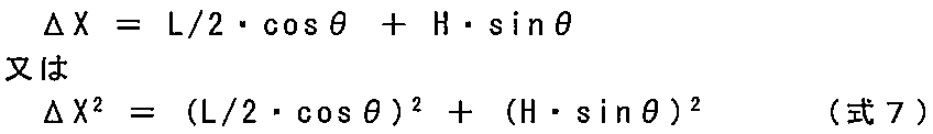
このとき、凹凸によるエッジの検出位置のシフト量は、凸部中心のx座標位置により決まり、その変動振幅Δxは、上記2つのケースにおける凸部中心間のx方向距離となる。従って、側壁面上の凹凸周期をLとし(すなわち、上記x方向の距離はL/2であり)、検出位置が図9の中段図(b)で決まるとすると、エッジの検出位置の変動幅ΔXは、凹凸周期L、側壁傾斜面の角度(傾斜角)θにより、次式のように推定することができる。 At this time, the shift amount of the edge detection position due to the unevenness is determined by the x coordinate position of the center of the convex portion, and the fluctuation amplitude Δx is the x-direction distance between the convex portion centers in the two cases. Accordingly, assuming that the concave-convex period on the side wall surface is L (that is, the distance in the x direction is L / 2) and the detection position is determined by the middle diagram (b) of FIG. ΔX can be estimated by the following equation using the uneven period L and the angle (tilt angle) θ of the side wall inclined surface.
![]()
![]()
これに対し、検出位置が図9の下段図(c)で決まるとすると、エッジの検出位置の変動幅ΔXは、高さH、側壁傾斜面の角度(傾斜角)θにより、次式のように推定することができる。 On the other hand, if the detection position is determined by the lower diagram (c) of FIG. 9, the fluctuation range ΔX of the edge detection position is expressed by the following equation depending on the height H and the angle (inclination angle) θ of the side wall inclined surface. Can be estimated.
![]()
![]()
一般に、傾斜角θが比較的小さい領域では式5が支配的となり、傾斜角θが比較的大きい領域では式6が支配的となる。実際には、傾斜角θは、側面の凹凸周期と高さの両方に依存すると考えられる。従って、両式を加算した次式により、エッジ検出位置の変動幅ΔXを推定することも可能である。
In general,
さらに、エッジ検出位置の変動幅ΔXと傾斜面の傾斜角θとの関係は、表面凹凸による電子線信号の強度変動量が表面に対する電子線の入射角に依存するという特性を用いて求めることもできる。 Further, the relationship between the variation width ΔX of the edge detection position and the inclination angle θ of the inclined surface can be obtained by using the characteristic that the intensity fluctuation amount of the electron beam signal due to the surface unevenness depends on the incident angle of the electron beam to the surface. it can.
例えば表面に適当な周期L又は高さHの凹凸を有する平面(図10の上段図(a1))に、様々な入射角度の電子線を照射・走査したときの検出信号強度分布をシミュレーションにより計算する(図10の上段図(a2))。このとき、検出強度の変動幅ΔIは、入射角θの関数となる(図10の中段図(b))。 For example, the detection signal intensity distribution is calculated by simulation when an electron beam with various incident angles is irradiated and scanned on a flat surface (upper figure (a1) in FIG. 10) having irregularities with an appropriate period L or height H on the surface. (Upper diagram (a2) in FIG. 10). At this time, the fluctuation range ΔI of the detected intensity is a function of the incident angle θ (middle diagram (b) in FIG. 10).
一方、強度変動幅ΔI(θ)と、エッジ検出位置の変動幅ΔXと、平均信号強度分布I(x)の関係は、図10の下段図(c)に示すように、次式で表すことができる。 On the other hand, the relationship between the intensity fluctuation range ΔI (θ), the edge detection position fluctuation range ΔX, and the average signal intensity distribution I (x) is expressed by the following equation as shown in the lower diagram (c) of FIG. Can do.
![]()
![]()
ただし、式8は、検出信号の強度分布のピークにおいて勾配が0(zero)になると、値が発散する。このため、式8は、検出信号の強度分布のピークにおいて勾配が0(zero)の場合には用いることが出来ないことに注意が必要である。実際には、エッジシフト量の振幅ΔXは、側壁表面凹凸によるエッジ検出位置の計測ばらつきから推定される統計量であり、σ_xz_nearがこれに相当する。また、側壁表面の凹凸パターンはランダム量であるので、その周期L及び高さHに関しても統計的な代表値を用いる。例えば便宜上、平坦面の傾斜角θが0(zero)となるように選んでもよい。
However, the value of
次に、上記(2)の成分(ビームの入射位置から離れた表面位置の凹凸パターンの影響)について説明する。
平均的な側壁面に対し、図11の上段図(a)のQ点に電子線が入射したときの検出強度をIQとする場合に、同図内の曲線A及びBに示すように側壁面のパターンが変動した場合を考える。このとき、図11の下段図(b)に示すように、検出強度は検出強度IQに対してΔIA及びΔIBだけ変化し、検出エッジはそれぞれΔxA、ΔxBだけずれる。
Next, the component (2) (influence of the uneven pattern at the surface position away from the incident position of the beam) will be described.
When the detection intensity when the electron beam is incident on the point Q in the upper diagram (a) of FIG. 11 is IQ with respect to the average side wall surface, the side wall surface as shown by curves A and B in FIG. Consider the case where the pattern of fluctuates. At this time, as shown in the lower diagram (b) of FIG. 11, the detected intensity changes by ΔIA and ΔIB with respect to the detected intensity IQ, and the detected edges are shifted by Δx A and Δx B , respectively.
このとき、側壁面の大きさに対して電子線の広がりが同程度であるとすると、検出エッジに出現するずれ量ΔxA及びΔxBは、入射位置(Q点)に依らず、ほぼ一定と考えることができる。 At this time, assuming that the spread of the electron beam is about the same as the size of the side wall surface, the shift amounts Δx A and Δx B appearing at the detection edge are almost constant regardless of the incident position (Q point). Can think.
そこで、電子線の入射位置が、構造体のエッジ位置から構造体中の散乱電子が側壁に及ぶ範囲の間では、前述した(2)の影響がほぼ一定であると仮定し、σ_xz_far に対して台形状の分布形状として近似する。 Therefore, assuming that the incident position of the electron beam is in the range where the scattered electrons in the structure reach the side wall from the edge position of the structure, the effect of (2) described above is assumed to be almost constant, and σ_xz_far Approximate as a trapezoidal distribution shape.
台形の高さは、側壁の高さと角度に依存するが、例えば式4に従って、σ_xzの最小値から構造体側において、σ_xzからσ_xz_farを引いた後のσ_xz_nearの分布が、0(zero)からほぼ線形に増大するような高さに設定することが考えられる。図4の上段図(a)、中段図(b)及び下段図(c)に対応する各試料について、σ_xzを上記2つの成分に分解した結果を図12の上段図(a)、中段図(b)及び下段図(c)に示す。
The height of the trapezoid depends on the height and angle of the side wall, but for example, according to
(断面形状の推定方法)
次に、不確かさを表す偏差σを分解した結果から、構造体の断面形状を推定する方法について説明する。
(Section shape estimation method)
Next, a method for estimating the cross-sectional shape of the structure from the result of decomposing the deviation σ representing uncertainty will be described.
実際の構造体の断面形状は、丸みを帯びていたり、裾を引いていたり、様々な形状を有するものと考えられる。つまり、一般的に、側壁角θは、構造体の高さ方向又はx方向の位置に対して一定ではない。本実施形態に係る手法を用いれば、このような構造体であっても、その断面形状を適切に推定することができる。 The actual cross-sectional shape of the structure is considered to have various shapes such as a rounded shape, a skirted shape, and the like. That is, generally, the side wall angle θ is not constant with respect to the height direction of the structure or the position in the x direction. If the method according to the present embodiment is used, the cross-sectional shape of such a structure can be estimated appropriately.
以下、解析的形状推定法とモデルベースによる形状推定法の2つのアプローチによる断面推定法について説明する。
(解析的推定法)
解析的推定法では、しきい値又はx方向の位置に対し、式5、式6、式7、式8等を用いて、構造体の対応する高さにおける構造体表面の局所的な角度を求め、これをx方向に積分することにより構造体の断面形状を求める。すなわち、次式により、断面形状を求める。ただし、次式において積分範囲は0(zero)からxまでである。
Hereinafter, the cross-sectional estimation method based on the two approaches of the analytical shape estimation method and the model-based shape estimation method will be described.
(Analytical estimation method)
In the analytical estimation method, the local angle of the structure surface at the corresponding height of the structure is calculated by using
![]()
![]()
ここでは、式5と式8を用い、図12のσ_xz_nearより推定したθ(x)の分布と、推定される断面形状Z(x)を図13の上段図(a)、中段図(b)及び下段図(c)にそれぞれ示す。推定された断面形状(実線で示す形状)は、別途、断面観察より得られた形状(図4の上段図(a)、中段図(b)、下段図(c)の形状)とよく一致していることが分かる。
Here, using
一方、モデルベースによる形状推定法では、様々な断面形状に対して、その表面の凹凸(例えばその位相)を変化させたときの検出信号強度の分布を求め、各々に対して検出されるエッジ位置間のバラツキ(不確かさ)を、しきい値又はx方向の位置の関数として予め求めておく。次に、このバラツキ(不確かさ)と実際の測定結果とをマッチングさせ、最も近い断面形状を求める又は内挿・外挿により断面形状を推定する。 On the other hand, in the model-based shape estimation method, the distribution of detected signal intensity when the surface irregularities (for example, the phase) are changed for various cross-sectional shapes, and the edge positions detected for each are obtained. A variation (uncertainty) between them is obtained in advance as a function of a threshold value or a position in the x direction. Next, this variation (uncertainty) is matched with an actual measurement result, and the closest cross-sectional shape is obtained or the cross-sectional shape is estimated by interpolation / extrapolation.
検出信号の強度分布自体の計算結果ライブラリと計測結果とのマッチングを求めることにより断面形状を推定する従来のMBL法は、測定結果が検出系や検出強度変動に影響を受けるという課題があるのに対し、本方法は、これらの影響を受け難い。もっとも、本方法と従来のMBL法とを併用することもできる。また、マッチングには最尤法等を用いてもよい。 The conventional MBL method that estimates the cross-sectional shape by finding the matching between the calculation result library of the detection signal intensity distribution itself and the measurement result has the problem that the measurement result is affected by the detection system and detection intensity fluctuation In contrast, the method is less susceptible to these effects. However, the present method and the conventional MBL method can be used in combination. Further, a maximum likelihood method or the like may be used for matching.
(構造体立体形状推定処理手順)
図14に、第1の実施形態に対応する、構造体の立体形状を推定するための方法のフローチャートを示す。なお、後述する一連の処理は、計算機で実行されるプログラムに基づいて実現される。
(Structure solid shape estimation processing procedure)
FIG. 14 shows a flowchart of a method for estimating the three-dimensional shape of the structure corresponding to the first embodiment. Note that a series of processes described later is realized based on a program executed by a computer.
まず、電子顕微鏡により2次元画像を取得し、解析領域を指定する(ステップ1401)。この後、指定された解析領域における平均的な信号強度分布I(x)を算出する(ステップ1402)。信号強度は、指定範囲における最大強度で規格化する。この際、上記範囲における平均的なエッジ方向がy方向となるように画像を調整することが望ましい。 First, a two-dimensional image is acquired with an electron microscope, and an analysis region is designated (step 1401). Thereafter, an average signal intensity distribution I (x) in the designated analysis region is calculated (step 1402). The signal strength is normalized by the maximum strength in the specified range. At this time, it is desirable to adjust the image so that the average edge direction in the above range is the y direction.
次に、しきい値を指定の最小値から最大値まで所定の間隔毎(例えば5%から100%まで5%毎)に設定し、各しきい値毎にパターンエッジを検出し、しきい値Tの関数としてLERを求める(ステップS1403〜1408)。ここでは、T=I(x)の関係を用いてLERをxの関数に変換した後、これを各成分に分解する。さらに、式5、式6、式7、式8等に従って側壁角度θを求め(ステップS1409、1410)、側壁角度θをx方向に積分して断面形状を得る(ステップS1411)。ここまでの説明では、構造体の表面の凹凸パターンは、表面において等方的であると仮定した。局所的なレジストの溶解性ばらつき等に由来する凹凸に関しては、上記の仮定は、ほぼ正しい。一方、この仮定が成り立たないケースについては、後述する実施例5に述べる。
Next, a threshold value is set at a predetermined interval from a specified minimum value to a maximum value (for example, every 5% from 5% to 100%), and a pattern edge is detected for each threshold value. LER is obtained as a function of T (steps S1403 to 1408). Here, LER is converted into a function of x using the relationship of T = I (x), and then decomposed into each component. Further, the side wall angle θ is obtained according to
[実施例1]
本実施例では、前述した推定手法をCD-SEMに適用した実施例について説明する。
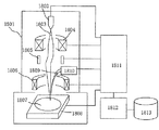
(装置構成)
図15に、本実施例で用いたCD-SEMのハードウェア構成の模式図を示す。本実施例のCD-SEMは、主として電子光学カラム(SEMカラム)と試料室からなる走査型電子線顕微鏡の筐体1801と、走査型電子線顕微鏡の制御系1811と、情報処理装置1812により構成される。
[Example 1]
In the present embodiment, an embodiment in which the above-described estimation method is applied to a CD-SEM will be described.
(Device configuration)
FIG. 15 shows a schematic diagram of the hardware configuration of the CD-SEM used in this example. The CD-SEM of this embodiment is mainly composed of a scanning electron
情報処理装置1812には、得られた走査電子画像や解析に必要なCADデータなどを格納するデータ記憶装置1813が接続されている。もっとも、データ記憶装置1813は、情報処理装置1812内に格納されていても良い。図示されてはいないが、情報処理装置1812は、CD-SEMの操作者がデータ処理のために必要な情報を装置に対して入力するための情報入力端末及び取得される走査電子画像を表示するための画像表示手段を備えている。情報入力端末の具体例には、キーボード、マウス、画像表示手段上に表示されるGUI画面等がある。
The
電子光学カラムは、電子銃1802、収束レンズ1804、偏向器1805、対物レンズ1806、検出器1810などにより構成される。試料室は、被検査対象である観察ウエハ1807を載置するステージ1808を備える。電子銃1802から観察ウエハ1807に対して照射される電子線1803により発生した二次電子1809は検出器1810によって検出され、制御系1811によってデジタルデータに変換された後、情報処理装置1812に転送され、解析に使用する画像データが生成される。
The electron optical column includes an
本実施例では、CD-SEMに備えられた走査電子顕微鏡を用いてパターン観察を行なって被検査対象の画像データを取得した。得られた画像データをデータ記憶装置1813に保存し、観察終了後、情報入力端末を操作して画像データ解析を実行し、ラフネス指標及び断面構造推定の解析を行った。解析処理は、情報処理装置1812が実行する。
In this example, pattern observation was performed using a scanning electron microscope provided in a CD-SEM, and image data to be inspected was acquired. The obtained image data was stored in the
(画像取得工程)
まず、制御系1811(情報処理装置1812)は、ArFレジストのラインパターンに対し、視野の左上から右下までの走査を32回行って得られた二次電子信号強度を平均化し、2次電子信号強度の2次元分布画像を取得する。必要に応じ、情報処理装置1812は、取得した画像をCD-SEMのモニタ画面上に表示する。ここで、観察画像の画素数は、縦・横方向に1500画素、1画素の1辺を1nm(ナノメートル)、視野内の観察画像の長さを縦横1.5μm(マイクロメートル)とする。
(Image acquisition process)
First, the control system 1811 (information processing apparatus 1812) averages the secondary electron signal intensity obtained by scanning the ArF resist line pattern 32 times from the upper left to the lower right of the field of view to obtain the secondary electrons. A two-dimensional distribution image of signal intensity is acquired. The
情報処理装置1812は、2次電子信号強度の2次元分布画像のうち解析したいエッジを含む領域に、それぞれ縦1024画素、横50画素の矩形形状の検査領域を設定する。また、エッジ抽出のためのしきい値Tの最小値Tmin、最大値Tmax、増分値ΔT、データ抽出のy方向のサンプリング間隔Δy、x方向のノイズ低減パラメータ、y方向の平均化パラメータS等、データ系列抽出に必要な情報を設定する。なお、データ抽出におけるy方向のサンプリング間隔ではなく、検出点数を設定することも可能である。これらの検査領域及びデータ系列抽出の条件は、例えばCD-SEMのGUI画面等を通じ、予め設定することが望ましい。
The
次いで、情報処理装置1812は、領域内のエッジラフネスのデータ系列を抽出するタスクを実行する。すなわち、情報処理装置1812は、設定された抽出開始点やサンプリング間隔に従って、検査領域内の画素データからサンプリング位置でのy座標に対応する信号強度分布を算出し、更に、最小値Tminから最大値Tmaxまで増分値ΔT毎に設定したしきい値Tに応じ、上記信号強度分布からエッジ点のx座標データを算出する。これらの処理を、設定されたサンプリング間隔に従って次々にy方向へ移動しながら実行し、最終的に、しきい値Tの関数として検査領域内でのエッジラフネスのデータ系列X(T)={Δxi(T)}={Δx1(T)、Δx2(T)、…}を取得する。
Next, the
具体的には、情報処理装置1812は、データ抽出開始点のy座標として、上記検査領域の下辺に対応するy座標を設定し、y方向のサンプリング間隔として1nm(ナノメートル)を設定し、検査領域内のエッジ点として1nm(ナノメートル)置きに1024個の点の位置(x1(T), y1(T)),…(xi(T), yi(T)),…(x1024(T), y1024(T))を抽出した。
Specifically, the
次に、情報処理装置1812は、抽出された点を以下の直線で近似し、フィッティングパラメータであるαとβの値を求めた。
![]()
![]()
次に、全てのしきい値Tに対するエッジ点の座標に対し、情報処理装置1812は、以下の式11に従ってエッジ点の上記直線からのずれ量Δxiを求め、エッジラフネス系列X(T)={Δxi}Tを生成する。
![]()
![]()
(画像処理工程)
次に、情報処理装置1812は、エッジラフネス系列X(T)={Δxi(T)}からしきい値毎にLERを求め、求めたLERを真のLERによる測定ばらつきσ_yと、表面凹凸による計測ばらつきσ_xzとに分解する。エッジラフネス系列から、真のLERによる測定ばらつきσ_yと表面凹凸による計測ばらつきσ_xzを求める方法については、例えば特許文献1に記載されている方法を用いることができるが、その代表的な手段について述べるならば以下の通りである。
(Image processing process)
Next, the
前述したように、測定されたLERには、パワースペクトル密度が空間周波数fの2乗に反比例する成分(真のLER)と、それ以外の高周波成分(ノイズ)とが重畳している。測定されたLERに平均化処理を施すと、後者の成分が減少する。このため、平均化処理の程度を表すパラメータ値を増やすのに伴い、高周波領域でのパワースペクトル密度分布がfの2乗に反比例するようになる。具体的には、異なるy座標におけるx方向の1次元信号強度分布を、y方向にS本平均化することを考えると、ランダムノイズの強度は、平均化によって1/Sに低減される。すなわち、平均化パラメータSの増加に伴って、パワースペクトル密度の周波数依存性が1/f2に近づいていく。このとき得られるパワースペクトルの密度が真のLERとなる。 As described above, a component (true LER) whose power spectral density is inversely proportional to the square of the spatial frequency f and other high-frequency components (noise) are superimposed on the measured LER. If the measured LER is averaged, the latter component is reduced. For this reason, as the parameter value representing the degree of the averaging process is increased, the power spectral density distribution in the high frequency region becomes inversely proportional to the square of f. Specifically, considering that one-dimensional signal intensity distributions in the x direction at different y coordinates are averaged in the y direction, the random noise intensity is reduced to 1 / S by averaging. That is, as the averaging parameter S increases, the frequency dependence of the power spectral density approaches 1 / f 2 . The density of the power spectrum obtained at this time becomes true LER.
ここで、平均化パラメータSで平均化処理されたデータから得られるラインエッジラフネス指標の値をσm(S)として、そのS依存性を次式にフィッティングする。
ただし、σm(1)は、平均化処理前のデータから求めたラインエッジラフネス計測値であり、Δyはエッジ点のy方向抽出間隔であり、Aはフィッティングパラメータである。S及びエッジ点の抽出間隔Δyは、2SΔy<1/f0 [nm(ナノメートル)]を満たすことが望ましい。ここで、f0は、通常のレジストパターンの場合、スペクトルの屈曲点において、0.008nm-1以下であることが多い。 Here, σm (1) is a line edge roughness measurement value obtained from the data before the averaging process, Δy is the y direction extraction interval of the edge points, and A is a fitting parameter. It is desirable that the extraction interval Δy between S and the edge point satisfies 2SΔy <1 / f 0 [nm (nanometer)]. Here, in the case of a normal resist pattern, f 0 is often 0.008 nm −1 or less at the inflection point of the spectrum.
ここでは、実験結果をよく説明するSの中で最も小さいSに対して求められたσ0=σを真のLERとした。この場合、空間周波数によらない計測ばらつき成分σbは、次式により求められる。 Here, σ 0 = σ obtained with respect to the smallest S among S that well explains the experimental results is defined as a true LER. In this case, the measurement variation component σb independent of the spatial frequency is obtained by the following equation.
![]()
![]()
さらに、情報処理装置1812は、測定されたLERから計測誤差σ_noiseを求め、これをσb(T)から取り除くことにより、側壁表面の凹凸パターンがxy平面に投影されることによる計測ばらつき(不確定性)を示すσ_xz(T)を求めた。
Further, the
![]()
![]()
ここで、構造体のしきい値Tに対応する高さにおける側壁角度θは、次式により求められる。 Here, the side wall angle θ at the height corresponding to the threshold value T of the structure is obtained by the following equation.
![]()
![]()
一方、y方向の計測範囲に対して、x方向の信号強度分布の平均<I>(x)を算出した。しきい値Tに対応するエッジ座標xは、x=<I>-1(T)より求めることができる。ただし、<I>-1は、<I>の逆関数である。 On the other hand, the average <I> (x) of the signal intensity distribution in the x direction was calculated for the measurement range in the y direction. The edge coordinate x corresponding to the threshold value T can be obtained from x = <I> −1 (T). However, <I> −1 is an inverse function of <I>.
ところで、構造体の断面形状z(=Z(x))は、前述したように、次式により求めることができる。 Incidentally, the cross-sectional shape z (= Z (x)) of the structure can be obtained by the following equation as described above.
![]()
![]()
このようにして求めた断面形状を、ウエハのパターン部を切断してSEMで観察した断面形状と比較を行ったところ、両者はよく一致することが確認された。また、AFMによる計測結果との比較も行ったが、こちらもよく一致することも確認された。 When the cross-sectional shape thus obtained was compared with the cross-sectional shape observed by SEM after cutting the pattern portion of the wafer, it was confirmed that they were in good agreement. In addition, a comparison with the measurement result by AFM was also made, and it was confirmed that this also coincided well.
なお、上の説明ではσsとσ_noiseは物理的な意味を持つ値として、各々独立に計測して求めるとしたが、これらの量はフィッティングパラメータとして考えてもよい。すなわち、他の方法により観察した断面形状と、本発明により推定した断面形状がよく一致するような、σsとσ_noiseを用いればよい。 In the above description, σs and σ_noise are obtained by measuring each independently as values having physical meanings, but these amounts may be considered as fitting parameters. That is, σs and σ_noise may be used so that the cross-sectional shape observed by another method and the cross-sectional shape estimated by the present invention are in good agreement.
[実施例2]
本実施例においては、1次元マスクパターンの断面構造だけでなく、2次元マスクパターンに対しても立体的構造を推定できる方法の一例を説明する。本実施例で用いる走査形電子顕微鏡の構成は、実施例1と同様なので説明を省略する。
[Example 2]
In this embodiment, an example of a method capable of estimating a three-dimensional structure not only for a cross-sectional structure of a one-dimensional mask pattern but also for a two-dimensional mask pattern will be described. Since the configuration of the scanning electron microscope used in the present embodiment is the same as that of the first embodiment, the description thereof is omitted.
実施例1の手法を2次元マスクパターンに拡張する方法には次の2つの方法が考えられる。
[第1の方法]
この方法では、実施例1の方法により1次元パターンに対してしきい値とパターン高さの関係を求め、この関係をそのまま2次元パターンに対して適用する。
The following two methods can be considered as a method of extending the method of the first embodiment to a two-dimensional mask pattern.
[First method]
In this method, the relationship between the threshold value and the pattern height is obtained for the one-dimensional pattern by the method of
[第2の方法]
この方法では、実施例1の方法を2次元エッジ情報に対して拡張する。
まず、第1の方法について説明する。情報処理装置1812は、実施例1の方法と同様に取得した2次元画像(図16の上段左図)に対し、その1次元パターン部分に実施例1の方法を適用して断面形状z=Z(x)を求める(推定する)。
[Second method]
In this method, the method of the first embodiment is extended to the two-dimensional edge information.
First, the first method will be described. The
次に、情報処理装置1812は、上記z=Z(x)と、上記形状の導出に用いた信号強度分布T=I(x)の2つの関係からxを消去することにより、構造体の高さzとしきい値Tの関係z=Z’(T)を得る。図16の上段左図の2次元マスクパターンに対するSEM観察画像に対し、しきい値Tを変えてエッジを抽出すると、図16の上段中図のような等高線が得られる。
Next, the
次に、情報処理装置1812は、上記構造体の高さzとしきい値Tの関係に従い、図16の上段中図のTをzに変換し、図16の上段右図のような2次元パターンの高さ情報を得る。なお、Tとzの間には、図16の下段に示す関係が成立する。この関係を与えるデータは、例えばデータ記憶装置1813に予め格納しておく。
Next, the
本方法の問題は、実施例1の方法により求めた構造体の高さzとしきい値Tの関係z=Z(T)が、2次元マスクパターンの構造体において成立する保証が必ずしもないことである。一般に、高さと信号強度の関係は一意的ではない。しかしながら、ライン幅等のパターン特性が近いパターンに対しては、本方法は、比較的よい近似を与えることができる。 The problem with this method is that there is no guarantee that the relationship z = Z (T) between the height z of the structure and the threshold value T obtained by the method of the first embodiment is satisfied in the structure of the two-dimensional mask pattern. is there. In general, the relationship between height and signal strength is not unique. However, for patterns with similar pattern characteristics such as line width, the method can provide a relatively good approximation.
次に、第2の方法について説明する。本方法は、同一のマスク上の異なる複数の位置に同一の設計パターンが存在する場合に適用することができる。まず、情報処理装置1812は、マスク上の複数の同一2次元パターンについて形成された、ウエハ上の複数の2次元パターンを同一条件でSEM観察し、複数のSEM画像(信号強度分布)を得る。
Next, the second method will be described. This method can be applied when the same design pattern exists at a plurality of different positions on the same mask. First, the
これら複数のSEM画像に対し、情報処理装置1812は、あるしきい値Tで切った時のエッジ座標列を求め、各座標点を結んだ等高線を考える。この際、計測精度を確保するため、エッジの抽出は、等高線に略垂直な方向に沿った信号強度分布を求め、これに対してしきい値を適用することにより求めることが望ましい。
For these SEM images, the
次に、情報処理装置1812は、上記複数の画像に対して求めた等高線間の距離偏差の総和が最小となるように、各画像を平行方向にシフトする。シフト位置の基準は、適宜設定してよい。さらに、情報処理装置1812は、平行シフト後の各画像の等高線に対して平均形状を求め、各画像の等高線に対して等高線の接線と垂直な方向に対する平均形状との差分(距離)を算出する。
Next, the
情報処理装置1812は、各エッジ点に対し、差分の分布の標準偏差を求め、これを実施例1におけるσb(T)に相当する値と仮定する。これにより、実施例1と同様、式5、式6、式7、式8等を用いて求めた傾斜角θを、当該位置におけるしきい値Tに対応する高さの側壁角度θとする。しきい値Tを変えてエッジを抽出した方向に沿って、式9と同様の積分を行うことにより、上記方向に沿った縦構造を求めることができる。
The
第2の方法で求めたσb(T)は、真のLERに相当する成分を含むことが懸念されるが、平行シフトを行うことにより、比較的長周期のLERに起因するエッジシフトは相殺することができると期待される。さらに、真のLERの短周期成分と計測誤算成分は、上記σb(T)から適宜除去することが望ましい。 There is a concern that σb (T) obtained by the second method includes a component corresponding to a true LER, but the edge shift caused by a relatively long period of LER cancels out by performing a parallel shift. Expected to be able to. Further, it is desirable that the true LER short period component and the measurement miscalculation component are appropriately removed from the σb (T).
本実施例の場合にも、実施例1の場合と同様に、σsとσeは、物理的な意味を持つ値として、各々独立に計測して求めても良いし、フィッティングパラメータとして考えても良い。発明者は、このような手法により推定した構造体の断面形状が、同じ構造体を切断してSEM画像として観察した断面形状とよく一致することを確認した。 Also in the present embodiment, as in the case of the first embodiment, σs and σe may be obtained by measuring each independently as values having physical meanings, or may be considered as fitting parameters. . The inventor has confirmed that the cross-sectional shape of the structure estimated by such a technique is in good agreement with the cross-sectional shape observed as an SEM image by cutting the same structure.
[実施例3]
本実施例では、本発明を、半導体集積回路等の製造に用いられる光リソグラフィによるレジストパターン形成プロセス、又はそれを用いて形成した半導体集積回路の立体的構造の品質評価、並びに上記プロセスモニターに適用する例について説明する。
[Example 3]
In this embodiment, the present invention is applied to a resist pattern formation process by photolithography used for manufacturing a semiconductor integrated circuit or the like, or a three-dimensional structure quality evaluation of a semiconductor integrated circuit formed using the resist pattern forming process, and the process monitor. An example will be described.
本実施例では、形成されたパターンの品質指標として、推定したパターンの高さと設計上のパターンの高さの偏差の絶対値を評価領域の全面について積分した値、又は、その値の2乗平均値を用いる(図17の上段図(a)の右図にハッチングで示す部分の面積に対応する量)。 In the present embodiment, as the quality index of the formed pattern, a value obtained by integrating the absolute value of the deviation between the estimated pattern height and the design pattern height over the entire evaluation area, or the root mean square of the values A value is used (amount corresponding to the area of the hatched portion in the right diagram of FIG. 17A).
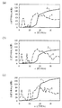
なお、より単純に、前述の実施例の手法を適用して推定した断面形状(例えば図17の上段図(a)の左図における曲線下部)の断面積Spと理想的設計形状(例えば図17の上段図(a)の左図における長方形部分)の断面積Siの比Sp/Si(1次元マスクパターンの場合)、又は、前述の実施例の手法により推定した形状の体積Vpと理想的設計形状の体積Viの比Vp/Vi(2次元マスクパターンの場合)を、パターン品質指標として用いても良い。ただし、この場合には、設計上のパターンが本来存在しないはずの領域に存在するパターンの面積又は体積を負の値で扱うことが好ましい。これにより、設計上のパターンが本来存在しないはずの領域にパターンが存在する場合にも、品質劣化として検知することができる。 Note that, more simply, the cross-sectional area Sp of the cross-sectional shape estimated by applying the method of the above-described embodiment (for example, the lower portion of the curve in the left diagram of FIG. 17A) and the ideal design shape (for example, FIG. 17). The ratio Sp / Si (in the case of a one-dimensional mask pattern) of the cross-sectional area Si of the upper part (a) in the left part of the upper diagram (a), or the volume Vp of the shape estimated by the method of the above-described embodiment and the ideal design The ratio Vp / Vi of the shape volume Vi (in the case of a two-dimensional mask pattern) may be used as a pattern quality index. However, in this case, it is preferable to treat the area or volume of the pattern existing in the region where the design pattern should not exist as a negative value. Thereby, even when a pattern exists in an area where a design pattern should not originally exist, it can be detected as quality degradation.
2次元マスクパターンに対する理想的な設計形状には、回路パターンの設計形状、上記回路設計形状に対して光学的近接効果補正等を施したマスクパターンに対する光学シミュレーションの結果、様々な実際の露光結果に対して前述の実施例で説明した手法を適用して推定した体積のうちの最大値等を用いることができる。 The ideal design shape for a two-dimensional mask pattern includes a circuit pattern design shape, optical simulation results for a mask pattern obtained by performing optical proximity effect correction on the circuit design shape, and various actual exposure results. On the other hand, the maximum value of the volume estimated by applying the method described in the above embodiment can be used.
パターン形成用露光装置のフォーカス及び露光量条件をウエハ上の露光ショット毎にマトリクス状に様々に変化させて露光したウエハに対し、上記露光ショット毎にマスク上の同一パターンに対するレジストパターンをCD-SEMで観察し、その観察像からショットごとにパターン寸法を測定すると共に、実施例1に記載した方法によりパターン断面形状を推定し、上記パターン品質指標を求めた。 For wafers exposed by changing the focus and exposure amount conditions of the pattern forming exposure apparatus in a matrix for each exposure shot on the wafer, the resist pattern for the same pattern on the mask is CD-SEM for each exposure shot. The pattern size was measured for each shot from the observed image, the pattern cross-sectional shape was estimated by the method described in Example 1, and the pattern quality index was obtained.
図17の中段図(b)に示すように、パターンの寸法は、露光量に対して単調減少したが、フォーカス設定値に対するパターン寸法変化は小さく、パターン寸法変化からフォーカス設定値を推定するのは難しかった。これに対して、図17の下段図(c)に示すように、パターン品質指標は、露光量及びフォーカスの両方の設定値に対してほぼ単調に変化し、フォーカス設定値のモニタとして適用できた。ただし、パターン品質指標は、露光量に対しても変化する。そこで、まずパターン寸法変化から露光量を推定し、上記露光量に対して、パターン品質指標を用いてフォーカス設定値を推定することが望ましい。 As shown in the middle diagram (b) of FIG. 17, the pattern dimension monotonously decreased with respect to the exposure amount, but the pattern dimension change with respect to the focus setting value is small, and the focus setting value is estimated from the pattern dimension change. was difficult. On the other hand, as shown in the lower diagram (c) of FIG. 17, the pattern quality index changes almost monotonously with respect to both the exposure amount and the set value of the focus, and can be applied as a monitor of the focus set value. . However, the pattern quality index also changes with respect to the exposure amount. Therefore, it is desirable to first estimate the exposure amount from the pattern dimension change, and estimate the focus setting value for the exposure amount using a pattern quality index.
本実施例のように、推定された断面形状を、形成されたパターンの品質指標に用いれば、簡便かつ高速に最適な製造条件を判定したり、品質低下を検知することができる。また、当該判定結果等を製造プロセスにフィードバックすれば、形成されるパターンの品質劣化を抑制し、半導体装置をはじめとする各種素子の性能を向上させることができる。 If the estimated cross-sectional shape is used as a quality index of the formed pattern as in the present embodiment, it is possible to determine optimum manufacturing conditions simply and at high speed, and to detect quality degradation. Further, if the determination result or the like is fed back to the manufacturing process, the quality deterioration of the formed pattern can be suppressed, and the performance of various elements including the semiconductor device can be improved.
[実施例4]
本実施例では、σx、σsを求める別の方法として、xy方向の2次元信号強度分布を周波数分析する方法について説明する。すなわち、第2の実施形態による2次源立体形状の推定方法について説明する。
[Example 4]
In this embodiment, as another method for obtaining σx and σs, a method for frequency analysis of a two-dimensional signal intensity distribution in the xy direction will be described. That is, the secondary source solid shape estimation method according to the second embodiment will be described.
ここでは、図18の上段図(a)のような立体構造体の側壁の全面に、表面に沿って等方的な表面凹凸が存在すると仮定し、その凹凸情報のみを、立体構造体の上方から観察する場合を想定する。このとき、図18の下段図(b)に示すパターンが凹凸情報として取得されると考えられる。 Here, it is assumed that an isotropic surface unevenness is present along the surface on the entire side wall of the three-dimensional structure as shown in the upper diagram (a) of FIG. Assume the case of observation. At this time, it is considered that the pattern shown in the lower part (b) of FIG. 18 is acquired as the unevenness information.
ここで、凹凸のx方向の周期をLxとし、y方向の周期をLyとすると、傾斜角θは、次式により求められる。
![]()
![]()
このとき、観察される2次電子信号の2次元強度分布は、第1にx方向のマクロな強度分布、第2にy方向の真のLERによる強度変動、第3に表面凹凸による局所的な強度変動という、3つの変動要因を含む。従って、観察像から第1及び第2の変動要因を除去することにより、第3の表面凹凸情報のみを抽出することができる。具体的な手順の1例を図19を用いて説明する。 At this time, the observed two-dimensional intensity distribution of the secondary electron signal is firstly a macroscopic intensity distribution in the x direction, secondly an intensity fluctuation due to a true LER in the y direction, and thirdly a local unevenness due to surface irregularities. Including three fluctuation factors, intensity fluctuation. Therefore, by removing the first and second variation factors from the observed image, only the third surface unevenness information can be extracted. An example of a specific procedure will be described with reference to FIG.
まず、情報処理装置1812は、SEM像を取得した後、解析領域を指定し、上記領域内で2次元強度分布を取得する(ステップS1901)。次に、情報処理装置1812は、取得された2次元強度分布に対して2次元空間周波数フィルタリングを適用し、第1の変動成分による部分及び第2の変動成分の高周波成分を除いた部分の和と、第2の変動成分の高周波成分と第3の変動要因による部分の和に分解する(ステップS1902)。後者は、真のLERによる変動の高周波成分と表面凹凸による変動を含む。
First, the
一般に、構造体の側壁角θはx方向に変化するので、強度分布変動のx方向空間周期はx方向に変化する。従って、空間周期は、x方向に対して局所的に評価することが望ましい。このような解析を行う一般的な手法として、例えばウエーブレット解析がある。情報処理装置1812は、x方向にウエーブレット解析を行うことにより、x方向に沿った空間周波数特性の変化を検出する(ステップS1903)。
Generally, since the sidewall angle θ of the structure changes in the x direction, the x direction spatial period of the intensity distribution change changes in the x direction. Therefore, it is desirable to evaluate the spatial period locally with respect to the x direction. As a general method for performing such an analysis, for example, there is a wavelet analysis. The
この方法により得られた空間周波数特性(パワースペクトル密度PSDの空間周波数依存性)のx依存性の一例を図20に示す。空間周波数特性は、xに依存して変化し、特性にピークが得られる場合にはピーク位置の周波数を代表空間周波数とし、ピークが明確でない場合には空間周波数の分布広がり(例えば半値幅)を代表空間周波数とし、その逆数によりx方向の空間周期σxを求める。同様に、情報処理装置1812は、y方向に空間周波数解析を行うことにより求めた代表空間周波数からσyを求める。更に、情報処理装置1812は、xy両方向に2次元のウエーブレット解析を行ってもよい。なお、この過程において、必要に応じ、情報処理装置1812は、第2の変動成分の高周波成分を推定し、後者から除去する。このようにして、情報処理装置1812は、σxとσyの2次元分布を求める。
An example of the x dependence of the spatial frequency characteristic (spatial frequency dependence of power spectral density PSD) obtained by this method is shown in FIG. The spatial frequency characteristic changes depending on x. When a peak is obtained in the characteristic, the frequency at the peak position is set as the representative spatial frequency, and when the peak is not clear, the spatial frequency distribution spread (for example, half width) is increased. The spatial frequency σx in the x direction is obtained by using the representative spatial frequency and the reciprocal thereof. Similarly, the
情報処理装置1812は、側壁角の2次元分布θ(x、y)を次式より求める(ステップS1904)。
![]()
![]()
さらに、情報処理装置1812は、上式を位置(x、y)で積分することにより2次元立体形状を推定する(ステップS1905)。
Further, the
[実施例5]
本実施例では、構造体の表面に形成された凹凸パターンが必ずしも等方的でない場合について説明する。構造体表面の凹凸パターンが等方的であるという前提が成り立たないケースには、例えばレジスト構造体の側壁形状が、レジスト膜内における露光光の干渉による定在波の影響を受ける場合がある。この場合、2次電子信号強度分布は、図21に示すように、構造体の1本のエッジに対して、平行する複数のエッジとして観察される。この場合、複数エッジ間の側壁傾斜角度は、エッジ間隔をΔLxとして、次式で表される。
[Example 5]
In this embodiment, a case where the uneven pattern formed on the surface of the structure is not necessarily isotropic will be described. In cases where the assumption that the concavo-convex pattern on the structure surface is isotropic does not hold, for example, the sidewall shape of the resist structure may be affected by standing waves due to exposure light interference in the resist film. In this case, the secondary electron signal intensity distribution is observed as a plurality of edges parallel to one edge of the structure as shown in FIG. In this case, the side wall inclination angle between a plurality of edges is expressed by the following equation, where the edge interval is ΔLx.
![]()
![]()
ただし、λは当該レジストパターンの露光に用いられた光の波長であり、nは上記波長の光に対する上記レジスト材料の屈折率である。定在波は、レジスト露光時にレジスト下地膜からの反射が大きいと出現するが、この場合、レジスト膜厚の変動によりレジスト寸法が敏感に変動する。これは、実際の生産工程では望ましいことではないので、通常これを抑制するために十分な反射防止策がなされる。このため、実際には上記のような定在波が影響することは少ない。 However, (lambda) is the wavelength of the light used for exposure of the said resist pattern, n is the refractive index of the said resist material with respect to the light of the said wavelength. The standing wave appears when there is a large amount of reflection from the resist underlayer at the time of resist exposure. In this case, the resist dimension varies sensitively due to variations in the resist film thickness. Since this is not desirable in an actual production process, sufficient anti-reflection measures are usually taken to suppress this. For this reason, the standing wave as described above is less likely to be affected in practice.
表面凹凸が等方的である前提が必ずしも成立しない別のケースとして、等方的な表面凹凸を有するレジストパターンをエッチングして被エッチング構造を転写する場合がある。レジストパターン表面の凹凸は、エッチングにより被エッチング膜の構造体表面に転写されるが、エッチング転写後の構造体のラフネス解析によれば、被エッチング構造体のラフネスは、レジスト構造体のラフネスをほぼ反映したものであることが多い。 As another case in which the assumption that the surface irregularities are isotropic is not necessarily satisfied, there is a case where a structure to be etched is transferred by etching a resist pattern having isotropic surface irregularities. The unevenness on the surface of the resist pattern is transferred to the structure surface of the film to be etched by etching. According to the roughness analysis of the structure after the etching transfer, the roughness of the structure to be etched is almost equal to the roughness of the resist structure. Often reflected.
この場合、図22に示すように、凹凸のエッジ方向(y方向)の周期は変わらないが、縦方向の寸法は変化する。ここで、レジスト材料のエッチング速度Vrと被エッチング膜のエッチング速度Veの比をRetch=Ve/Vrとして、エッチングが完全に異方的であるとすると、凹凸の縦方向寸法はおよそRetch倍となると考えられる。この場合、側壁角度が比較的急峻であると仮定すると、式5におけるLもRetch倍すればよい。
In this case, as shown in FIG. 22, the period in the edge direction (y direction) of the unevenness does not change, but the dimension in the vertical direction changes. Here, assuming that the ratio of the etching rate Vr of the resist material to the etching rate Ve of the etching target film is Retch = Ve / Vr, and the etching is completely anisotropic, the vertical dimension of the unevenness is approximately Retch times. Conceivable. In this case, assuming that the side wall angle is relatively steep, L in
実際には、エッチングはエッジ方向と垂直な方向(x方向)にも進行する(エッチング)。この場合、凹凸の縦横寸法比は必ずしもRetchに等しくない。従って、例えば他の方法により観察した断面形状と、前述した手法により推定した断面形状がよく一致するように、式5におけるLをフィッティングパラメータとして最適化する等することが好ましい。
Actually, the etching also proceeds (etching) in a direction (x direction) perpendicular to the edge direction. In this case, the aspect ratio of the unevenness is not necessarily equal to Retch. Therefore, for example, it is preferable to optimize L in
なお、本発明の最も一般的な概念は、構造体を上面から観察した2次元画像の信号強度分布の局所的なばらつきの情報から、構造体の立体形状を推定することである。従って、推定アルゴリズムは上記に示した方法に限らない。 The most general concept of the present invention is to estimate the three-dimensional shape of a structure from information on local variations in the signal intensity distribution of a two-dimensional image obtained by observing the structure from above. Therefore, the estimation algorithm is not limited to the method shown above.
(他の実施例)
なお、本発明は上述した実施例に限定されるものでなく、様々な変形例を含んでいる。例えば上述した実施例は、本発明を分かりやすく説明するために、一部の実施例について詳細に説明したものであり、必ずしも説明した全ての構成を備える必要は無い。また、ある実施例の一部を他の実施例の構成に置き換えることが可能であり、ある実施例の構成に他の実施例の構成を加えることも可能である。また、各実施例の構成の一部について、他の構成を追加、削除又は置換することも可能である。
(Other examples)
In addition, this invention is not limited to the Example mentioned above, Various modifications are included. For example, in the above-described embodiments, in order to explain the present invention in an easy-to-understand manner, some embodiments are described in detail, and it is not always necessary to include all the configurations described. Further, a part of a certain embodiment can be replaced with the configuration of another embodiment, and the configuration of another embodiment can be added to the configuration of a certain embodiment. Moreover, it is also possible to add, delete, or replace another configuration for a part of the configuration of each embodiment.
また、上述した各構成、機能、処理部、処理手段等は、それらの一部又は全部を、例えば集積回路その他のハードウェアとして実現しても良い。また、上記の各構成、機能等は、プロセッサがそれぞれの機能を実現するプログラムを解釈し、実行することにより実現しても良い。すなわち、ソフトウェアとして実現しても良い。各機能を実現するプログラム、テーブル、ファイル等の情報は、メモリやハードディスク、SSD(Solid State Drive)等の記憶装置、ICカード、SDカード、DVD等の記憶媒体に格納することができる。 Moreover, you may implement | achieve some or all of each structure, a function, a process part, a process means, etc. which were mentioned above as an integrated circuit or other hardware, for example. Each of the above-described configurations, functions, and the like may be realized by the processor interpreting and executing a program that realizes each function. That is, it may be realized as software. Information such as programs, tables, and files for realizing each function can be stored in a memory, a hard disk, a storage device such as an SSD (Solid State Drive), or a storage medium such as an IC card, an SD card, or a DVD.
また、制御線や情報線は、説明上必要と考えられるものを示すものであり、製品上必要な全ての制御線や情報線を表すものでない。実際にはほとんど全ての構成が相互に接続されていると考えて良い。 Control lines and information lines indicate what is considered necessary for the description, and do not represent all control lines and information lines necessary for the product. In practice, it can be considered that almost all components are connected to each other.
1801…走査型電子線顕微鏡の筐体
1802…電子銃
1803…電子線
1804…収束レンズ
1805…偏向器
1806…対物レンズ
1807…観察ウエハ
1808…ステージ
1809…二次電子
1810…検出器
1811…制御系
1812…情報処理装置
1813…データ記憶装置
1801 ... Case of scanning electron microscope
1802 ... electron gun
1803 ... Electron beam
1804 ... Convergent lens
1805 ... Deflector
1806 ... Objective lens
1807 ... Observation wafer
1808… Stage
1809 ... Secondary electron
1810 ... Detector
1811 ... Control system
1812 ... Information processing equipment
1813 ... Data storage device
Claims (10)
立体的な構造体が上面に形成された基板の主面に略垂直な方向から収束エネルギー線を照射するとともに上記基板の上面を走査させ、上記基板及び上記構造体から発生した2次エネルギー線又は上記基板及び上記構造体により反射若しくは散乱されたエネルギー線の強度を検出及び/又は測定し、上記構造体の上面観察像を取得する処理と、
上記上面観察像における収束エネルギー線の照射位置と測定された上記強度から上記構造体の表面の凹凸形状による散乱強度の不確かさ情報を求める処理と、
求めた上記不確かさ情報に基づいて上記構造体の表面の傾斜角度θを求める処理と、
求めた傾斜角度θに基づいて上記構造体の立体形状を推定する処理と
を実行させるパターン形状評価方法。 In the calculator,
A secondary energy ray generated from the substrate and the structure by irradiating a convergent energy ray from a direction substantially perpendicular to the main surface of the substrate on which the three-dimensional structure is formed, or scanning the upper surface of the substrate. Detecting and / or measuring the intensity of energy rays reflected or scattered by the substrate and the structure, and obtaining a top surface observation image of the structure;
Processing for obtaining uncertainty information of the scattering intensity due to the uneven shape of the surface of the structure from the irradiation position of the convergent energy beam in the upper surface observation image and the measured intensity,
Processing for determining the inclination angle θ of the surface of the structure based on the obtained uncertainty information;
A pattern shape evaluation method for executing a process of estimating the three-dimensional shape of the structure based on the obtained inclination angle θ.
上記収束エネルギー線は収束電子線であり、上記2次エネルギー線は2次電子である
ことを特徴とするパターン形状評価方法。 In the pattern shape evaluation method according to claim 1,
The pattern energy evaluation method, wherein the convergent energy beam is a convergent electron beam, and the secondary energy beam is a secondary electron.
上記不確かさ情報を求める処理は、
上記2次エネルギー線の強度の異なる複数のレベルに対応して複数のエッジ点列を抽出し、上記複数のエッジ点列の各座標の設計座標からのずれを算出してエッジ点の変動値を算出するサブ処理と、
上記変動値に基づいて、上記異なる複数のレベルに対応する上記上面観察像上の各位置における前記構造体の表面の傾斜角度を求めるサブ処理と
を有することを特徴とするパターン形状評価方法。 In the pattern shape evaluation method according to claim 1,
The process for obtaining the uncertainty information is as follows:
A plurality of edge point sequences are extracted corresponding to a plurality of levels having different intensities of the secondary energy rays, and deviations from the design coordinates of the coordinates of the plurality of edge point sequences are calculated to obtain a variation value of the edge points. Sub-processing to calculate,
And a sub-process for obtaining an inclination angle of the surface of the structure at each position on the upper surface observation image corresponding to the plurality of different levels based on the variation value.
上記エッジ点の変動値を算出するサブ処理は、
上記複数のエッジ点列の空間周波数に依存しない成分を求める工程、
上記エッジ点列からそのパワースペクトルが空間周波数の2乗に反比例する成分を除去する工程、又は、
検出されたノイズ成分を除去する工程
を有することを特徴とするパターン形状評価方法。 In the pattern shape evaluation method according to claim 3,
The sub-process for calculating the fluctuation value of the edge point is as follows:
Obtaining a component independent of the spatial frequency of the plurality of edge point sequences,
Removing a component whose power spectrum is inversely proportional to the square of the spatial frequency from the edge point sequence, or
A pattern shape evaluation method comprising: a step of removing a detected noise component.
上記傾斜角度θを求める処理は、
上記上面観察像のある所定の領域内において、上記不確かさ情報σxの関数として、上記領域の前記基板の主面に対する傾斜角度θを求める
ことを特徴とするパターン形状評価方法。 In the pattern shape evaluation method according to claim 1,
The process for obtaining the tilt angle θ is as follows:
A pattern shape evaluation method comprising: obtaining a tilt angle θ of the region with respect to the main surface of the substrate as a function of the uncertainty information σx within a predetermined region of the top surface observation image.
上記傾斜角度θを求める処理は、
上記上面観察像の上記強度の分布に対して異なる複数のしきい値を設定し、各しきい値に対して複数のエッジ点列を抽出することにより求めた傾斜角度θを、上記複数のエッジ点列の各エッジ位置における傾斜角度θとし、
上記立体形状を推定する処理は、
上記上面観察像の各点における傾き角度分布を求め、上記傾き角度分布を積分することにより立体形状を推定する
ことを特徴とするパターン形状評価方法。 In the pattern shape evaluation method according to claim 1,
The process for obtaining the tilt angle θ is as follows:
A plurality of different threshold values are set for the intensity distribution of the upper surface observation image, and the inclination angle θ obtained by extracting a plurality of edge point sequences for each threshold value is set as the plurality of edges. Inclination angle θ at each edge position of the point sequence,
The process for estimating the three-dimensional shape is as follows.
A pattern shape evaluation method, comprising: obtaining a tilt angle distribution at each point of the upper surface observation image, and estimating the three-dimensional shape by integrating the tilt angle distribution.
上記不確かさ情報を求める処理は、
前記上面観察像内の局所領域における2次エネルギー線の強度変動のエッジに垂直及び平行な方向に対する空間周波数特性の差に基づいて、上記局所領域における前記構造体の表面の傾斜角度を求めるサブ処理を含む
ことを特徴とするパターン形状評価方法。 In the pattern shape evaluation method according to claim 1,
The process for obtaining the uncertainty information is as follows:
A sub-process for obtaining an inclination angle of the surface of the structure in the local region based on a difference in spatial frequency characteristics with respect to a direction perpendicular to and parallel to an edge of the intensity fluctuation of the secondary energy line in the local region in the top surface observation image The pattern shape evaluation method characterized by including.
上記エッジは曲線である
ことを特徴とするパターン形状評価方法。 In the pattern shape evaluation method according to claim 3,
The pattern shape evaluation method, wherein the edge is a curve.
半導体装置を含む立体的な構造体が上面に形成された基板の主面に略垂直な方向から収束エネルギー線を照射するとともに上記基板の上面上を走査させ、上記基板及び上記構造体から発生した2次エネルギー線又は上記基板及び上記構造体により反射若しくは散乱されたエネルギー線の強度を検出及び/又は測定し、上記構造体の上面観察像を取得する処理と、
上記上面観察像における収束エネルギー線の照射位置と測定された上記強度から上記構造体の表面の凹凸形状による散乱強度の不確かさ情報を求める処理と、
求めた上記不確かさ情報に基づいて上記構造体の表面の傾斜角度θを求める処理と、
求めた傾斜角度θに基づいて上記構造体の立体形状を推定する処理と
推定された上記立体形状の特徴に基づいて上記半導体装置の製造工程における製造条件を推定する処理と
を実行させる半導体装置の製造方法。 In the calculator,
A three-dimensional structure including a semiconductor device is generated from the substrate and the structure by irradiating a convergent energy beam from a direction substantially perpendicular to the main surface of the substrate formed on the upper surface and scanning the upper surface of the substrate. A process of detecting and / or measuring the intensity of secondary energy rays or energy rays reflected or scattered by the substrate and the structure, and obtaining an upper surface observation image of the structure;
Processing for obtaining uncertainty information of the scattering intensity due to the uneven shape of the surface of the structure from the irradiation position of the convergent energy beam in the upper surface observation image and the measured intensity,
Processing for determining the inclination angle θ of the surface of the structure based on the obtained uncertainty information;
A process of estimating a three-dimensional shape of the structure based on the obtained inclination angle θ and a process of estimating a manufacturing condition in the manufacturing process of the semiconductor device based on the estimated feature of the three-dimensional shape Production method.
上記上面観察像における収束エネルギー線の照射位置と測定された上記強度から上記構造体の表面の凹凸形状による散乱強度の不確かさ情報を求めるデータ処理部と、
求めた上記不確かさ情報に基づいて上記構造体の表面の傾斜角度θを求めるデータ処理部と、
求めた傾斜角度θに基づいて上記構造体の立体形状を推定するデータ処理部と
を有するパターン形状評価装置。 A secondary energy beam generated from the substrate and the structure by irradiating a convergent energy beam from a direction substantially perpendicular to the main surface of the substrate having a three-dimensional structure formed on the upper surface and scanning the upper surface of the substrate. Or a data processing unit that detects and / or measures the intensity of energy rays reflected or scattered by the substrate and the structure, and obtains an upper surface observation image of the structure;
A data processing unit for obtaining uncertainty information of the scattering intensity due to the uneven shape of the surface of the structure from the irradiation position of the convergent energy beam in the upper surface observation image and the measured intensity;
A data processing unit for obtaining the inclination angle θ of the surface of the structure based on the obtained uncertainty information;
A pattern shape evaluation apparatus comprising: a data processing unit that estimates a three-dimensional shape of the structure based on the obtained inclination angle θ.
Priority Applications (5)
| Application Number | Priority Date | Filing Date | Title |
|---|---|---|---|
| JP2012287906A JP2014130077A (en) | 2012-12-28 | 2012-12-28 | Pattern shape evaluation method, semiconductor device manufacturing method, and pattern shape evaluation device |
| TW102144629A TWI502165B (en) | 2012-12-28 | 2013-12-05 | A pattern shape evaluation method, a manufacturing method of a semiconductor device, and a pattern shape evaluation device |
| KR1020157016060A KR101727950B1 (en) | 2012-12-28 | 2013-12-25 | Pattern shape evaluation method, semiconductor device manufacturing method, and pattern shape evaluation device |
| PCT/JP2013/084580 WO2014104055A1 (en) | 2012-12-28 | 2013-12-25 | Pattern shape evaluation method, semiconductor device manufacturing method, and pattern shape evaluation device |
| US14/652,624 US9449790B2 (en) | 2012-12-28 | 2013-12-25 | Pattern shape evaluation method, semiconductor device manufacturing method, and pattern shape evaluation device |
Applications Claiming Priority (1)
| Application Number | Priority Date | Filing Date | Title |
|---|---|---|---|
| JP2012287906A JP2014130077A (en) | 2012-12-28 | 2012-12-28 | Pattern shape evaluation method, semiconductor device manufacturing method, and pattern shape evaluation device |
Publications (1)
| Publication Number | Publication Date |
|---|---|
| JP2014130077A true JP2014130077A (en) | 2014-07-10 |
Family
ID=51021134
Family Applications (1)
| Application Number | Title | Priority Date | Filing Date |
|---|---|---|---|
| JP2012287906A Pending JP2014130077A (en) | 2012-12-28 | 2012-12-28 | Pattern shape evaluation method, semiconductor device manufacturing method, and pattern shape evaluation device |
Country Status (5)
| Country | Link |
|---|---|
| US (1) | US9449790B2 (en) |
| JP (1) | JP2014130077A (en) |
| KR (1) | KR101727950B1 (en) |
| TW (1) | TWI502165B (en) |
| WO (1) | WO2014104055A1 (en) |
Cited By (10)
| Publication number | Priority date | Publication date | Assignee | Title |
|---|---|---|---|---|
| WO2019173170A1 (en) * | 2018-03-05 | 2019-09-12 | Kla-Tencor Corporation | Visualization of three-dimensional semiconductor structures |
| JP2020519902A (en) * | 2017-05-17 | 2020-07-02 | アプライド マテリアルズ イスラエル リミテッド | Method, computer program product and system for detecting manufacturing process defects |
| US10794839B2 (en) | 2019-02-22 | 2020-10-06 | Kla Corporation | Visualization of three-dimensional semiconductor structures |
| WO2020203104A1 (en) * | 2019-03-29 | 2020-10-08 | キヤノン株式会社 | Measurement device, patterning device, and method for producing article |
| US11276554B2 (en) | 2019-08-07 | 2022-03-15 | Hitachi High-Tech Corporation | Scanning electron microscope and method for measuring pattern |
| US11302513B2 (en) | 2018-04-06 | 2022-04-12 | Hitachi High-Tech Corporation | Electron microscope apparatus, inspection system using electron microscope apparatus, and inspection method using electron microscope apparatus |
| JP2022114213A (en) * | 2021-01-26 | 2022-08-05 | キオクシア株式会社 | Proximity effect correction method, original plate manufacturing method and drawing device |
| JP2022125282A (en) * | 2017-09-27 | 2022-08-26 | エーエスエムエル ネザーランズ ビー.ブイ. | Methods for determining control parameters for device manufacturing methods |
| US11545336B2 (en) | 2018-04-06 | 2023-01-03 | Hitachi High-Tech Corporation | Scanning electron microscopy system and pattern depth measurement method |
| JP2023103539A (en) * | 2022-01-14 | 2023-07-27 | 株式会社日立ハイテク | Processor system, semiconductor inspection system, and program |
Families Citing this family (18)
| Publication number | Priority date | Publication date | Assignee | Title |
|---|---|---|---|---|
| KR102143803B1 (en) * | 2016-09-01 | 2020-08-12 | 주식회사 히타치하이테크 | Image analysis device and charged particle beam device |
| KR102194154B1 (en) * | 2016-09-01 | 2020-12-22 | 주식회사 히타치하이테크 | Pattern measurement device and computer program |
| US10748272B2 (en) * | 2017-05-18 | 2020-08-18 | Applied Materials Israel Ltd. | Measuring height difference in patterns on semiconductor wafers |
| JP2019039884A (en) * | 2017-08-29 | 2019-03-14 | 株式会社日立ハイテクノロジーズ | Pattern measuring method and pattern measuring apparatus |
| JP6871833B2 (en) * | 2017-09-19 | 2021-05-12 | キオクシア株式会社 | Shape measuring device and shape measuring method |
| CN116473517A (en) * | 2017-11-16 | 2023-07-25 | 布鲁恩生物有限责任公司 | Strategic Treatment of Pressure Ulcers Using Subepidermal Moisture Values |
| KR101813624B1 (en) * | 2017-11-17 | 2017-12-29 | 한전원자력연료 주식회사 | Measuring method of recrystallization of Zirconium alloy for nuclear fuel rod using EBSD pattern quiality |
| JP7074489B2 (en) | 2018-02-08 | 2022-05-24 | 株式会社Screenホールディングス | Data processing method, data processing device, and data processing program |
| US10679372B2 (en) * | 2018-05-24 | 2020-06-09 | Lowe's Companies, Inc. | Spatial construction using guided surface detection |
| US10890852B2 (en) | 2018-11-08 | 2021-01-12 | Applied Materials, Inc. | Signal recognition during substrate patterning via digital photolithography |
| KR102453077B1 (en) * | 2018-11-12 | 2022-10-11 | 주식회사 히타치하이테크 | A system for estimating the occurrence of a defect, and a computer-readable medium |
| US11133152B2 (en) * | 2019-03-21 | 2021-09-28 | Applied Materials, Inc. | Methods and apparatus for performing profile metrology on semiconductor structures |
| WO2020237105A1 (en) | 2019-05-21 | 2020-11-26 | Applied Materials, Inc. | Enhanced cross sectional features measurement methodology |
| CN114599934B (en) * | 2019-10-31 | 2024-10-11 | 卡尔蔡司Smt有限责任公司 | FIB-SEM 3D Tomography for Measuring Shape Deviations of HAR Structures |
| JP7285885B2 (en) * | 2021-07-07 | 2023-06-02 | 日本電子株式会社 | Electron microscope and image generation method |
| US12189915B2 (en) | 2022-06-24 | 2025-01-07 | Lowe's Companies, Inc. | Simulated environment for presenting virtual objects and virtual resets |
| US12211161B2 (en) | 2022-06-24 | 2025-01-28 | Lowe's Companies, Inc. | Reset modeling based on reset and object properties |
| CN116468692B (en) * | 2023-04-19 | 2025-08-19 | 西安电子科技大学 | Image quality evaluation method based on electroencephalogram signals and structural uncertainty |
Family Cites Families (15)
| Publication number | Priority date | Publication date | Assignee | Title |
|---|---|---|---|---|
| JP4094327B2 (en) * | 2002-04-10 | 2008-06-04 | 株式会社日立ハイテクノロジーズ | PATTERN MEASURING METHOD, PATTERN MEASURING DEVICE, AND PATTERN PROCESS CONTROL METHOD |
| JP3841024B2 (en) * | 2002-06-13 | 2006-11-01 | 株式会社日立製作所 | Three-dimensional shape measuring apparatus and etching condition setting method |
| JP4364524B2 (en) | 2003-02-20 | 2009-11-18 | 株式会社日立製作所 | Pattern inspection method |
| JP4500653B2 (en) | 2003-11-25 | 2010-07-14 | 株式会社日立ハイテクノロジーズ | Sample observation method and apparatus |
| JP4801427B2 (en) | 2005-01-04 | 2011-10-26 | 株式会社日立ハイテクノロジーズ | Pattern shape evaluation method |
| JP4382030B2 (en) * | 2005-11-15 | 2009-12-09 | 富士通マイクロエレクトロニクス株式会社 | Semiconductor device and manufacturing method thereof |
| WO2007067296A2 (en) | 2005-12-02 | 2007-06-14 | Alis Corporation | Ion sources, systems and methods |
| JP4920268B2 (en) | 2006-02-23 | 2012-04-18 | 株式会社日立ハイテクノロジーズ | Semiconductor process monitoring method and system |
| TWI585806B (en) * | 2008-04-11 | 2017-06-01 | 荏原製作所股份有限公司 | Sample observation method and device, and inspection method and device using the same |
| JP5203787B2 (en) | 2008-04-17 | 2013-06-05 | 株式会社日立ハイテクノロジーズ | Data analysis device |
| JP5030906B2 (en) * | 2008-09-11 | 2012-09-19 | 株式会社日立ハイテクノロジーズ | Panorama image synthesis method and apparatus using scanning charged particle microscope |
| JP5315040B2 (en) * | 2008-12-26 | 2013-10-16 | 株式会社日立ハイテクノロジーズ | Charged particle beam apparatus and image acquisition condition determination method using charged particle beam apparatus |
| WO2010095392A1 (en) * | 2009-02-20 | 2010-08-26 | 株式会社日立ハイテクノロジーズ | Sample observing method and scanning electron microscope |
| JP5386446B2 (en) * | 2010-07-13 | 2014-01-15 | 株式会社日立ハイテクノロジーズ | Image data analyzer |
| JP2012173028A (en) * | 2011-02-18 | 2012-09-10 | Hitachi High-Technologies Corp | Method for measuring pattern shape and apparatus therefor |
-
2012
- 2012-12-28 JP JP2012287906A patent/JP2014130077A/en active Pending
-
2013
- 2013-12-05 TW TW102144629A patent/TWI502165B/en active
- 2013-12-25 KR KR1020157016060A patent/KR101727950B1/en active Active
- 2013-12-25 WO PCT/JP2013/084580 patent/WO2014104055A1/en not_active Ceased
- 2013-12-25 US US14/652,624 patent/US9449790B2/en active Active
Cited By (20)
| Publication number | Priority date | Publication date | Assignee | Title |
|---|---|---|---|---|
| JP2020519902A (en) * | 2017-05-17 | 2020-07-02 | アプライド マテリアルズ イスラエル リミテッド | Method, computer program product and system for detecting manufacturing process defects |
| JP7159212B2 (en) | 2017-05-17 | 2022-10-24 | アプライド マテリアルズ イスラエル リミテッド | Method, computer program product and system for detecting manufacturing process defects |
| JP2022125282A (en) * | 2017-09-27 | 2022-08-26 | エーエスエムエル ネザーランズ ビー.ブイ. | Methods for determining control parameters for device manufacturing methods |
| US12197136B2 (en) | 2017-09-27 | 2025-01-14 | Asml Netherlands B.V. | Method of determining control parameters of a device manufacturing process |
| TWI837495B (en) * | 2017-09-27 | 2024-04-01 | 荷蘭商Asml荷蘭公司 | Methods in the manufacturing process of a device |
| JP7438275B2 (en) | 2017-09-27 | 2024-02-26 | エーエスエムエル ネザーランズ ビー.ブイ. | How to determine control parameters for device manufacturing methods |
| US11768442B2 (en) | 2017-09-27 | 2023-09-26 | Asml Netherlands B.V. | Method of determining control parameters of a device manufacturing process |
| CN111837226B (en) * | 2018-03-05 | 2024-03-08 | 科磊股份有限公司 | Visualization of 3D semiconductor structures |
| CN111837226A (en) * | 2018-03-05 | 2020-10-27 | 科磊股份有限公司 | Visualization of 3D Semiconductor Structures |
| WO2019173170A1 (en) * | 2018-03-05 | 2019-09-12 | Kla-Tencor Corporation | Visualization of three-dimensional semiconductor structures |
| US11302513B2 (en) | 2018-04-06 | 2022-04-12 | Hitachi High-Tech Corporation | Electron microscope apparatus, inspection system using electron microscope apparatus, and inspection method using electron microscope apparatus |
| US11545336B2 (en) | 2018-04-06 | 2023-01-03 | Hitachi High-Tech Corporation | Scanning electron microscopy system and pattern depth measurement method |
| US11099137B2 (en) | 2019-02-22 | 2021-08-24 | Kla Corporation | Visualization of three-dimensional semiconductor structures |
| US10794839B2 (en) | 2019-02-22 | 2020-10-06 | Kla Corporation | Visualization of three-dimensional semiconductor structures |
| WO2020203104A1 (en) * | 2019-03-29 | 2020-10-08 | キヤノン株式会社 | Measurement device, patterning device, and method for producing article |
| US11276554B2 (en) | 2019-08-07 | 2022-03-15 | Hitachi High-Tech Corporation | Scanning electron microscope and method for measuring pattern |
| JP2022114213A (en) * | 2021-01-26 | 2022-08-05 | キオクシア株式会社 | Proximity effect correction method, original plate manufacturing method and drawing device |
| JP7549540B2 (en) | 2021-01-26 | 2024-09-11 | キオクシア株式会社 | Proximity effect correction method, master manufacturing method and drawing apparatus |
| JP2023103539A (en) * | 2022-01-14 | 2023-07-27 | 株式会社日立ハイテク | Processor system, semiconductor inspection system, and program |
| JP7728711B2 (en) | 2022-01-14 | 2025-08-25 | 株式会社日立ハイテク | Processor system, semiconductor inspection system, and program |
Also Published As
| Publication number | Publication date |
|---|---|
| TWI502165B (en) | 2015-10-01 |
| US20160035538A1 (en) | 2016-02-04 |
| KR20150087327A (en) | 2015-07-29 |
| KR101727950B1 (en) | 2017-04-18 |
| WO2014104055A1 (en) | 2014-07-03 |
| TW201439501A (en) | 2014-10-16 |
| US9449790B2 (en) | 2016-09-20 |
Similar Documents
| Publication | Publication Date | Title |
|---|---|---|
| KR101727950B1 (en) | Pattern shape evaluation method, semiconductor device manufacturing method, and pattern shape evaluation device | |
| JP3834495B2 (en) | Fine pattern inspection apparatus, CD-SEM apparatus management apparatus, fine pattern inspection method, CD-SEM apparatus management method, program, and computer-readable recording medium | |
| JP5319931B2 (en) | Electron microscope system and pattern dimension measuring method using the same | |
| US7095884B2 (en) | Method and apparatus for circuit pattern inspection | |
| JP4801427B2 (en) | Pattern shape evaluation method | |
| JP5433522B2 (en) | Pattern dimension measuring method using electron microscope, pattern dimension measuring system, and method for monitoring change with time of electron microscope apparatus | |
| KR102194154B1 (en) | Pattern measurement device and computer program | |
| TWI698705B (en) | Pattern measuring method and pattern measuring device | |
| JP2006215020A5 (en) | ||
| JP7169976B2 (en) | Methods for Characterization by CD-SEM Scanning Electron Microscopy | |
| TW201535555A (en) | Pattern measurement device and computer program | |
| JP7167323B2 (en) | Pattern measuring device and measuring method | |
| TWI697025B (en) | Charged particle beam device, section shape estimation formula | |
| JP5880134B2 (en) | Pattern measuring method and pattern measuring apparatus | |
| JP6995855B2 (en) | How to implement CD-SEM characterization technology | |
| JP2017102039A (en) | Pattern measurement program, pattern measurement method, and device | |
| JP4961500B2 (en) | Pattern shape evaluation device | |
| JP2013200319A (en) | Electron microscope system and pattern dimension measuring method using the same | |
| Chen et al. | Robust surface reconstruction in SEM using two BSE detectors | |
| JP2016217816A (en) | Pattern measurement device, pattern measurement method, and pattern measurement program | |
| WO2025026619A1 (en) | Method for obtaining measurements of semiconductor structures from a single wedge cut of an inspection volume |