JP2014146777A - 静電気防止回路およびこれを含む表示装置 - Google Patents
静電気防止回路およびこれを含む表示装置 Download PDFInfo
- Publication number
- JP2014146777A JP2014146777A JP2013084890A JP2013084890A JP2014146777A JP 2014146777 A JP2014146777 A JP 2014146777A JP 2013084890 A JP2013084890 A JP 2013084890A JP 2013084890 A JP2013084890 A JP 2013084890A JP 2014146777 A JP2014146777 A JP 2014146777A
- Authority
- JP
- Japan
- Prior art keywords
- clock signal
- electrode
- transistor
- circuit
- static electricity
- Prior art date
- Legal status (The legal status is an assumption and is not a legal conclusion. Google has not performed a legal analysis and makes no representation as to the accuracy of the status listed.)
- Pending
Links
Images


Classifications
-
- H—ELECTRICITY
- H10—SEMICONDUCTOR DEVICES; ELECTRIC SOLID-STATE DEVICES NOT OTHERWISE PROVIDED FOR
- H10D—INORGANIC ELECTRIC SEMICONDUCTOR DEVICES
- H10D89/00—Aspects of integrated devices not covered by groups H10D84/00 - H10D88/00
- H10D89/60—Integrated devices comprising arrangements for electrical or thermal protection, e.g. protection circuits against electrostatic discharge [ESD]
-
- G—PHYSICS
- G02—OPTICS
- G02F—OPTICAL DEVICES OR ARRANGEMENTS FOR THE CONTROL OF LIGHT BY MODIFICATION OF THE OPTICAL PROPERTIES OF THE MEDIA OF THE ELEMENTS INVOLVED THEREIN; NON-LINEAR OPTICS; FREQUENCY-CHANGING OF LIGHT; OPTICAL LOGIC ELEMENTS; OPTICAL ANALOGUE/DIGITAL CONVERTERS
- G02F1/00—Devices or arrangements for the control of the intensity, colour, phase, polarisation or direction of light arriving from an independent light source, e.g. switching, gating or modulating; Non-linear optics
- G02F1/01—Devices or arrangements for the control of the intensity, colour, phase, polarisation or direction of light arriving from an independent light source, e.g. switching, gating or modulating; Non-linear optics for the control of the intensity, phase, polarisation or colour
- G02F1/13—Devices or arrangements for the control of the intensity, colour, phase, polarisation or direction of light arriving from an independent light source, e.g. switching, gating or modulating; Non-linear optics for the control of the intensity, phase, polarisation or colour based on liquid crystals, e.g. single liquid crystal display cells
- G02F1/133—Constructional arrangements; Operation of liquid crystal cells; Circuit arrangements
- G02F1/136—Liquid crystal cells structurally associated with a semi-conducting layer or substrate, e.g. cells forming part of an integrated circuit
- G02F1/1362—Active matrix addressed cells
- G02F1/136204—Arrangements to prevent high voltage or static electricity failures
-
- G—PHYSICS
- G09—EDUCATION; CRYPTOGRAPHY; DISPLAY; ADVERTISING; SEALS
- G09G—ARRANGEMENTS OR CIRCUITS FOR CONTROL OF INDICATING DEVICES USING STATIC MEANS TO PRESENT VARIABLE INFORMATION
- G09G3/00—Control arrangements or circuits, of interest only in connection with visual indicators other than cathode-ray tubes
- G09G3/20—Control arrangements or circuits, of interest only in connection with visual indicators other than cathode-ray tubes for presentation of an assembly of a number of characters, e.g. a page, by composing the assembly by combination of individual elements arranged in a matrix no fixed position being assigned to or needed to be assigned to the individual characters or partial characters
-
- G—PHYSICS
- G09—EDUCATION; CRYPTOGRAPHY; DISPLAY; ADVERTISING; SEALS
- G09G—ARRANGEMENTS OR CIRCUITS FOR CONTROL OF INDICATING DEVICES USING STATIC MEANS TO PRESENT VARIABLE INFORMATION
- G09G3/00—Control arrangements or circuits, of interest only in connection with visual indicators other than cathode-ray tubes
- G09G3/20—Control arrangements or circuits, of interest only in connection with visual indicators other than cathode-ray tubes for presentation of an assembly of a number of characters, e.g. a page, by composing the assembly by combination of individual elements arranged in a matrix no fixed position being assigned to or needed to be assigned to the individual characters or partial characters
- G09G3/22—Control arrangements or circuits, of interest only in connection with visual indicators other than cathode-ray tubes for presentation of an assembly of a number of characters, e.g. a page, by composing the assembly by combination of individual elements arranged in a matrix no fixed position being assigned to or needed to be assigned to the individual characters or partial characters using controlled light sources
- G09G3/30—Control arrangements or circuits, of interest only in connection with visual indicators other than cathode-ray tubes for presentation of an assembly of a number of characters, e.g. a page, by composing the assembly by combination of individual elements arranged in a matrix no fixed position being assigned to or needed to be assigned to the individual characters or partial characters using controlled light sources using electroluminescent panels
- G09G3/32—Control arrangements or circuits, of interest only in connection with visual indicators other than cathode-ray tubes for presentation of an assembly of a number of characters, e.g. a page, by composing the assembly by combination of individual elements arranged in a matrix no fixed position being assigned to or needed to be assigned to the individual characters or partial characters using controlled light sources using electroluminescent panels semiconductive, e.g. using light-emitting diodes [LED]
- G09G3/3208—Control arrangements or circuits, of interest only in connection with visual indicators other than cathode-ray tubes for presentation of an assembly of a number of characters, e.g. a page, by composing the assembly by combination of individual elements arranged in a matrix no fixed position being assigned to or needed to be assigned to the individual characters or partial characters using controlled light sources using electroluminescent panels semiconductive, e.g. using light-emitting diodes [LED] organic, e.g. using organic light-emitting diodes [OLED]
-
- H—ELECTRICITY
- H10—SEMICONDUCTOR DEVICES; ELECTRIC SOLID-STATE DEVICES NOT OTHERWISE PROVIDED FOR
- H10D—INORGANIC ELECTRIC SEMICONDUCTOR DEVICES
- H10D64/00—Electrodes of devices having potential barriers
- H10D64/20—Electrodes characterised by their shapes, relative sizes or dispositions
- H10D64/27—Electrodes not carrying the current to be rectified, amplified, oscillated or switched, e.g. gates
- H10D64/311—Gate electrodes for field-effect devices
- H10D64/411—Gate electrodes for field-effect devices for FETs
- H10D64/511—Gate electrodes for field-effect devices for FETs for IGFETs
-
- H—ELECTRICITY
- H10—SEMICONDUCTOR DEVICES; ELECTRIC SOLID-STATE DEVICES NOT OTHERWISE PROVIDED FOR
- H10D—INORGANIC ELECTRIC SEMICONDUCTOR DEVICES
- H10D86/00—Integrated devices formed in or on insulating or conducting substrates, e.g. formed in silicon-on-insulator [SOI] substrates or on stainless steel or glass substrates
- H10D86/40—Integrated devices formed in or on insulating or conducting substrates, e.g. formed in silicon-on-insulator [SOI] substrates or on stainless steel or glass substrates characterised by multiple TFTs
-
- H—ELECTRICITY
- H10—SEMICONDUCTOR DEVICES; ELECTRIC SOLID-STATE DEVICES NOT OTHERWISE PROVIDED FOR
- H10D—INORGANIC ELECTRIC SEMICONDUCTOR DEVICES
- H10D86/00—Integrated devices formed in or on insulating or conducting substrates, e.g. formed in silicon-on-insulator [SOI] substrates or on stainless steel or glass substrates
- H10D86/40—Integrated devices formed in or on insulating or conducting substrates, e.g. formed in silicon-on-insulator [SOI] substrates or on stainless steel or glass substrates characterised by multiple TFTs
- H10D86/60—Integrated devices formed in or on insulating or conducting substrates, e.g. formed in silicon-on-insulator [SOI] substrates or on stainless steel or glass substrates characterised by multiple TFTs wherein the TFTs are in active matrices
-
- H—ELECTRICITY
- H10—SEMICONDUCTOR DEVICES; ELECTRIC SOLID-STATE DEVICES NOT OTHERWISE PROVIDED FOR
- H10D—INORGANIC ELECTRIC SEMICONDUCTOR DEVICES
- H10D89/00—Aspects of integrated devices not covered by groups H10D84/00 - H10D88/00
- H10D89/60—Integrated devices comprising arrangements for electrical or thermal protection, e.g. protection circuits against electrostatic discharge [ESD]
- H10D89/601—Integrated devices comprising arrangements for electrical or thermal protection, e.g. protection circuits against electrostatic discharge [ESD] for devices having insulated gate electrodes, e.g. for IGFETs or IGBTs
- H10D89/811—Integrated devices comprising arrangements for electrical or thermal protection, e.g. protection circuits against electrostatic discharge [ESD] for devices having insulated gate electrodes, e.g. for IGFETs or IGBTs using FETs as protective elements
-
- H—ELECTRICITY
- H10—SEMICONDUCTOR DEVICES; ELECTRIC SOLID-STATE DEVICES NOT OTHERWISE PROVIDED FOR
- H10D—INORGANIC ELECTRIC SEMICONDUCTOR DEVICES
- H10D89/00—Aspects of integrated devices not covered by groups H10D84/00 - H10D88/00
- H10D89/60—Integrated devices comprising arrangements for electrical or thermal protection, e.g. protection circuits against electrostatic discharge [ESD]
- H10D89/601—Integrated devices comprising arrangements for electrical or thermal protection, e.g. protection circuits against electrostatic discharge [ESD] for devices having insulated gate electrodes, e.g. for IGFETs or IGBTs
- H10D89/811—Integrated devices comprising arrangements for electrical or thermal protection, e.g. protection circuits against electrostatic discharge [ESD] for devices having insulated gate electrodes, e.g. for IGFETs or IGBTs using FETs as protective elements
- H10D89/813—Integrated devices comprising arrangements for electrical or thermal protection, e.g. protection circuits against electrostatic discharge [ESD] for devices having insulated gate electrodes, e.g. for IGFETs or IGBTs using FETs as protective elements specially adapted to provide an electrical current path other than the field-effect induced current path
-
- H—ELECTRICITY
- H10—SEMICONDUCTOR DEVICES; ELECTRIC SOLID-STATE DEVICES NOT OTHERWISE PROVIDED FOR
- H10D—INORGANIC ELECTRIC SEMICONDUCTOR DEVICES
- H10D89/00—Aspects of integrated devices not covered by groups H10D84/00 - H10D88/00
- H10D89/60—Integrated devices comprising arrangements for electrical or thermal protection, e.g. protection circuits against electrostatic discharge [ESD]
- H10D89/601—Integrated devices comprising arrangements for electrical or thermal protection, e.g. protection circuits against electrostatic discharge [ESD] for devices having insulated gate electrodes, e.g. for IGFETs or IGBTs
- H10D89/931—Integrated devices comprising arrangements for electrical or thermal protection, e.g. protection circuits against electrostatic discharge [ESD] for devices having insulated gate electrodes, e.g. for IGFETs or IGBTs characterised by the dispositions of the protective arrangements
-
- H—ELECTRICITY
- H10—SEMICONDUCTOR DEVICES; ELECTRIC SOLID-STATE DEVICES NOT OTHERWISE PROVIDED FOR
- H10K—ORGANIC ELECTRIC SOLID-STATE DEVICES
- H10K59/00—Integrated devices, or assemblies of multiple devices, comprising at least one organic light-emitting element covered by group H10K50/00
- H10K59/10—OLED displays
- H10K59/12—Active-matrix OLED [AMOLED] displays
- H10K59/121—Active-matrix OLED [AMOLED] displays characterised by the geometry or disposition of pixel elements
- H10K59/1213—Active-matrix OLED [AMOLED] displays characterised by the geometry or disposition of pixel elements the pixel elements being TFTs
-
- H—ELECTRICITY
- H10—SEMICONDUCTOR DEVICES; ELECTRIC SOLID-STATE DEVICES NOT OTHERWISE PROVIDED FOR
- H10K—ORGANIC ELECTRIC SOLID-STATE DEVICES
- H10K59/00—Integrated devices, or assemblies of multiple devices, comprising at least one organic light-emitting element covered by group H10K50/00
- H10K59/10—OLED displays
- H10K59/12—Active-matrix OLED [AMOLED] displays
- H10K59/121—Active-matrix OLED [AMOLED] displays characterised by the geometry or disposition of pixel elements
- H10K59/1216—Active-matrix OLED [AMOLED] displays characterised by the geometry or disposition of pixel elements the pixel elements being capacitors
-
- H—ELECTRICITY
- H10—SEMICONDUCTOR DEVICES; ELECTRIC SOLID-STATE DEVICES NOT OTHERWISE PROVIDED FOR
- H10K—ORGANIC ELECTRIC SOLID-STATE DEVICES
- H10K59/00—Integrated devices, or assemblies of multiple devices, comprising at least one organic light-emitting element covered by group H10K50/00
- H10K59/10—OLED displays
- H10K59/12—Active-matrix OLED [AMOLED] displays
- H10K59/131—Interconnections, e.g. wiring lines or terminals
-
- H—ELECTRICITY
- H10—SEMICONDUCTOR DEVICES; ELECTRIC SOLID-STATE DEVICES NOT OTHERWISE PROVIDED FOR
- H10W—GENERIC PACKAGES, INTERCONNECTIONS, CONNECTORS OR OTHER CONSTRUCTIONAL DETAILS OF DEVICES COVERED BY CLASS H10
- H10W42/00—Arrangements for protection of devices
- H10W42/60—Arrangements for protection of devices protecting against electrostatic charges or discharges, e.g. Faraday shields
-
- G—PHYSICS
- G02—OPTICS
- G02F—OPTICAL DEVICES OR ARRANGEMENTS FOR THE CONTROL OF LIGHT BY MODIFICATION OF THE OPTICAL PROPERTIES OF THE MEDIA OF THE ELEMENTS INVOLVED THEREIN; NON-LINEAR OPTICS; FREQUENCY-CHANGING OF LIGHT; OPTICAL LOGIC ELEMENTS; OPTICAL ANALOGUE/DIGITAL CONVERTERS
- G02F2202/00—Materials and properties
- G02F2202/22—Antistatic materials or arrangements
-
- G—PHYSICS
- G09—EDUCATION; CRYPTOGRAPHY; DISPLAY; ADVERTISING; SEALS
- G09G—ARRANGEMENTS OR CIRCUITS FOR CONTROL OF INDICATING DEVICES USING STATIC MEANS TO PRESENT VARIABLE INFORMATION
- G09G2330/00—Aspects of power supply; Aspects of display protection and defect management
- G09G2330/04—Display protection
Landscapes
- Physics & Mathematics (AREA)
- Engineering & Computer Science (AREA)
- Microelectronics & Electronic Packaging (AREA)
- General Physics & Mathematics (AREA)
- Nonlinear Science (AREA)
- Computer Hardware Design (AREA)
- Theoretical Computer Science (AREA)
- Optics & Photonics (AREA)
- Crystallography & Structural Chemistry (AREA)
- Chemical & Material Sciences (AREA)
- Mathematical Physics (AREA)
- Geometry (AREA)
- Thin Film Transistor (AREA)
- Liquid Crystal (AREA)
- Power Engineering (AREA)
- Devices For Indicating Variable Information By Combining Individual Elements (AREA)
- Semiconductor Integrated Circuits (AREA)
- Control Of Indicators Other Than Cathode Ray Tubes (AREA)
- Metal-Oxide And Bipolar Metal-Oxide Semiconductor Integrated Circuits (AREA)
- Electroluminescent Light Sources (AREA)
Abstract
【解決手段】本発明は、静電気防止回路とこれを含む表示装置であって、具体的には、静電気防止回路は、映像を表示する表示部を駆動させる駆動回路と、前記駆動回路にクロック信号を伝達する少なくとも1つのクロック信号配線とを含む表示装置の静電気防止回路において、前記静電気防止回路は、前記少なくとも1つのクロック信号配線それぞれと電気的に連結される少なくとも1つのトランジスタと、前記トランジスタのソース電極およびドレイン電極に共通に連結された一電極、および所定の固定電圧が印加される他電極を含む少なくとも1つのキャパシタとを含む。
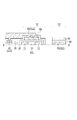
【選択図】図1
Description
GL1、GL2、GL3:ゲート金属配線
T1、T2、T3:静電気防止トランジスタ
C1、C2、C3:キャパシタ
10:真性半導体層領域
11、12:p型不純物ドーピング領域
20:ゲート絶縁層
30:層間絶縁層
40:クロック信号配線
50:ゲート電極層
60:ゲート金属配線
70:キャパシタの一電極
80:絶縁層
90:キャパシタの他電極
Claims (12)
- 映像を表示する表示部を駆動させる駆動回路と、前記駆動回路にクロック信号を伝達する少なくとも1つのクロック信号配線とを含む表示装置の静電気防止回路において、
前記静電気防止回路は、前記少なくとも1つのクロック信号配線それぞれと電気的に連結される少なくとも1つのトランジスタと、前記トランジスタのソース電極およびドレイン電極に共通に連結された一電極、および所定の固定電圧が印加される他電極を含む少なくとも1つのキャパシタとを含むことを特徴とする静電気防止回路。 - 前記少なくとも1つのクロック信号配線それぞれは、ゲート金属配線を介して前記少なくとも1つのトランジスタそれぞれのゲート電極に連結されることを特徴とする請求項1記載の静電気防止回路。
- 前記トランジスタは、半導体不純物でドーピングされた所定の不純物ドーピング領域、および前記半導体不純物でドーピングされない真性半導体領域を含む半導体層と、ゲート絶縁層を挟んで前記半導体層の上部に形成されたゲート電極層とを含み、
前記少なくとも1つのクロック信号配線を介して流入する静電気電流は、前記トランジスタのゲート絶縁層をオープンさせたりショートさせることを特徴とする請求項1記載の静電気防止回路。 - 前記半導体層の不純物ドーピング領域は、
第1不純物ドーピング領域と、前記第1不純物ドーピング領域に対向して形成され、前記ゲート電極層と重ならない領域で前記第1不純物ドーピング領域と電気的に連結される第2不純物ドーピング領域とを含むことを特徴とする請求項3記載の静電気防止回路。 - 前記ゲート絶縁層がショートする場合に、前記半導体層の不純物ドーピング領域と電気的に連結された一電極を含むキャパシタに前記流入した静電気電流が蓄積されることを特徴とする請求項3記載の静電気防止回路。
- 複数の画素を含み、前記複数の画素それぞれが映像データ信号によるデータ電圧に応じて発光して映像を表示する表示部と、
前記表示部を駆動させる駆動回路部と、
前記駆動回路部にクロック信号を伝達する少なくとも1つのクロック信号配線と、
前記少なくとも1つのクロック信号配線それぞれと電気的に連結される少なくとも1つのトランジスタと、前記トランジスタのソース電極およびドレイン電極に共通に連結された一電極、および所定の固定電圧が印加される他電極を含む少なくとも1つのキャパシタとを含む静電気防止回路とを含むことを特徴とする表示装置。 - 前記静電気防止回路は、前記少なくとも1つのクロック信号配線と前記駆動回路部との間に備えられることを特徴とする請求項6記載の表示装置。
- 前記少なくとも1つのクロック信号配線それぞれは、ゲート金属配線を介して前記静電気防止回路のトランジスタそれぞれのゲート電極に連結されることを特徴とする請求項6記載の表示装置。
- 前記トランジスタは、半導体不純物でドーピングされた所定の不純物ドーピング領域、および前記半導体不純物でドーピングされない真性半導体領域を含む半導体層と、ゲート絶縁層を挟んで前記半導体層の上部に形成されたゲート電極層とを含み、
前記キャパシタの一電極は、前記不純物ドーピング領域と電気的に連結されることを特徴とする請求項6記載の表示装置。 - 前記半導体層の不純物ドーピング領域は、
第1不純物ドーピング領域と、前記第1不純物ドーピング領域に対向して形成され、前記ゲート電極層と重ならない領域で前記第1不純物ドーピング領域と電気的に連結される第2不純物ドーピング領域とを含むことを特徴とする請求項9記載の表示装置。 - 前記トランジスタのゲート絶縁層は、少なくとも1つのクロック信号配線を介して流入する静電気電流によってオープンされたりショートすることを特徴とする請求項9記載の表示装置。
- 前記ゲート絶縁層がショートする場合に、前記半導体層の不純物ドーピング領域と電気的に連結された一電極を含むキャパシタに前記流入した静電気電流が蓄積されることを特徴とする請求項11記載の表示装置。
Applications Claiming Priority (2)
| Application Number | Priority Date | Filing Date | Title |
|---|---|---|---|
| KR1020130009434A KR102000738B1 (ko) | 2013-01-28 | 2013-01-28 | 정전기 방지 회로 및 이를 포함하는 표시 장치 |
| KR10-2013-0009434 | 2013-01-28 |
Publications (1)
| Publication Number | Publication Date |
|---|---|
| JP2014146777A true JP2014146777A (ja) | 2014-08-14 |
Family
ID=50023412
Family Applications (1)
| Application Number | Title | Priority Date | Filing Date |
|---|---|---|---|
| JP2013084890A Pending JP2014146777A (ja) | 2013-01-28 | 2013-04-15 | 静電気防止回路およびこれを含む表示装置 |
Country Status (6)
| Country | Link |
|---|---|
| US (5) | US9058770B2 (ja) |
| EP (1) | EP2759874B1 (ja) |
| JP (1) | JP2014146777A (ja) |
| KR (1) | KR102000738B1 (ja) |
| CN (1) | CN103972228B (ja) |
| TW (1) | TW201430807A (ja) |
Families Citing this family (18)
| Publication number | Priority date | Publication date | Assignee | Title |
|---|---|---|---|---|
| KR102000738B1 (ko) * | 2013-01-28 | 2019-07-23 | 삼성디스플레이 주식회사 | 정전기 방지 회로 및 이를 포함하는 표시 장치 |
| CN104749844A (zh) * | 2015-04-16 | 2015-07-01 | 上海中航光电子有限公司 | 静电防护电路、阵列基板、显示面板和显示装置 |
| KR102381283B1 (ko) * | 2015-07-24 | 2022-03-31 | 삼성디스플레이 주식회사 | 표시 장치 |
| KR102018440B1 (ko) | 2017-12-11 | 2019-09-04 | 한국식품연구원 | 지하저장고 및 그 운전방법 |
| KR101989703B1 (ko) | 2017-12-12 | 2019-06-14 | 한국식품연구원 | 지하저장고 유해기체 제거방법 |
| KR102508468B1 (ko) * | 2018-02-08 | 2023-03-10 | 삼성디스플레이 주식회사 | 표시 장치 |
| KR102505620B1 (ko) * | 2018-07-06 | 2023-03-02 | 엘지디스플레이 주식회사 | 디스플레이 패널, 디스플레이 장치 |
| KR102498797B1 (ko) * | 2018-09-28 | 2023-02-10 | 삼성디스플레이 주식회사 | 유기 발광 표시 장치 |
| CN208904019U (zh) * | 2018-11-22 | 2019-05-24 | 京东方科技集团股份有限公司 | 显示基板、静电放电保护电路和显示装置 |
| KR102595457B1 (ko) * | 2018-11-26 | 2023-10-27 | 엘지디스플레이 주식회사 | 정전기 방지회로를 포함한 유기발광 다이오드 표시장치용 어레이 기판 |
| KR102752455B1 (ko) * | 2019-09-09 | 2025-01-09 | 삼성디스플레이 주식회사 | 스캔 신호 구동부와 그를 포함한 표시 장치 |
| CN110767149B (zh) * | 2019-11-18 | 2021-10-22 | 合肥京东方卓印科技有限公司 | 栅极驱动电路、显示装置及修复方法 |
| CN111243473A (zh) | 2020-03-11 | 2020-06-05 | Tcl华星光电技术有限公司 | 源极驱动器静电起火防护方法及显示装置 |
| CN111240113B (zh) * | 2020-03-11 | 2021-07-06 | Tcl华星光电技术有限公司 | 阵列基板及显示面板 |
| KR102744149B1 (ko) * | 2020-05-04 | 2024-12-20 | 삼성디스플레이 주식회사 | 게이트 검사부 및 이를 포함하는 표시 장치 |
| KR102831083B1 (ko) * | 2021-02-09 | 2025-07-09 | 삼성디스플레이 주식회사 | 표시 장치 |
| KR20230139886A (ko) | 2022-03-24 | 2023-10-06 | 삼성디스플레이 주식회사 | 표시 장치 |
| TWI865105B (zh) * | 2023-10-17 | 2024-12-01 | 宏碁股份有限公司 | 可攜式電子裝置 |
Citations (4)
| Publication number | Priority date | Publication date | Assignee | Title |
|---|---|---|---|---|
| JP2001339051A (ja) * | 2000-05-30 | 2001-12-07 | Toshiba Corp | 回路素子の保護回路 |
| JP2006018165A (ja) * | 2004-07-05 | 2006-01-19 | Seiko Epson Corp | 半導体装置、表示装置及び電子機器 |
| JP2010097024A (ja) * | 2008-10-17 | 2010-04-30 | Epson Imaging Devices Corp | 液晶表示装置 |
| JP2011054936A (ja) * | 2009-09-03 | 2011-03-17 | Samsung Mobile Display Co Ltd | 有機発光表示装置及びその製造方法 |
Family Cites Families (38)
| Publication number | Priority date | Publication date | Assignee | Title |
|---|---|---|---|---|
| US4072976A (en) | 1976-12-28 | 1978-02-07 | Hughes Aircraft Company | Gate protection device for MOS circuits |
| DE3929161A1 (de) | 1989-09-02 | 1991-03-07 | Bosch Gmbh Robert | Halbleiterbauelement |
| US5345357A (en) * | 1992-06-05 | 1994-09-06 | At&T Bell Laboratories | ESD protection of output buffers |
| JPH06186590A (ja) | 1992-12-21 | 1994-07-08 | Sharp Corp | アクティブマトリクス型液晶表示パネル |
| JPH10198292A (ja) * | 1996-12-30 | 1998-07-31 | Semiconductor Energy Lab Co Ltd | 半導体装置およびその作製方法 |
| JP4516638B2 (ja) | 1997-10-14 | 2010-08-04 | 三星電子株式会社 | 液晶表示装置用基板、液晶表示装置及びその製造方法 |
| KR100299686B1 (ko) | 1997-10-14 | 2001-10-27 | 윤종용 | 정전기방전기능을가지는액정표시장치및그제조방법 |
| KR100598735B1 (ko) * | 1999-09-21 | 2006-07-10 | 엘지.필립스 엘시디 주식회사 | 액정표시소자의 정전기 방지회로 |
| US7256421B2 (en) * | 2002-05-17 | 2007-08-14 | Semiconductor Energy Laboratory, Co., Ltd. | Display device having a structure for preventing the deterioration of a light emitting device |
| JP3772889B2 (ja) * | 2003-05-19 | 2006-05-10 | セイコーエプソン株式会社 | 電気光学装置およびその駆動装置 |
| US7262753B2 (en) * | 2003-08-07 | 2007-08-28 | Barco N.V. | Method and system for measuring and controlling an OLED display element for improved lifetime and light output |
| US7405713B2 (en) * | 2003-12-25 | 2008-07-29 | Semiconductor Energy Laboratory Co., Ltd. | Light emitting device and electronic equipment using the same |
| KR100557730B1 (ko) * | 2003-12-26 | 2006-03-06 | 엘지.필립스 엘시디 주식회사 | 듀얼패널타입 유기전계발광 소자 및 그 제조방법 |
| KR100636483B1 (ko) | 2004-06-25 | 2006-10-18 | 삼성에스디아이 주식회사 | 트랜지스터와 그의 제조방법 및 발광 표시장치 |
| TWI281740B (en) | 2004-09-08 | 2007-05-21 | Winbond Electronics Corp | Electrostatic discharge protection circuit |
| KR100667075B1 (ko) * | 2005-07-22 | 2007-01-10 | 삼성에스디아이 주식회사 | 주사 구동부 및 이를 포함하는 유기 전계발광 표시장치 |
| TWI306358B (en) | 2006-02-17 | 2009-02-11 | Himax Tech Inc | Organic light emitting display and pixel circuit thereof |
| JP4203770B2 (ja) * | 2006-05-29 | 2009-01-07 | ソニー株式会社 | 画像表示装置 |
| TWI385621B (zh) * | 2006-08-01 | 2013-02-11 | Casio Computer Co Ltd | 顯示驅動裝置及其驅動方法、以及顯示裝置及其驅動方法 |
| JP2008058940A (ja) * | 2006-08-02 | 2008-03-13 | Sony Corp | 表示装置、表示装置の駆動方法および電子機器 |
| JP4211820B2 (ja) * | 2006-08-15 | 2009-01-21 | ソニー株式会社 | 画素回路と画像表示装置及びその駆動方法 |
| JP2008046377A (ja) * | 2006-08-17 | 2008-02-28 | Sony Corp | 表示装置 |
| KR100839750B1 (ko) | 2007-01-15 | 2008-06-19 | 삼성에스디아이 주식회사 | 유기 전계 발광 표시 장치 |
| KR101437868B1 (ko) * | 2007-11-14 | 2014-09-05 | 삼성디스플레이 주식회사 | 표시 장치 |
| JP4807365B2 (ja) | 2008-03-10 | 2011-11-02 | セイコーエプソン株式会社 | 半導体装置、表示装置および電子機器 |
| CN101359024B (zh) | 2008-09-23 | 2012-05-30 | 友达光电(苏州)有限公司 | 电子装置显示面板的测试电路和显示面板 |
| KR20100073009A (ko) * | 2008-12-22 | 2010-07-01 | 한국전자통신연구원 | 다단 듀얼 연속 근사 레지스터 아날로그 디지털 변환기 및 이를 이용한 아날로그 디지털 변환 방법 |
| TWI596741B (zh) * | 2009-08-07 | 2017-08-21 | 半導體能源研究所股份有限公司 | 半導體裝置和其製造方法 |
| JP5663231B2 (ja) * | 2009-08-07 | 2015-02-04 | 株式会社半導体エネルギー研究所 | 発光装置 |
| WO2011027701A1 (en) * | 2009-09-04 | 2011-03-10 | Semiconductor Energy Laboratory Co., Ltd. | Light-emitting device and method for manufacturing the same |
| KR101330421B1 (ko) * | 2009-12-08 | 2013-11-15 | 엘지디스플레이 주식회사 | 게이트 인 패널 구조의 액정표시장치 |
| KR101113354B1 (ko) * | 2010-04-16 | 2012-02-29 | 삼성모바일디스플레이주식회사 | 표시 장치 및 그 제조방법 |
| JP5489844B2 (ja) * | 2010-04-27 | 2014-05-14 | 富士フイルム株式会社 | 電子装置 |
| CN101859764B (zh) * | 2010-06-03 | 2012-02-08 | 友达光电股份有限公司 | 静电防护电路及采用此种静电防护电路的显示装置 |
| KR101815255B1 (ko) | 2010-12-16 | 2018-01-08 | 삼성디스플레이 주식회사 | 유기전계발광표시장치 및 이에 적용되는 입력패드 |
| TWI405325B (zh) | 2011-01-19 | 2013-08-11 | Global Unichip Corp | 靜電放電保護電路 |
| JP5724623B2 (ja) * | 2011-05-23 | 2015-05-27 | ソニー株式会社 | 信号伝達装置および撮像表示システム |
| KR102000738B1 (ko) * | 2013-01-28 | 2019-07-23 | 삼성디스플레이 주식회사 | 정전기 방지 회로 및 이를 포함하는 표시 장치 |
-
2013
- 2013-01-28 KR KR1020130009434A patent/KR102000738B1/ko active Active
- 2013-04-15 JP JP2013084890A patent/JP2014146777A/ja active Pending
- 2013-08-01 US US13/957,371 patent/US9058770B2/en active Active
- 2013-10-17 TW TW102137579A patent/TW201430807A/zh unknown
- 2013-12-05 CN CN201310653295.8A patent/CN103972228B/zh active Active
-
2014
- 2014-01-08 EP EP14150424.1A patent/EP2759874B1/en active Active
-
2015
- 2015-05-08 US US14/708,116 patent/US10026798B2/en active Active
-
2018
- 2018-07-16 US US16/036,847 patent/US10199450B2/en active Active
- 2018-12-26 US US16/233,065 patent/US10461144B2/en active Active
-
2019
- 2019-10-28 US US16/665,958 patent/US10886357B2/en active Active
Patent Citations (4)
| Publication number | Priority date | Publication date | Assignee | Title |
|---|---|---|---|---|
| JP2001339051A (ja) * | 2000-05-30 | 2001-12-07 | Toshiba Corp | 回路素子の保護回路 |
| JP2006018165A (ja) * | 2004-07-05 | 2006-01-19 | Seiko Epson Corp | 半導体装置、表示装置及び電子機器 |
| JP2010097024A (ja) * | 2008-10-17 | 2010-04-30 | Epson Imaging Devices Corp | 液晶表示装置 |
| JP2011054936A (ja) * | 2009-09-03 | 2011-03-17 | Samsung Mobile Display Co Ltd | 有機発光表示装置及びその製造方法 |
Also Published As
| Publication number | Publication date |
|---|---|
| EP2759874B1 (en) | 2017-04-05 |
| US10461144B2 (en) | 2019-10-29 |
| CN103972228B (zh) | 2018-03-27 |
| US20180342573A1 (en) | 2018-11-29 |
| US20150243726A1 (en) | 2015-08-27 |
| US10886357B2 (en) | 2021-01-05 |
| CN103972228A (zh) | 2014-08-06 |
| US9058770B2 (en) | 2015-06-16 |
| US20200066823A1 (en) | 2020-02-27 |
| KR102000738B1 (ko) | 2019-07-23 |
| US10199450B2 (en) | 2019-02-05 |
| US10026798B2 (en) | 2018-07-17 |
| US20190131380A1 (en) | 2019-05-02 |
| TW201430807A (zh) | 2014-08-01 |
| US20140210807A1 (en) | 2014-07-31 |
| KR20140096634A (ko) | 2014-08-06 |
| EP2759874A1 (en) | 2014-07-30 |
Similar Documents
| Publication | Publication Date | Title |
|---|---|---|
| JP2014146777A (ja) | 静電気防止回路およびこれを含む表示装置 | |
| US11876099B2 (en) | Displays with silicon and semiconducting oxide thin-film transistors | |
| KR101739526B1 (ko) | 유기 발광 표시 장치 | |
| US9761578B2 (en) | Display device including electrostatic discharge circuit | |
| JP7510350B2 (ja) | アレイ基板及び表示装置 | |
| US9301377B2 (en) | Circuit for preventing static electricity of a display panel and display device including the same | |
| KR102181003B1 (ko) | 정전기 방지 회로 및 이를 포함하는 표시 장치 | |
| KR102077327B1 (ko) | 정전기 방지 회로 및 이를 포함하는 표시 장치 | |
| KR20240126501A (ko) | 표시 장치 |
Legal Events
| Date | Code | Title | Description |
|---|---|---|---|
| A621 | Written request for application examination |
Free format text: JAPANESE INTERMEDIATE CODE: A621 Effective date: 20160411 |
|
| A977 | Report on retrieval |
Free format text: JAPANESE INTERMEDIATE CODE: A971007 Effective date: 20170206 |
|
| A131 | Notification of reasons for refusal |
Free format text: JAPANESE INTERMEDIATE CODE: A131 Effective date: 20170328 |
|
| RD02 | Notification of acceptance of power of attorney |
Free format text: JAPANESE INTERMEDIATE CODE: A7422 Effective date: 20170421 |
|
| A02 | Decision of refusal |
Free format text: JAPANESE INTERMEDIATE CODE: A02 Effective date: 20171114 |