JP2014162012A - Microstructure molding method and microstructure molding die - Google Patents
Microstructure molding method and microstructure molding die Download PDFInfo
- Publication number
- JP2014162012A JP2014162012A JP2013031942A JP2013031942A JP2014162012A JP 2014162012 A JP2014162012 A JP 2014162012A JP 2013031942 A JP2013031942 A JP 2013031942A JP 2013031942 A JP2013031942 A JP 2013031942A JP 2014162012 A JP2014162012 A JP 2014162012A
- Authority
- JP
- Japan
- Prior art keywords
- mold
- microstructure
- coating film
- flat
- fine structure
- Prior art date
- Legal status (The legal status is an assumption and is not a legal conclusion. Google has not performed a legal analysis and makes no representation as to the accuracy of the status listed.)
- Pending
Links
Images

Landscapes
- Moulds For Moulding Plastics Or The Like (AREA)
- Casting Or Compression Moulding Of Plastics Or The Like (AREA)
Abstract
【課題】縁端部にバリがないばかりでなく微細構造が平面部及び一の縁端部に転写成形された平板状の微細構造体を成形することができる方法及び金型を提供する。
【解決手段】本発明に係る微細構造体成形方法は、下金型に溶融樹脂を塗布して形成した塗膜を、上金型により押圧し、前記塗膜の平面部と一の縁端部に微細構造を転写成形してこれを冷却固化し、前記平面部と一の縁端部に前記微細構造を有するとともに、前記一の縁端部にバリのない平板状の微細構造体を成形する方法であって、前記下金型に、平板状の塗膜を形成する段階と、前記上金型を水平面から傾斜させた状態でその下端の先端部を前記下金型に当接させた後、その当接部を中心に前記上金型が水平になるまで回転させるとともに押圧し、前記塗膜の平面部及び一の縁端部に前記微細構造の転写成形を行うことにより実施される。
【選択図】図1The present invention provides a method and a mold capable of molding a flat microstructure having not only burrs at the edge but also having a microstructure transferred and formed on a flat surface and one edge.
A method for forming a microstructure according to the present invention comprises pressing a coating film formed by applying a molten resin to a lower mold with an upper mold, and a flat portion and one edge portion of the coating film. The fine structure is transferred and molded, and this is cooled and solidified, and the flat structure having the fine structure at one edge and the flat edge and having no burr at the one edge is formed. A method of forming a flat coating film on the lower mold, and after contacting the tip of the lower end with the lower mold in a state where the upper mold is inclined from a horizontal plane Then, the upper mold is rotated and pressed around the contact portion until it becomes horizontal, and the fine structure is transferred and formed on the flat portion and one edge portion of the coating film.
[Selection] Figure 1
Description
本発明は、微細構造を有する金型に熱可塑性の溶融樹脂を押圧し、その微細構造が平面部及び一の縁端部に転写成形された平板状の微細構造体を成形する方法及び金型に関する。 The present invention relates to a method and a mold for pressing a molten thermoplastic resin onto a mold having a fine structure, and forming a flat fine structure having the fine structure transferred and formed on a flat portion and one edge portion. About.
微細構造を有する薄い板状体のマイクロレンズアレイや導光板などが、プレス成形法、射出成形法あるいは押出成形法により微細構造を有する金型あるいはロールに熱可塑性樹脂の溶融体を押圧し、これを冷却・固化することによって成形されている。これらの方法は、各種の熱可塑性樹脂を成形することができる利点を有し、その応用・利用範囲が拡大している。 A micro-lens array or light guide plate with a thin plate having a fine structure presses a thermoplastic resin melt onto a mold or roll having a fine structure by a press molding method, an injection molding method or an extrusion molding method. Is formed by cooling and solidifying. These methods have an advantage that various thermoplastic resins can be molded, and their application and use range is expanded.
例えば、特許文献1に、熱可塑性樹脂が供給された塗布装置を微細な凹凸部を有する成形型上に移動させながらその微細な凹凸部に前記熱可塑性樹脂を充填し、その塗布した熱可塑性樹脂を金型によりプレスした後、冷却し固化させる成形体の製造方法が開示されている。この成形体の製造方法によると、10nm〜1mmの凹凸をなす微細構造を有する厚さ50μm〜5mmの平板状の微細構造体を成形することができるとされる。 For example, in Patent Document 1, while moving a coating apparatus supplied with a thermoplastic resin onto a mold having fine uneven portions, the thermoplastic resin is filled in the fine uneven portions, and the applied thermoplastic resin A method for producing a molded body is disclosed in which the material is pressed by a mold and then cooled and solidified. According to this method of manufacturing a molded body, it is said that a flat microstructure having a thickness of 50 μm to 5 mm and having a microstructure having irregularities of 10 nm to 1 mm can be molded.
特許文献2には、環状オレフィン系樹脂組成物を射出成形してなる導光板であって、前記導光板は厚み(T)が0.1mm以上1mm以下であり、導光板に対して光が入射する方向の幅(L)と厚み(T)との比(L/T)が70以上の平板状をなしており、光射出面内の最大輝度と最小輝度との比(最大輝度/最小輝度)が1.05以下である導光板が開示されている。この導光板は、射出速度の最大値である最大射出速度を制御する射出速度制御部と、射出開始から最大射出速度に到達するまでの間の射出加速度を制御する射出加速度制御部とを備える射出成形機を用いて製造することができるとされる。 Patent Document 2 discloses a light guide plate formed by injection-molding a cyclic olefin-based resin composition, and the light guide plate has a thickness (T) of 0.1 mm to 1 mm, and light enters the light guide plate. The ratio (L / T) of the width (L) to the thickness (T) in the direction is 70 or more, and the ratio between the maximum brightness and the minimum brightness in the light exit plane (maximum brightness / minimum brightness) A light guide plate having a thickness of 1.05 or less is disclosed. The light guide plate includes an injection speed control unit that controls a maximum injection speed that is a maximum value of the injection speed, and an injection acceleration control unit that controls an injection acceleration from the start of injection until the maximum injection speed is reached. It can be manufactured using a molding machine.
このようなプレス成形法や射出成形法など金型を使用する成形法は、上金型と下金型又は可動金型と固定金型により溶融樹脂を充填するキャビティが形成されるようになっており、金型の合わせ面(パーティングライン)にバリが生じやすいという問題がある。このバリの発生を防止する方法として、例えば、特許文献3に示す方法が提案されている。すなわち、射出成形金型の固定側スタンパ、可動側スタンパ及び可動側スタンパの外周部を進退する外周リングにより溶融樹脂を充填するキャビティが形成される金型において、可動側スタンパの外周面と外周リングの内周面との隙間をベアリングにより1μm〜30μmに確保する情報記録ディスク基板成形金型が開示されている。 Molding methods using a mold such as the press molding method and the injection molding method are such that a cavity for filling a molten resin is formed by an upper die and a lower die or a movable die and a fixed die. In addition, there is a problem that burrs are likely to occur on the mating surface (parting line) of the mold. As a method for preventing the occurrence of this burr, for example, a method disclosed in Patent Document 3 has been proposed. That is, in a mold in which a cavity filled with a molten resin is formed by a fixed stamper of an injection mold, a movable stamper, and an outer ring that advances and retreats the outer periphery of the movable stamper, the outer peripheral surface and the outer ring of the movable stamper An information recording disk substrate molding die is disclosed in which a clearance from the inner peripheral surface of the substrate is secured to 1 μm to 30 μm by a bearing.
一方、金型を使用しない成形法も提案されており、特許文献4には、回転駆動ロールと成形ロールとの挟部に供給された溶融樹脂を加圧して微細構造を賦形する押出成形法により光学シートを成形する方法が開示されている。すなわち、押出成形法により成形することができる、エッジライト方式の面光源装置に用いられ、少なくとも一方の面に複数の単位光学形状が配列された光学シートであって、シート面に直交する1つの方向において、その厚さが連続的に変化しており、前記1つの方向における該光学シートの少なくとも一方の端部から他方の端部側に向かってしだいに厚みが薄くなっている部分を有する光学シートが開示されている。 On the other hand, a molding method that does not use a mold has also been proposed, and Patent Document 4 discloses an extrusion molding method in which a molten resin supplied to a sandwiched portion between a rotary drive roll and a molding roll is pressurized to form a fine structure. Discloses a method of forming an optical sheet. That is, an optical sheet that is used in an edge light type surface light source device that can be molded by an extrusion molding method, and in which a plurality of unit optical shapes are arranged on at least one surface, An optical element having a thickness that continuously changes in the direction, and a portion in which the thickness gradually decreases from at least one end of the optical sheet toward the other end in the one direction. A sheet is disclosed.
また、特許文献5には、シリカ等の微細粒子又は気泡が分散した層を挟んで3層からなる導光板が共押出し成形法により成形されることが開示されている。すなわち、エッジライト型光源を有する表示装置に用いられる導光板であり、かつ、画像表示パネル側に光を照射する光射出面と、前記光射出面に対向する面である反光射出面と、前記二面に略垂直な少なくとも一面である光入射面とを有する熱可塑性樹脂からなる厚さが0.5〜4mmの導光板が提案されている。この導光板は、高い正面輝度と均一な輝度分布を有し、大量生産が可能であるとされる。 Patent Document 5 discloses that a three-layer light guide plate is formed by a coextrusion molding method with a layer in which fine particles such as silica or bubbles are dispersed. That is, a light guide plate used in a display device having an edge light type light source, and a light emission surface that irradiates light to the image display panel side, a counter light emission surface that is a surface facing the light emission surface, and A light guide plate having a thickness of 0.5 to 4 mm made of a thermoplastic resin having at least one light incident surface substantially perpendicular to the two surfaces has been proposed. This light guide plate has high front luminance and uniform luminance distribution, and can be mass-produced.
微細構造を有する微細構造体は、ますます薄いものが求められており、微細構造が平板状の微細構造体の表面又は/及び裏面に設けられたものが求められている。また、導光板は、微細構造体の縁端部が鏡面になってことが必要であるが、この縁端部にまで微細構造を有するものが求められている。このような、微細構造が薄い平板状の微細構造体の所望の面に設けられた微細構造体を成形するには、特許文献4又は5に記載さているような押出法は押出方向と直角な方向(薄い平板状の微細構造体の側面へ)の転写成形が難しく好ましくない。これに対し、金型によりキャビティを形成する特許文献1又は2に記載されているようなプレス成形法や射出成形法が好ましい。 The fine structure having a fine structure is required to be thinner and thinner, and the fine structure is required to be provided on the front surface and / or the back surface of the flat fine structure. Further, the light guide plate needs to have a mirror surface at the edge of the fine structure, but a light guide plate having a fine structure up to the edge is required. In order to form such a fine structure provided on a desired surface of a flat plate-like fine structure, the extrusion method described in Patent Document 4 or 5 is perpendicular to the extrusion direction. Transfer molding in the direction (to the side of the thin flat microstructure) is difficult and undesirable. On the other hand, a press molding method or an injection molding method as described in Patent Document 1 or 2 in which a cavity is formed by a mold is preferable.
しかしながら、金型を使用する場合は、上述のようにバリ発生の問題がある。特許文献2に記載するような射出成形法の場合は、特許文献3に記載するように金型の合わせ面における隙間をゼロにするのは難しくバリの発生のおそれがある。また、射出成形法は、金型のキャビティ内に溶融樹脂を充填するゲートから薄い平板状のキャビティの隅々に溶融樹脂が流動する過程で樹脂の温度が低下して粘度が増大または固化するため、キャビティの隅々まで充填するのが難しく、キャビティ縁端部に加工された微細構造を溶融樹脂に転写することはさらに困難であるため、縁端部に微細構造を有する平板状の微細構造体を成形するのが容易でないという問題がある。 However, when a mold is used, there is a problem of burrs as described above. In the case of the injection molding method described in Patent Document 2, it is difficult to make the gap on the mating surface of the molds zero as described in Patent Document 3, and there is a risk of burrs. In the injection molding method, the temperature of the resin decreases and the viscosity increases or solidifies during the process of flowing the molten resin from the gate filling the molten resin into the mold cavity to every corner of the thin flat cavity. Since it is difficult to fill every corner of the cavity and it is further difficult to transfer the microstructure processed at the edge of the cavity to the molten resin, a flat microstructure having a microstructure at the edge There is a problem that it is not easy to mold.
一方、特許文献1に記載するプレス成形法は、非常に薄い平板状の微細構造体を成形することができるという利点があるが、微細構造を溶融樹脂に転写成形する金型の温度が高いので、1μm以下の隙間でも溶融樹脂が進入するためバリが発生しやすく、バリのない縁端部の成形が容易でないという問題がある。 On the other hand, the press molding method described in Patent Document 1 has an advantage that a very thin plate-like microstructure can be molded, but the temperature of the mold for transferring the microstructure to the molten resin is high. Further, since the molten resin enters even in a gap of 1 μm or less, there is a problem that burrs are easily generated, and it is not easy to form an edge portion without burrs.
本発明は、このような従来の問題点及び技術的な要請に鑑み、より薄い平板状の微細構造体の成形法に好適なプレス成形法を使用し、縁端部にバリがないばかりでなく微細構造が平面部及び一の縁端部に転写成形された平板状の微細構造体を成形することができる微細構造体成形方法及び微細構造体成形金型を提供することを目的とする。 In view of such conventional problems and technical demands, the present invention uses a press molding method suitable for the molding method of a thinner flat plate-like microstructure, and not only has no burrs at the edges. It is an object of the present invention to provide a fine structure forming method and a fine structure forming mold capable of forming a flat fine structure having a fine structure transferred to a flat portion and one edge portion.
本発明に係る微細構造体成形方法は、下金型に溶融樹脂を塗布して形成した塗膜を、上金型により押圧し、前記塗膜の平面部と一の縁端部に微細構造を転写成形してこれを冷却固化し、前記平面部と一の縁端部に前記微細構造を有するとともに、前記一の縁端部にバリのない平板状の微細構造体を成形する方法であって、前記下金型に、平板状の塗膜を形成する段階と、前記上金型を水平から傾斜させた状態でその下端の先端部を前記下金型に当接させた後、その当接部を中心に前記上金型が水平になるまで回転させるとともに押圧し、前記塗膜の平面部及び一の縁端部に前記微細構造の転写成形を行うことにより実施される。なお、水平とは、プレス成形法において上金型及び下金型が水平(金型設置平面又はプレス成形面が水平)に設置された通常の形態を前提にしており、下金型の設置平面が傾斜していれば、その傾斜した設置平面が基準になる。 In the microstructure forming method according to the present invention, a coating film formed by applying a molten resin to a lower mold is pressed by an upper mold, and a microstructure is formed on a flat portion and one edge of the coating film. This is a method of forming a flat microstructure having a fine structure at the edge portion of the flat portion and having no burrs at the edge portion of the one side, which is formed by transfer molding and cooled and solidified. A step of forming a flat coating film on the lower mold, and abutting the tip of the lower end with the lower mold in a state where the upper mold is inclined from the horizontal, and then contacting the lower mold This is carried out by rotating and pressing the upper mold until the upper mold becomes horizontal, centering on the portion, and performing transfer molding of the fine structure on the flat portion and one edge portion of the coating film. The term “horizontal” is based on the normal form in which the upper mold and the lower mold are installed horizontally (the mold installation plane or the press molding surface is horizontal) in the press molding method. Is inclined, the inclined installation plane is the reference.
上記発明において、上金型の下端の先端部と下金型との接触面圧は、塗膜の押圧中に溶融樹脂が前記上金型と前記下金型との金型合わせ面に侵入するのを防止できる以上の大きさであるのがよい。 In the above invention, the contact surface pressure between the lower end of the upper mold and the lower mold is such that the molten resin enters the mold mating surface of the upper mold and the lower mold during the pressing of the coating film. It is preferable that the size is larger than that which can be prevented.
また、塗膜は、その一の縁端部がこれに微細構造の転写成形を行う上金型の前面から0mmを越え5mm以下離れた位置から形成されるようにするのがよい。そして、塗膜は、一の縁端部側が厚くなって凸条が形成された平板状のものにすることができ、塗膜の凸条部の厚さteは0.05〜5mm、平面部の厚さtは0.05〜5mm、te−tは0〜1mmにすることができる。 Further, the coating film is preferably formed so that one edge portion thereof is located at a position exceeding 0 mm and not more than 5 mm from the front surface of the upper mold on which the fine structure is transferred. The coating may be of one edge side is thicker shaped plates projecting strip is formed, the thickness t e of the convex portion of the coating 0.05 to 5 mm, the flat portion the thickness t is 0.05 to 5 mm, t e -t can be 0 to 1 mm.
また、上金型は、塗膜の平面部の天面の転写成形を行う上面型部と一の縁端部の転写成形を行う端面型部とを有するものとすることができ、下金型は、塗膜の平面部の地面の転写成形を行う下面型部を有するものとすることができる。 The upper mold may have an upper surface mold part that performs transfer molding of the top surface of the flat part of the coating film and an end surface mold part that performs transfer molding of one edge part. May have a lower surface mold part for performing transfer molding of the ground surface of the flat part of the coating film.
微細構造の転写成形が行われる塗膜の平面部は、天面又は/及び底面とすることができる。 The flat surface portion of the coating film on which the fine structure transfer molding is performed can be the top surface and / or the bottom surface.
本発明に係る微細構造体成形金型は、下金型に溶融樹脂を塗布して形成した塗膜を、微細構造を有する上金型により押圧し、前記塗膜の平面部と一の縁端部に前記微細構造を転写成形してこれを冷却固化し、前記平面部と一の縁端部に前記微細構造を有する平板状の微細構造体を成形する微細構造体成形金型であって、上母型に弾性部材を介して保持される上型部が前記平面部の転写成形を行う上面型部と、前記一の縁端部の転写成形を行う端面型部とを有する上金型と、前記上金型に対向する下金型を有し、前記上金型は、前記弾性部材により水平から傾斜させた状態になるようになっている。 The fine structure molding die according to the present invention is such that a coating film formed by applying a molten resin to a lower mold is pressed by an upper mold having a fine structure, and a flat portion of the coating film and one edge. A microstructure forming mold for forming a flat microstructure having the microstructure on one edge of the flat portion by transferring and molding the microstructure to a part and cooling and solidifying the planar structure; An upper mold having an upper mold part that performs transfer molding of the flat surface part, and an end mold part that performs transfer molding of the one edge part, and an upper mold part held by an elastic member via an elastic member; The lower mold is opposed to the upper mold, and the upper mold is inclined from the horizontal by the elastic member.
上記、微細構造体成形金型において、弾性部材は、一の端面型部側の方がその他方の側よりも厚くなっているものとすることができる。 In the above microstructured mold, the elastic member may be thicker on one end face mold part side than on the other side.
また、上金型の上型部の傾斜角度θは、θ=0.001〜1°であるのがよく、上型部の端面型部が下金型と接触する部分に干渉部材が設けられているのがよい。 In addition, the inclination angle θ of the upper mold part of the upper mold is preferably θ = 0.001 to 1 °, and an interference member is provided at a part where the end face mold part of the upper mold part contacts the lower mold. It is good.
本発明によれば、平板状の薄くて表面又は/及び裏面、または、一の縁端部等の所望の部位に微細構造を有する微細構造体を成形することができる。そして、本発明によれば、成形された微細構造体の一の縁端部にバリがなく、その縁端部の切断除去あるいはバリ取り等の作業を要しない。また、本発明に係る微細構造体成形金型は、特別の構造を要せず、また、特別の操作も要しない。 ADVANTAGE OF THE INVENTION According to this invention, the fine structure which has a fine structure in desired site | parts, such as the flat thin surface and / or back surface, or one edge part, can be shape | molded. And according to this invention, there is no burr | flash in one edge part of the shape | molded microstructure, and work, such as cutting removal of the edge part, or a deburring, is not required. Moreover, the fine structure molding die according to the present invention does not require a special structure and does not require any special operation.
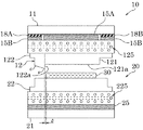
以下、本発明を実施するための形態について説明する。本発明に係る微細構造体成形方法は、図1に示す微細構造体成形金型により好適に実施することができる。図1において、上金型10は、弾性部材18(18A、18B)を介して上母型11に保持された上型部12を有している。上型部12は、温度制御手段125を有し、また、上母型11と断熱部材15(15A、15B)を介して保持されるようになっている。そして、上型部12は、121aの面に微細構造が設けられた上面型部121と、122aの面に微細構造が設けられた端面型部122を有し、端面型部122の先端部に逃げ部dが設けられている。
Hereinafter, modes for carrying out the present invention will be described. The microstructure forming method according to the present invention can be preferably carried out by the microstructure forming mold shown in FIG. In FIG. 1, an
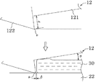
下金型20は、下母型21に保持された下型部22を有している。下型部22は、温度制御手段225を有し、断熱部材25を介して下母型21に保持されている。下型部22の上面には、溶融した熱可塑性樹脂を塗布して塗膜30を形成することができるようになっている。この微細構造体成形金型において、弾性部材18は、弾性部材18Aと弾性部材18Bとの厚さが異なり、上型部12は、図2に示すように水平から傾斜した状態になっている。
The
本微細構造体成形方法は、このような微細構造体成形金型を使用して好適に実施される方法であり、下金型20に溶融樹脂を塗布して形成した塗膜30を、上金型10により押圧し、塗膜30の平面部と一の縁端部に微細構造を転写成形してこれを冷却固化し、前記平面部と一の縁端部に前記微細構造を有するとともに、前記一の縁端部にバリのない平板状の微細構造体を成形する方法である。
This microstructure forming method is a method that is preferably performed using such a microstructure forming mold, and a
すなわち、本微細構造体成形方法は、先ず、下金型20の下型部22に、平板状の塗膜30を形成する。塗膜30は、熱可塑性の溶融樹脂をその上面にゲージ圧で動圧0.1〜5MPaを与えるようにTダイにより塗布するのがよい。これにより、高精度に塗膜30の厚さを制御することができ、最終製品としての微細構造体の厚さを高精度に制御することができる。また、このTダイによる塗布においては、面内の厚み分布(最も厚い部分と最も薄い部分との差)を10μm前後に抑えることができる。すなわち、Tダイからの樹脂吐出部を塗膜の厚みとほぼ同じ距離まで下型部22の被塗布面に近接させてTダイを移動させ、Tダイからの樹脂の吐出幅とTダイの移動速度およびTダイの樹脂吐出部と下型部水平面との距離の乗算で算出される体積流量にほぼ等しい流量の溶融樹脂を吐出部から吐出しながら塗布する。これにより、塗膜の幅はTダイからの樹脂吐出部の幅、塗膜の長さはTダイの移動距離とほぼ等しくすることができる。そして、これらにより、塗膜の幅、長さおよび厚みは、押圧後に得られる最終的な微細構造体とほぼ等しい形状および厚みに精度良く塗布することができる。
That is, in this microstructure forming method, first, the
本発明において塗膜30は、図1又は図2に示すように、上型部12の端面型部122の前面から隙間δを有するように下型部22に塗布されて形成される。隙間δは、先端部pが下型部22に当接するよりも前に先端部pと下型部22との隙間に溶融樹脂が入り込まないように適切な値が選択される。例えば、端面型部のh寸法に対して塗膜の凸条部の厚さteが相対的に厚いと隙間δは大きくする必要があり、逆にh寸法に対して凸条部の厚さteがわずかに厚い程度ならば隙間δは小さくする必要があるが、概ね隙間δは0mmを越え5mm以下とされる。
In the present invention, as shown in FIG. 1 or 2, the
また、塗膜30は、一般的には下型部22に平板状に塗布することにより形成されるが、図3に示すように一の縁端部30cが凸条に厚くなった板状体に形成することができる。このような塗膜30は、例えば、凸条部の厚さte=0.05〜5mm、平面部の厚さt=0.05〜5mm、(te−t)=0〜1mmとすることができる。このような一の縁端部30cが厚くなった形状の塗膜30は、上記隙間δの大きさにも依るが、微細構造を一の縁端部30cに高精度で転写成形する場合に好都合である。
The
上記のように塗膜30が形成されると、次に、上金型10を下降させる。上金型10は、図2に示すように、上型部12が水平から傾斜した状態になっているので、先ずその下端の先端部pが下金型20の下型部22に当接する。そして、先端部pからの反力により上金型10に設けた弾性部材18Aと弾性部材18Bが圧縮され、塗膜30が上面型部121により圧縮されるようになる。この、上面型部121による塗膜30の押圧により塗膜内に微小な流動を生じ、上面型部121、端面型部122及び下型部22により形成されるキャビティ内で塗膜30の天面30a及び一の縁端部30cに微細構造の転写成形が行われる。押圧力は、1〜10MPaとされる。なお、下型部22が微細構造を有する場合は、塗膜30bの底面にもその微細構造の転写成形を行うことができる。
When the
塗膜30の転写成形において、先端部pに負荷される面圧は、塗膜30の押圧中に溶融樹脂が先端部pに入り込まない程度にされる。これにより、塗膜30の一の縁端部30cにバリのない微細構造体を成形することができる。
In the transfer molding of the
上記塗膜30の転写成形において、上型部12は先端部pを回転中心として回転(図2において右回り)した挙動をする。すなわち、本発明においては、上金型を水平から傾斜させた状態でその下端の先端部を下金型に当接させた後、その当接部を中心に前記上金型が水平になるまで回転させるとともに押圧することができるような方法であればよい。
In the transfer molding of the
本微細構造体成形方法は、平面部(天面又は/及び底面)と一の縁端部に微細構造を有する平板状の微細構造体を成形することができ、転写成形において一の縁端部にバリを生じないことが特徴である。このため、上述のように、上型部12には微細構造を有する上面型部121と端面型部122が設けられている。この上面型部121と端面型部122は一体で、金型合わせ面がないものが好ましい。金型合わせ面があると、この部分にバリを生じる恐れがあり、この部分に上述の上型部12の先端部pのような構造を設ける必要を生じるからである。しかしながら、上面型部121と端面型部122は分解可能に構成されているのがよい。微細構造体の平面部と縁端部の微細構造は、その形態が全く異なることが多く、特に縁端部の微細構造は種々の形態のものができるようになっているのが好ましいからである。
This fine structure forming method can form a flat fine structure having a fine structure on a flat portion (top surface or / and bottom surface) and one edge, and one edge in transfer molding. It is characterized by no burrs. Therefore, as described above, the
本微細構造体成形方法に使用される熱可塑性樹脂は、種々の熱可塑性樹脂を使用することができる。例えば、ポリカーボネート(PC)、ポリメタクリル酸メチル(PMMA)、シクロオレフィンポリマー(COP)、環状オレフィンコポリマー(COC)、ポリエチレンテレフタレート(PET)、ポリエチレンナフタレート(PEN)、ポリスチレン(PS)、メチルメタクリレートブタジエンスチレン(MBS)などの樹脂材料を好適に使用することができる。 Various thermoplastic resins can be used as the thermoplastic resin used in the present microstructure forming method. For example, polycarbonate (PC), polymethyl methacrylate (PMMA), cycloolefin polymer (COP), cyclic olefin copolymer (COC), polyethylene terephthalate (PET), polyethylene naphthalate (PEN), polystyrene (PS), methyl methacrylate butadiene Resin materials such as styrene (MBS) can be suitably used.
本微細構造体成形方法に使用される微細構造体成形金型は、上述のように上金型10の上型部12が厚みの異なる弾性部材18A、18Bを介して上母型11に保持される構造になっており、上型部12が水平から傾斜した形態になるようになっている。上型部12の傾斜角θは、θ=0.001〜1°とすることができる。この傾斜角θを生じさせる弾性部材は、種々のものを使用することができる。例えば、シリコンゴム、フッ素ゴム、ウレタンゴム、ブチルゴム、ニトリルゴム、天然ゴムなどが挙げられる。ヤング率としては数MPaから数十MPaで、厚みは数百μmから数mmのものが好ましい。弾性部材は、押圧初期段階では前記上金型と前記下金型との金型合わせ面に溶融樹脂が侵入するのを防止できる接触圧力を実現でき、かつ、押圧過程では、押圧力によって当接部pを中心に前記上金型が水平(金型合わせ面が水平)になるまで回転可能な変形代を有するものを適宜選択すればよい。この条件を満足すれば、弾性部材はコイルバネや板バネでもよい。
In the microstructure forming mold used in this microstructure forming method, as described above, the
上型部12の当接部pは、確実にこの部分が下型部22に当接するように逃げ部dが設けられているのがよい。また、当接部pが下型部22とカジリを起こさないように干渉部材が設けられているのがよい。干渉部材は、厚み数十μmのポリマーフィルムや厚み数μmのポリマーコーティングを使用することができる。耐熱性があるポリイミドは好ましい。上記干渉部材は、また、金型合わせ面への溶融樹脂の侵入を阻止するシール機能を発揮することができる。
The contact part p of the
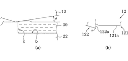
以上、本発明に係る微細構造体成形方法及び微細構造体成形金型について説明した。しかしながら、本発明は、上記実施形態に限定されない。例えば、本発明に係る微細構造体成形方法は、図4(a)に示す微細構造体成形金型によっても実施することができる。図4(a)において、塗膜30は、下型部22の微細構造を有するb面及びc面により形成される凹部に形成されるようになっている。そして、上型部12は傾斜角θをなして下型部22に当接するようになっている。
The microstructure forming method and the microstructure forming mold according to the present invention have been described above. However, the present invention is not limited to the above embodiment. For example, the microstructure forming method according to the present invention can also be implemented by a microstructure forming mold shown in FIG. In FIG. 4A, the
また、図1に示す上型部12に対して、上面型部121の121aの面と端面型部122の122aの面の接合部分に図4(b)に示すようなくさび状の凹部を設けた上型部12を用いる場合は、一の縁端部の端面の面積を大きくすることができ、その端面から次第に断面積が小さくなって一様な断面積の平面部に続く形態の微細構造体を成形することができる。このくさび状凹部は、図4(a)に示す微細構造体成形金型の底部に設けてもよい。
1 is provided with a wedge-shaped recess as shown in FIG. 4B at the joint between the
図1に示す微細構造体成形金型を使用して厚さ230μmのポリカーボネートからなる平板状の微細構造体を成形する成形試験を行った。成形試験は以下のように行った。上型部の端面型部は、h=230μmのものを使用した。弾性部材18Aは、厚み0.7mm、硬度50°(弾性率14.2MPa)のシリコンゴムを使用した。弾性部材18Bは、厚み0.5mm、硬度50°(弾性率14.2MPa)のシリコンゴムを使用した。塗膜は、吐出幅が104mmのTダイを使用してポリカーボネートの285℃の溶融樹脂を下型部に塗布することにより形成した。塗膜は厚さが240μm、端面型部との隙間δは1.8mmであった。上金型と下金型の設定温度は、195℃とし、195℃まで温度を上昇させた後にTダイで下型部にポリカーボネートの溶融樹脂を塗布した。なお、上型部及び下型部は、凹凸のない鏡面状態とした。良好な転写成形が行われると、得られた微細構造体は、その天面及び底面が極めて平滑で光沢面を有している。
A molding test was performed to mold a flat microstructure made of polycarbonate having a thickness of 230 μm using the microstructure molding mold shown in FIG. The molding test was conducted as follows. The end mold part of the upper mold part was h = 230 μm. As the
上記状態において、先ず、上金型を下降させて塗膜を3MPa(=押圧推力(N)÷平板状の微細構造体の投影面積(m2))の加圧力で押圧した。次に、3MPaの加圧力で押圧している最中に金型の冷却を始めるとともに、加圧力を0MPaまで徐々に低下させた。上金型の温度が135℃、下金型の温度が150℃まで低下したときに、金型を開いて転写成形された微細構造体を取り出した。 In the above state, first, the upper mold was lowered and the coating film was pressed with a pressure of 3 MPa (= pressing thrust (N) ÷ projected area (m 2 ) of the flat microstructure). Next, cooling of the mold was started while pressing at a pressure of 3 MPa, and the pressure was gradually reduced to 0 MPa. When the temperature of the upper mold was lowered to 135 ° C. and the temperature of the lower mold was lowered to 150 ° C., the mold was opened and the transferred microstructure was taken out.
また、上記成形試験に対する比較例として、弾性部材18A及び18Bがともに厚み0.5mm、硬度50°(弾性率14.2MPa)のシリコンゴムを使用した成形試験を行った。さらに、本発明における塗膜の押圧状況を調べるため、実施例1において上型部及び下型部に平板状の鏡面板を使用し、鏡面板同士を押圧したときの圧力分布を調べる加圧試験をおこなった。圧力分布の測定には富士フィルム社製のプレスケール低圧用(測定可能圧力2.5〜10MPa)を使用した。
In addition, as a comparative example for the above molding test, a molding test was conducted in which the
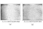
図5に加圧試験結果を示す。図5(a)は、弾性部材18Aを厚み0.6mm、硬度50°(弾性率14.2MPa)のシリコンゴム、弾性部材18Bを厚み0.5mm、硬度50°(弾性率14.2MPa)のシリコンゴムを使用したときの、上型部が水平から傾斜(下型部に対して傾斜)している場合の加圧試験結果を示す。図5(b)は弾性部材18A、18Bがともに厚み0.5mm、硬度50°(弾性率14.2MPa)のシリコンゴムを使用し、上型部が下型部に対して傾斜していない(水平である)場合の結果を示す。図5(a)を図5(b)と比較すると、図5(a)の場合は、押圧初期に一の縁端部側のみが当接するためこの周辺の押圧力が高くなっているが、最終的に上型部が当接部を中心に回転して、一の縁端部の反対側(紙面右側)も押圧され、全体的として均一に押圧されていることが分かる。
FIG. 5 shows the pressure test results. In FIG. 5 (a), the
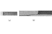
図6に、発明例と比較例の成形試験結果を示す。発明例は、一の縁端部にバリがないことが分かる。また、発明例の場合は、平面部(天面及び底面)ばかりでなく、一の縁端部も極めて平滑で光沢のある鏡面をしており、本発明によれば、平面部及び一の縁端部においても微細構造の高精度の転写成形が充分可能であることが分かる。 FIG. 6 shows the molding test results of the invention example and the comparative example. It can be seen that the inventive example has no burrs at one edge. In addition, in the case of the invention example, not only the flat portion (top and bottom surfaces) but also one edge portion has a very smooth and glossy mirror surface. According to the present invention, the flat portion and one edge It can be seen that highly accurate transfer molding with a fine structure is also possible at the end.
10 上金型
11 上母型
12 上型部
121 上面型部
122 端面型部
125 温度制御手段
15、15A、15B 断熱部材
18、18A、18B 弾性部材
20 下金型
21 下母型
22 下型部
225 温度制御手段
25 断熱部材
30 塗膜
10 Upper mold
11 Upper matrix
12 Upper mold part
121 Top mold part
122 End mold part
125 Temperature control means
15, 15A, 15B Thermal insulation member
18, 18A, 18B Elastic member
20 Lower mold
21 Lower matrix
22 Lower mold part
225 Temperature control means
25 Thermal insulation
30 coatings
Claims (11)
前記下金型に、平板状の塗膜を形成する段階と、
前記上金型を水平から傾斜させた状態でその下端の先端部を前記下金型に当接させた後、その当接部を中心に前記上金型が水平になるまで回転させるとともに押圧し、前記塗膜の平面部及び一の縁端部に前記微細構造の転写成形を行う微細構造体成形方法。 The coating film formed by applying the molten resin to the lower mold is pressed by the upper mold, and the fine structure is transferred to the flat portion and one edge portion of the coating film, and this is cooled and solidified. A method of forming a flat microstructure without a burr at the one edge, while having the microstructure at one edge and a plane part,
Forming a flat coating film on the lower mold; and
With the upper die tilted from the horizontal, the lower end of the tip is brought into contact with the lower die, and then the upper die is rotated and pressed around the contact portion until the upper die becomes horizontal. A fine structure molding method for performing transfer molding of the fine structure on a flat surface portion and one edge portion of the coating film.
上母型に弾性部材を介して保持される上型部が前記平面部の転写成形を行う上面型部と、前記一の縁端部の転写成形を行う端面型部とを有する上金型と、
前記上金型に対向する下金型を有し、
前記上金型は、前記弾性部材により水平から傾斜させた状態になるようになっている微細構造体成形金型。 The coating film formed by applying the molten resin to the lower mold is pressed by an upper mold having a fine structure, and the fine structure is transferred and molded on the flat portion and one edge portion of the coating film. A microstructure-molding mold for cooling and solidifying, and molding a planar microstructure having the microstructure on one edge with the plane portion,
An upper mold having an upper mold part that performs transfer molding of the flat surface part, and an end mold part that performs transfer molding of the one edge part, and an upper mold part held by an elastic member via an elastic member; ,
Having a lower mold facing the upper mold;
The upper mold is a microstructure forming mold configured to be inclined from the horizontal by the elastic member.
Priority Applications (1)
| Application Number | Priority Date | Filing Date | Title |
|---|---|---|---|
| JP2013031942A JP2014162012A (en) | 2013-02-21 | 2013-02-21 | Microstructure molding method and microstructure molding die |
Applications Claiming Priority (1)
| Application Number | Priority Date | Filing Date | Title |
|---|---|---|---|
| JP2013031942A JP2014162012A (en) | 2013-02-21 | 2013-02-21 | Microstructure molding method and microstructure molding die |
Publications (1)
| Publication Number | Publication Date |
|---|---|
| JP2014162012A true JP2014162012A (en) | 2014-09-08 |
Family
ID=51613121
Family Applications (1)
| Application Number | Title | Priority Date | Filing Date |
|---|---|---|---|
| JP2013031942A Pending JP2014162012A (en) | 2013-02-21 | 2013-02-21 | Microstructure molding method and microstructure molding die |
Country Status (1)
| Country | Link |
|---|---|
| JP (1) | JP2014162012A (en) |
Cited By (2)
| Publication number | Priority date | Publication date | Assignee | Title |
|---|---|---|---|---|
| JP2016221838A (en) * | 2015-05-29 | 2016-12-28 | 株式会社日本製鋼所 | Resin molding method, mold used therefor, and resin filling jig |
| JP2016221785A (en) * | 2015-05-28 | 2016-12-28 | 株式会社日本製鋼所 | Resin molding die and resin molding method using the same |
Citations (7)
| Publication number | Priority date | Publication date | Assignee | Title |
|---|---|---|---|---|
| JPS5836417A (en) * | 1981-08-27 | 1983-03-03 | Matsushita Electric Ind Co Ltd | Manufacture of information carrier |
| JPH10510770A (en) * | 1994-12-19 | 1998-10-20 | サン−ゴバン ビトラージュ | How to finish extruded seals on the sheet on the fly |
| JP2004358857A (en) * | 2003-06-06 | 2004-12-24 | Meiki Co Ltd | Apparatus for forming resin formed product having fine uneven surface |
| JP2006007755A (en) * | 2004-05-28 | 2006-01-12 | Komatsu Ltd | Thermal transfer press |
| JP2007106002A (en) * | 2005-10-13 | 2007-04-26 | Matsushita Electric Works Ltd | Fine shape molding method |
| JP2010089327A (en) * | 2008-10-07 | 2010-04-22 | Japan Steel Works Ltd:The | Molding device and method of manufacturing molding using the same |
| JP2012245745A (en) * | 2011-05-30 | 2012-12-13 | Japan Steel Works Ltd:The | Melt fine-transfer molding method, and melt fine-transfer molding device |
-
2013
- 2013-02-21 JP JP2013031942A patent/JP2014162012A/en active Pending
Patent Citations (7)
| Publication number | Priority date | Publication date | Assignee | Title |
|---|---|---|---|---|
| JPS5836417A (en) * | 1981-08-27 | 1983-03-03 | Matsushita Electric Ind Co Ltd | Manufacture of information carrier |
| JPH10510770A (en) * | 1994-12-19 | 1998-10-20 | サン−ゴバン ビトラージュ | How to finish extruded seals on the sheet on the fly |
| JP2004358857A (en) * | 2003-06-06 | 2004-12-24 | Meiki Co Ltd | Apparatus for forming resin formed product having fine uneven surface |
| JP2006007755A (en) * | 2004-05-28 | 2006-01-12 | Komatsu Ltd | Thermal transfer press |
| JP2007106002A (en) * | 2005-10-13 | 2007-04-26 | Matsushita Electric Works Ltd | Fine shape molding method |
| JP2010089327A (en) * | 2008-10-07 | 2010-04-22 | Japan Steel Works Ltd:The | Molding device and method of manufacturing molding using the same |
| JP2012245745A (en) * | 2011-05-30 | 2012-12-13 | Japan Steel Works Ltd:The | Melt fine-transfer molding method, and melt fine-transfer molding device |
Cited By (2)
| Publication number | Priority date | Publication date | Assignee | Title |
|---|---|---|---|---|
| JP2016221785A (en) * | 2015-05-28 | 2016-12-28 | 株式会社日本製鋼所 | Resin molding die and resin molding method using the same |
| JP2016221838A (en) * | 2015-05-29 | 2016-12-28 | 株式会社日本製鋼所 | Resin molding method, mold used therefor, and resin filling jig |
Similar Documents
| Publication | Publication Date | Title |
|---|---|---|
| JP3857703B2 (en) | Manufacturing method and manufacturing apparatus of molded body | |
| JPWO2012086385A1 (en) | Manufacturing method of fine structure | |
| JP6108916B2 (en) | Molded product manufacturing method and molding die | |
| JP2014162012A (en) | Microstructure molding method and microstructure molding die | |
| JP5754749B2 (en) | Microstructure forming method | |
| EP0536872B1 (en) | Roll stamper for forming a base for information recording medium and apparatus using the roll stamper | |
| JP4699492B2 (en) | Molded body manufacturing apparatus and manufacturing method | |
| CN100532070C (en) | Device and method for manufacturing plate with embossing on surface | |
| JP2009172794A (en) | Manufacturing method of resin sheet | |
| US10369728B2 (en) | Optical element and method for manufacturing optical element | |
| JP3686251B2 (en) | Molding method of resin molded product and mold used for the method | |
| EP2596938A1 (en) | Pattern transfer medium manufacturing apparatus, pattern transfer manufacturing method, disc-shaped pattern transfer medium, and pattern transfer medium | |
| US11801626B2 (en) | Resin part and its manufacturing method | |
| JP4224052B2 (en) | Molded body manufacturing equipment | |
| US20090261489A1 (en) | Method for making lenses | |
| JP4224048B2 (en) | Molded body manufacturing apparatus and manufacturing method | |
| CN100519139C (en) | Forming method of optical disk substrate and blue-ray optical disk | |
| CN1669768A (en) | Die device for forming optical disk substrate | |
| JPH10235682A (en) | Injection molding equipment | |
| TWI445615B (en) | Press molding method for making lens array | |
| KR101625374B1 (en) | Method For Manufacturing Light Guide Plate | |
| EP4079481A1 (en) | Method and apparatus for adjusting recess depth of a mold insert | |
| JP4083446B2 (en) | Laminated optical recording medium | |
| JP2003154565A (en) | Manufacturing method of optical disk substrate | |
| JP3875807B2 (en) | Molding method of molded products |
Legal Events
| Date | Code | Title | Description |
|---|---|---|---|
| A131 | Notification of reasons for refusal |
Free format text: JAPANESE INTERMEDIATE CODE: A131 Effective date: 20140926 |
|
| A02 | Decision of refusal |
Free format text: JAPANESE INTERMEDIATE CODE: A02 Effective date: 20150514 |