JP2014190847A - Gas sensor - Google Patents
Gas sensor Download PDFInfo
- Publication number
- JP2014190847A JP2014190847A JP2013066814A JP2013066814A JP2014190847A JP 2014190847 A JP2014190847 A JP 2014190847A JP 2013066814 A JP2013066814 A JP 2013066814A JP 2013066814 A JP2013066814 A JP 2013066814A JP 2014190847 A JP2014190847 A JP 2014190847A
- Authority
- JP
- Japan
- Prior art keywords
- gas
- heating resistor
- gas sensor
- metal layer
- substrate
- Prior art date
- Legal status (The legal status is an assumption and is not a legal conclusion. Google has not performed a legal analysis and makes no representation as to the accuracy of the status listed.)
- Granted
Links
Images


Landscapes
- Investigating Or Analyzing Materials By The Use Of Electric Means (AREA)
Abstract
【課題】熱伝導式ガスセンサにおける発熱抵抗体から被検出ガスへの熱伝導率を高め、被検出ガスの検出精度を向上させたガスセンサを提供する。
【解決手段】基板61に形成された開口部62を覆うように当該基板に設けられた薄膜部と、薄膜部の内部に設けられ、自身の温度変化により抵抗値が変化するヒータ71と、を備えた熱伝導式のガスセンサ1であって、薄膜部のうち、ヒータの形成領域71Rの表面の少なくとも一部に凹凸を有する金属層75が形成されている。
【選択図】 図3The present invention provides a gas sensor in which the thermal conductivity from a heating resistor to a gas to be detected in a heat conduction gas sensor is increased, and the detection accuracy of the gas to be detected is improved.
SOLUTION: A thin film portion provided on a substrate so as to cover an opening 62 formed in the substrate 61, and a heater 71 provided in the thin film portion, the resistance value of which changes with its own temperature change, are provided. In the heat-conducting gas sensor 1 provided, a metal layer 75 having irregularities is formed on at least a part of the surface of the heater forming region 71R in the thin film portion.
[Selection] Figure 3
Description
本発明は、被検出雰囲気中に存在する可燃性ガス等のガス濃度を検出するガスセンサに関する。 The present invention relates to a gas sensor that detects a gas concentration of a combustible gas or the like present in an atmosphere to be detected.
近年、環境・自然保護などの社会的要求から、高効率で、クリーンなエネルギー源として燃料電池の研究が活発に行われている。その中で、低温作動、高出力密度等の利点により、家庭用、車載用などのエネルギー源として固体高分子型燃料電池(PEFC)や水素内燃機関が期待されている。これらのシステムでは、例えば、可燃性ガスである水素を燃料としているため、ガス漏れの検知が重要な課題の一つとして挙げられている。 In recent years, research on fuel cells has been actively conducted as a high-efficiency, clean energy source due to social demands such as environmental protection and nature conservation. Among them, solid polymer fuel cells (PEFCs) and hydrogen internal combustion engines are expected as energy sources for home use and on-vehicle use due to advantages such as low temperature operation and high output density. In these systems, for example, hydrogen, which is a flammable gas, is used as a fuel, so detection of gas leakage is cited as one of the important issues.
この種の被検出雰囲気中に存在する可燃性ガスのガス濃度を検出するガスセンサとして、被検出雰囲気内にガス検出素子を配置し、このガス検出素子に、自身の温度変化(発熱)により抵抗値が変化する発熱抵抗体を備えた熱伝導式ガスセンサが知られている(例えば、特許文献1、2参照)。具体的には、このガスセンサでは、発熱抵抗体に通電されて発熱抵抗体が発熱した際に可燃性ガスへの熱伝導(気体熱伝導)が生じる。そのため、ガス検出素子の温度を一定の温度に制御する場合、熱伝導によって発熱抵抗体の温度が変化するとともに抵抗値が変化するため、その変化量に基づき、被検出ガスを検出することができる。
そして、上記ガス検出素子はMEMSの技術を用いて作製されており、基板上にダイヤフラムを形成する絶縁層を設け、この絶縁層に発熱抵抗体を配置させる構成を採っている。これにより、発熱抵抗体から基板への熱逃げがダイヤフラム部分で少なくなるので、発熱抵抗体の熱が被検出ガスへ伝わり易くなる。
As a gas sensor that detects the gas concentration of the combustible gas present in this type of atmosphere to be detected, a gas detection element is arranged in the atmosphere to be detected, and this gas detection element has a resistance value due to its own temperature change (heat generation). There is known a heat conduction type gas sensor provided with a heating resistor in which the temperature changes (see, for example, Patent Documents 1 and 2). Specifically, in this gas sensor, when the heating resistor is energized and the heating resistor generates heat, heat conduction to the combustible gas (gas heat conduction) occurs. Therefore, when the temperature of the gas detection element is controlled to a constant temperature, the temperature of the heating resistor changes due to heat conduction and the resistance value changes, so that the gas to be detected can be detected based on the change amount. .
The gas detection element is manufactured using a MEMS technique, and has a configuration in which an insulating layer for forming a diaphragm is provided on a substrate and a heating resistor is disposed on the insulating layer. As a result, heat escape from the heating resistor to the substrate is reduced at the diaphragm portion, so that the heat of the heating resistor is easily transferred to the gas to be detected.
しかしながら、上記したダイヤフラムは、絶縁層と半導体基板との接触部分からの熱逃げを低減したものに過ぎず、被検出ガスの検出精度をさらに向上させるためには、発熱抵抗体から可燃性ガスへの熱伝導率(気体熱伝導の度合い)を積極的に高める必要がある。
すなわち、本発明は、熱伝導式ガスセンサにおける発熱抵抗体から被検出ガスへの熱伝導率を高め、被検出ガスの検出精度を向上させたガスセンサの提供を目的とする。
However, the diaphragm described above is merely a reduction in heat escape from the contact portion between the insulating layer and the semiconductor substrate, and in order to further improve the detection accuracy of the gas to be detected, the heating resistor is changed to a combustible gas. It is necessary to positively increase the thermal conductivity (degree of gas thermal conduction).
That is, an object of the present invention is to provide a gas sensor in which the thermal conductivity from the heating resistor to the gas to be detected in the heat conduction type gas sensor is increased and the detection accuracy of the gas to be detected is improved.
上記課題を解決するため、本発明のガスセンサは、基板に形成された開口部を覆うように当該基板に設けられた薄膜部と、前記薄膜部の内部に設けられ、自身の温度変化により抵抗値が変化するヒータと、を備えた熱伝導式のガスセンサであって、前記薄膜部のうち、前記ヒータの形成領域の表面の少なくとも一部に凹凸を有する金属層が形成されている。
このガスセンサによれば、発熱抵抗体から、凹凸が設けられたことで表面積が平面の構成よりも増加した金属層を介して被検出ガスへ熱が伝わり易くなり、発熱抵抗体から被検出ガスへの熱伝導率を高め、被検出ガスの検出精度を向上させることができる。又、発熱抵抗体から金属層側への熱の伝達経路が形成されるので、薄膜部と基板との接触部分からの熱逃げが少なくなる。
In order to solve the above problems, the gas sensor of the present invention is provided with a thin film portion provided on the substrate so as to cover an opening formed on the substrate, and the resistance value due to its own temperature change. A heat conduction type gas sensor including a heater in which a metal layer having irregularities is formed on at least a part of the surface of the heater formation region in the thin film portion.
According to this gas sensor, heat is easily transferred from the heating resistor to the gas to be detected through the metal layer having the surface area increased from that of the planar structure due to the provision of the unevenness, and from the heating resistor to the gas to be detected. The thermal conductivity of the gas can be increased, and the detection accuracy of the gas to be detected can be improved. Further, since a heat transfer path from the heating resistor to the metal layer side is formed, heat escape from the contact portion between the thin film portion and the substrate is reduced.
前記金属層は、前記薄膜部のうち、前記開口部の周縁よりも内側の領域に形成されていることが好ましい。
このガスセンサによれば、金属層の熱が基板側へ逃げ難くなるため、発熱抵抗体から被検出ガスへの熱伝導を低下させることを抑制できる。
The metal layer is preferably formed in a region inside the thin film portion with respect to the periphery of the opening.
According to this gas sensor, it becomes difficult for the heat of the metal layer to escape to the substrate side, so that it is possible to suppress a decrease in heat conduction from the heating resistor to the gas to be detected.
前記金属層は、Al,Cu,Au又はこれらの合金をスパッタ成膜してなることが好ましい。
このガスセンサによれば、金属層に凹凸を容易に形成することができる。また、Al,Cu,Au又はこれらの合金から金属層を形成することで、金属層自身の熱伝導率が高く、凹凸を設けた構成と相俟って、発熱抵抗体から被検出ガスへの熱伝導の度合いを高めることができる。
The metal layer is preferably formed by sputtering Al, Cu, Au, or an alloy thereof.
According to this gas sensor, irregularities can be easily formed in the metal layer. In addition, by forming the metal layer from Al, Cu, Au or an alloy thereof, the metal layer itself has a high thermal conductivity, and in combination with the structure provided with unevenness, the heating resistor to the gas to be detected The degree of heat conduction can be increased.
前記ガスセンサは水素ガスを検出対象とすると、実用的であるので好ましい。 The gas sensor is preferable because it is practical to detect hydrogen gas.
この発明によれば、熱伝導式ガスセンサにおける発熱抵抗体から被検出ガスへの熱伝導率を高め、被検出ガスの検出精度を向上させることができる。 According to this invention, the thermal conductivity from the heating resistor to the gas to be detected in the heat conduction type gas sensor can be increased, and the detection accuracy of the gas to be detected can be improved.
以下に、本発明の実施形態を図面と共に説明する。
図1は、本発明が適用されたガスセンサ1の全体構成図である。図2は、ガスセンサ1の主要部となるガス検出素子60の構成を示す平面図(但し、内部構成も一部示す)であり、図4が図2におけるA−A線に沿ったガス検出素子の断面図である。
Embodiments of the present invention will be described below with reference to the drawings.
FIG. 1 is an overall configuration diagram of a gas sensor 1 to which the present invention is applied. FIG. 2 is a plan view showing the configuration of the
[全体構成]
ガスセンサ1は、熱伝導式のガス検出素子60を用いて、可燃性ガスの濃度を検出するものであり、例えば、燃料電池自動車の客室内に設置され、水素の漏れを検出する目的等に用いられる。
[overall structure]
The gas sensor 1 detects the concentration of combustible gas using a heat-conducting
図1に示すように、ガスセンサ1は、ガス検出素子60(図2、図3参照)と、ガス検出素子60を駆動制御する制御回路90とを備えている。又、制御回路90は、ガス検出回路91、及び温度測定回路93を備えている。なお、制御回路90(但し、後述する発熱抵抗体71および測温抵抗体80を除く),マイコン94は単一の回路基板上に構成され、この回路基板とは別体にガス検出素子60は構成されている。
ガス検出回路91は、ガス検出素子60に備えられた発熱抵抗体71と、固定抵抗95,96,97とによって構成されるホイートストーンブリッジ911、及び、ホイートストーンブリッジ911から得られる電位差を増幅するオペアンプ912を備えている。
発熱抵抗体71として、自身の温度の上昇に伴い抵抗値が上昇する抵抗体を用いた場合、このオペアンプ912は、発熱抵抗体71の温度が所定の温度に保たれるように、発熱抵抗体71の温度が上昇した場合には出力する電圧を低くし、発熱抵抗体71の温度が下降した場合には出力する電圧を高くするように作動する。
As shown in FIG. 1, the gas sensor 1 includes a gas detection element 60 (see FIGS. 2 and 3) and a
The
When a resistor whose resistance value increases as its temperature rises is used as the
そして、このオペアンプ912の出力は、ホイートストーンブリッジ911に接続されているので、発熱抵抗体71の温度が所定の温度より上昇すると、発熱抵抗体71の温度を下げるためにオペアンプ912から出力される電圧は低くなり、ホイートストーンブリッジ911に印加される電圧が低下する。このときの、ホイートストーンブリッジ911の端部を構成する電極85の電圧はガス検出回路91の出力としてマイコン94により検出され、マイコン94により検出された出力値は、被検出ガスに含まれ可燃性ガスを検出するための演算処理に供される。
温度測定回路93は、ガス検出素子60に備えられた測温抵抗体80(後述する)と、固定抵抗101,102,103によって構成されるホイートストーンブリッジ931と、ホイートストーンブリッジ931から得られる電位差を増幅するオペアンプ933とを備えている。このオペアンプ933の出力はマイコン94により検出され、マイコン94により検出された出力値は、被検出ガスの温度を測定するのに用いられ、さらに、被検出ガスに含まれ可燃性ガスを検出するための演算処理に供される。
Since the output of the
The
以上のような構成を有する制御回路90の出力値に基づき、マイコン94により実行される可燃性ガスの濃度を演算する処理は、次のようなものである。まず、マイコン94が備えるCPU(図示せず)は、同じくマイコン94が備える記憶装置(図示せず)に記憶されたプログラムに基づき、ガス検出回路91の出力値から、可燃性ガス濃度にほぼ比例した第1の算出値を算出する。この第1の算出値は、ガスセンサ1の検出空間の雰囲気温度変化に依存して変化するため、別途にCPUに入力される温度測定回路93からの出力に基づき、第1の算出値を補正した第2の算出値を算出する。さらに、マイコン94は、そのマイコン94の記憶装置(図示せず)に記憶された第2の算出値と可燃性ガスの濃度との関係に基づき、被検出ガス中に含まれる可燃性ガスの濃度を算出し、外部回路に出力する。このように、第1の算出値(ガス検出回路91の出力値)を温度測定回路93の出力に基づき補正しているので、精度よく可燃性ガスを検出できる。尚、可燃性ガスの濃度を演算する処理は、上記のものに限られず、公知の手段を適宜用いれば良い。
The processing for calculating the concentration of the combustible gas executed by the
[ガス検出素子]
次に、ガス検出素子60の構成について説明する。図2はガス検出素子60の平面図を示し、図3は図2のA−A矢視断面図を示す。尚、図2において、紙面の左右方向をその平面図の左右方向とする。また、図3において、紙面の上下方向をその断面図の上下方向とする。
図2に示すように、ガス検出素子60は、平板形状(平面視四角形状)をなし、その表面の四隅にそれぞれ電極85、86、88、89が形成され、他方の面(裏面)の中心付近に、表面に向かって凹む平面視矩形の凹部62が形成されている。
又、図3に示すように、ガス検出素子60は、シリコン半導体からなる基板61を備えるとともに、基板61の上下両側に絶縁層(上側絶縁層67、下側絶縁層66)を備えている。上側絶縁層67は、基板61の表面に形成されており、一方、下側絶縁層66は、基板61の裏面に形成されている。上側絶縁層67は、基板61の表面に形成される第1絶縁層68と、絶縁層68の表面に形成される絶縁保護層69と、絶縁保護層69の表面に形成された第2絶縁層64から構成される。
そして、上側絶縁層67が部分的(平面から見てほぼ正方形)に露出するように基板61の一部を除去することで、図2に示すような凹部(基板61の開口部)62が形成されたダイヤフラム構造をなしている。上側絶縁層67のうち、凹部62を形成する領域(換言すれば、基板61に形成された開口部を塞ぐ隔壁部分)が特許請求の範囲の「薄膜部」に相当する。
[Gas detection element]
Next, the configuration of the
As shown in FIG. 2, the
As shown in FIG. 3, the
Then, a part of the
上側絶縁層67のうち凹部62に対応する領域(薄膜部)には、渦巻き状にパターン形成された発熱抵抗体(特許請求の範囲の「ヒータ」)71が埋設されている。
発熱抵抗体71は、被検出ガスの温度(詳細には、可燃性ガスへの気体熱伝導)に伴う自身の温度変化により抵抗値が変化する抵抗体である。発熱抵抗体71は、温度抵抗係数が大きい導電性材料で構成され、本実施形態では白金(Pt)で形成されている。可燃性ガスとしての水素ガスを検出する場合、水素ガスへの熱伝導によって発熱抵抗体71から奪われる熱量の大きさは、水素ガス濃度に応じた大きさとなる。このことから、発熱抵抗体71における抵抗値の変化に基づいて、水素ガス濃度を検出することが可能となる。
そして、上側絶縁層67のうち、凹部62に対応する領域(薄膜部)の内部に発熱抵抗体71を設けることにより、発熱抵抗体71が周囲から断熱されるため、短時間にて昇温又は降温する。このため、ガス検出素子60の熱容量を小さくすることができる。
In a region (thin film portion) corresponding to the
The
Then, by providing the
なお、上側絶縁層67は、単一の材料で形成されてもよいし、異なる材料を用いて複数層を成すように形成されてもよい。本実施形態では上側絶縁層67を構成する複数層のうち、第1絶縁層68が窒化珪素(Si3N4)からなり、絶縁保護層69が酸化ケイ素(SiO2)からなり、第2絶縁層64が窒化珪素(Si3N4)からなっていて、発熱抵抗体71は絶縁保護層69内に埋設されている。
又、ガス検出素子60は、縦横ともに数mm(例えば3mm×3mm)程度の大きさであり、例えば、シリコン半導体基板を用いたマイクロマシニング技術(マイクロマシニング加工)により製造される。
Note that the upper insulating
The
図2に戻り、発熱抵抗体71の左端は、発熱抵抗体71が形成された平面と同じ平面に埋設された配線713および配線膜711(図3)を介して電極85に接続されている。又、発熱抵抗体71の右端は、発熱抵抗体71が形成された平面と同じ平面に埋設された配線714および配線膜712(図3)を介してグランド電極86に接続されている。電極85及びグランド電極86は、発熱抵抗体71に接続される配線の引き出し部位であり、コンタクトホール84(図3)を介して露出し、例えば、アルミニウム(Al)又は金(Au)で形成されている。
Returning to FIG. 2, the left end of the
測温抵抗体80は、ガスセンサ1の検出空間内に存在する被検出ガスの温度を検出するためのものであり、ガス検出素子60の上辺(一辺)に沿って、上側絶縁層67と保護層64との間に埋設されている。測温抵抗体80は、抵抗値が温度に比例して変化(本実施形態では、温度の上昇に伴って抵抗値が増大)する導電性材料で構成され、本実施形態では白金(Pt)で形成されている。
測温抵抗体80は、測温抵抗体80が形成された平面と同じ平面に埋設された配線膜(図示せず)を介して電極88及びグランド電極89に接続されている。電極88及びグランド電極89は、コンタクトホール(図示せず)を介して露出し、例えば、アルミニウム(Al)又は金(Au)で形成されている。
The
The
さらに、図3に示すように、発熱抵抗体71の形成領域における第2絶縁層64の表面に、凹凸(粗面)を有する金属層75が形成されている。このようにすると、発熱抵抗体71から、凹凸の形成によって表面積が増大した金属層75を介して被検出ガスへ熱が伝わり易くなり、発熱抵抗体71から被検出ガスへの熱伝導率(気体熱伝導の度合い)が高まり、被検出ガスの検出精度が向上する。又、発熱抵抗体71から金属層75側への熱の伝達経路が形成されるので、薄膜部(上側絶縁層67)と基板61との接触部分からの熱逃げが少なくなる。
ガス検出素子60の平面方向に見て、発熱抵抗体71の形成領域71Rよりも内側に金属層75を設けてもよいし、形成領域71Rより外側へ金属層75がはみ出してもよいが、熱伝導率を高めるためには、図3に示すように形成領域71Rと丁度重なるように金属層75を設けることが好ましい。又、上側絶縁層67のうち、ガス検出素子60の平面方向に見て、凹部(基板61の開口部)62よりも内側の領域に、金属層75が形成されていることが好ましい。その理由は、ガス検出素子60の平面方向に見て、金属層75の一部が基板61の開口部の周縁(薄膜部の形成領域端)に対応する位置にまで形成されているか、基板の周縁(薄膜部の形成領域端)より外側にまではみ出して形成されると、基板61側へ金属層75の熱が逃げ、発熱抵抗体71から被検出ガスへの熱伝導が少なくなるおそれがあるからである。
金属層75は、金属単体であってもよく、合金であってもよい。金属層75が熱伝導率の高いAl,Cu,Au又はこれらの合金からなることが好ましい。特に、金属層75がAl,Cu,Au、又はこれらの合金をスパッタ成膜してなることが好ましい。
Further, as shown in FIG. 3, a
When viewed in the plane direction of the
The
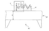
又、図4に示すように、金属層75の断面をレーザ顕微鏡(倍率100倍)で観察したとき、0.128mm×0.096mmの1視野S中で最も高いピークh1からh10までの10点の平均高さが、上側絶縁層67のうち凹部62(基板61の開口部)に対応する領域(薄膜部)の厚さDの1/2以上であると、発熱抵抗体71から被検出ガスへの熱伝導率が高くなるので好ましい。ピークh1からh10までの10点の平均高さTを規定する理由は、金属層75のうち、高さの高い凸部から優先的に被検出ガスへ熱が伝わるので、これら凸部の高さを反映させるためである。なお、図4では、理解を容易にするため、最も高いピークh1から4番目のピークh4までを特定し、模式的に示している。
又、各ピークh1〜h10の高さは、第2絶縁層64(薄膜部)の最表面からの高さである。
As shown in FIG. 4, when the cross section of the
The heights of the peaks h1 to h10 are the heights from the outermost surface of the second insulating layer 64 (thin film portion).
金属層75の製造方法としては、金属層75を構成する金属を含むペーストを印刷したり、メッキする方法(厚膜法)や、スパッタ(スパッタリング法)等の薄膜法が挙げられる。金属層75の表面を凹凸にする方法としては、スパッタ時の雰囲気ガス中に金属層75を構成する材料と異なる不純物を存在させ、金属層75をデンドライト状に異常成長させる方法が挙げられる。例えば、Arガス中に窒素を混合させた雰囲気が例示される。
As a manufacturing method of the
次に、図5、図6を参照し、ガス検出素子60の製造工程について説明する。なお、下記の各被膜の組成や厚みは例示に過ぎない。
第1絶縁層68、下側絶縁層66、絶縁保護層69の一部の形成工程(図5(a))
シリコン半導体からなる基板61を準備し、この基板61を洗浄した上で基板61の上下両面に減圧CVD法により、窒化珪素膜(Si3N4膜)をそれぞれ200nmの厚さ形成する。これにより、基板61の上側の窒化珪素膜が第1絶縁層68として形成され、一方、基板61の下側の窒化珪素膜が下側絶縁層66として形成される。
次に、絶縁層68の表面上に、酸化珪素層(SiO2層)からなる絶縁保護層69の一部をなす下側絶縁保護層69aをプラズマCVD法により、100nmの厚さにて形成する。
Next, the manufacturing process of the
Step of forming a part of the first insulating
A
Next, on the surface of the insulating
発熱抵抗体71及び配線膜711,712の形成工程(図5(b))
次に、温度300℃の雰囲気内において、タンタル膜(Ta膜)を20nmの厚さにて下側絶縁保護層69aの表面にスパッタ法により形成し、ついで、白金膜(Pt膜)を150nmの厚さにてタンタル膜上にスパッタ法により積層状に形成する。その後、フォトリソグラフィ処理にて、タンタル膜、及び白金膜のうち発熱抵抗体71及び配線膜711,712に対する対応部以外の部位を、エッチングにより除去する。これにより、発熱抵抗体71及び配線膜711,712が、下側絶縁保護層69aの表面上に形成される。尚、配線膜711,712及び発熱抵抗体71の抵抗温度係数は、約2500[ppm/℃]である。この工程において、測温抵抗体80についても、発熱抵抗体71と同様の手法により、下側絶縁保護層69aの表面上に形成する。
Step of forming the
Next, in an atmosphere at a temperature of 300 ° C., a tantalum film (Ta film) is formed by sputtering on the surface of the lower insulating
絶縁保護層69全体、及び第2絶縁層64の形成工程(図5(c))
次に、各発熱抵抗体71及び配線膜711,712を覆うようにして下側絶縁保護層69aの表面上に、同じ組成の上側絶縁保護層69bをプラズマCVD法により、100nmの厚さにて形成する。各発熱抵抗体71及び配線膜711,712は、下側絶縁保護層69a及び上側絶縁保護層69bの間に埋設され、下側絶縁保護層69a及び上側絶縁保護層69bは一体の層である絶縁保護層69を構成する。
さらに絶縁保護層69上に、窒化珪素層(Si3N4層)からなる第2絶縁層64を、減圧CVD法により、200nmの厚さにて積層状に形成する。
Step of forming the entire insulating
Next, an upper insulating
Further, a second insulating
コンタクトホールの形成工程(図6(d))
ついで、絶縁保護層69及び第2絶縁層64の積層のうち配線膜711,712に対応する各部位を、フォトリソグラフィ処理のもとエッチングにより除去する。これにより、コンタクトホール84が配線膜711,712上をに形成される。また、同様のエッチングにより、測温抵抗体80用のコンタクトホール(図示せず)を形成する。
Contact hole formation process (FIG. 6D)
Next, each part corresponding to the
電極85,86の形成工程(図6(e))
上述のように第2絶縁層64を形成した後、クロム膜(Cr膜)を20nmの厚さにて第2絶縁層64上にスパッタ法により層状に形成し、ついで、このクロム膜上に、金膜(Au膜)を400nmの厚さにてスパッタ法により積層状に形成する。
その後、このように積層した金膜及びクロム膜からなる電極層のうち各コンタクトホール84に対する対応部以外の部位を、フォトリソグラフィ処理のもとエッチングにより除去する。これにより、電極85,86が、各コンタクトホール84に対応して形成される。また、この工程の際に、電極88及びグランド電極89についても、図示しないコンタクトホールに対応して形成される。
Step of forming
After forming the second insulating
Thereafter, the portions other than the corresponding portions corresponding to the contact holes 84 in the electrode layer composed of the gold film and the chromium film laminated in this manner are removed by etching under a photolithography process. As a result,
ダイヤフラム62の形成工程(図6(f))
上述のように電極85,86を形成した後、下側絶縁層66のうち発熱抵抗体71に対応する各部位を、エッチングにより除去し、ついで、この除去部位に対応する基板61の各部位を水酸化テトラメチルアンモニウムを用いてエッチングにより除去して、絶縁層68のうち発熱抵抗体71に対応する部位を外方に露呈させる。これにより、基板61に開口部が形成され、凹部62が、基板61及び下側絶縁層66のうち発熱抵抗体71に対応する部位に形成される。
Formation process of the diaphragm 62 (FIG. 6F)
After the
金属層75の形成工程(図6(g))
第2絶縁層64、電極85、86、電極88及びグランド電極89の全体を覆うように、酸化珪素層(SiO2層)からなる電極保護層をプラズマCVD法により形成する。この電極保護層は、金属層75の形成にあたって各電極85、86、88、89を保護するためのものである。
次に、電極保護層の表面に、Arガス中に窒素を混合させた雰囲気中でAlをスパッタ形成した後、発熱抵抗体71に対応する部分を残してエッチングにより除去する。Arガス中に混合させた窒素により、金属層75がデンドライト状に異常成長し、その表面が凹凸(粗面)になる。
最後に、電極保護層をエッチングにより除去し、ガス検出素子60が完成する。
Step of forming metal layer 75 (FIG. 6G)
An electrode protective layer made of a silicon oxide layer (SiO 2 layer) is formed by plasma CVD so as to cover the second insulating
Next, Al is sputter-formed on the surface of the electrode protective layer in an atmosphere in which nitrogen is mixed in Ar gas, and then removed by etching leaving a portion corresponding to the
Finally, the electrode protection layer is removed by etching, and the
本発明は上記実施形態に限定されず、本発明の思想と範囲に含まれる様々な変形及び均等物に及ぶことはいうまでもない。例えば、上記実施形態では、水素ガスを検出する場合について説明したが、本発明のガスセンサは他の種類の可燃性ガスも検出可能である。また、上記実施形態では、金属層75を第2絶縁層64の表面に直接形成したが、第2絶縁層64上に当該第2絶縁層64を保護するための緻密な(ガス不透過性の)絶縁保護層(例えば、アルミナから形成される絶縁保護層)を形成し、その絶縁保護層上に金属層75を形成するようにしてもよい。
It goes without saying that the present invention is not limited to the above-described embodiment, but extends to various modifications and equivalents included in the spirit and scope of the present invention. For example, although the case where hydrogen gas is detected has been described in the above embodiment, the gas sensor of the present invention can also detect other types of combustible gases. In the above embodiment, the
1 ガスセンサ
61 基板
62 凹部(基板の開口部)
71 ヒータ(発熱抵抗体)
71R ヒータの形成領域
75 金属層
1
71 Heater (heating resistor)
71R
Claims (4)
前記薄膜部の内部に設けられ、自身の温度変化により抵抗値が変化するヒータと、を備えた熱伝導式のガスセンサであって、
前記薄膜部のうち、前記ヒータの形成領域の表面の少なくとも一部に凹凸を有する金属層が形成されているガスセンサ。 A thin film portion provided on the substrate so as to cover the opening formed in the substrate;
A heat conduction type gas sensor comprising a heater provided inside the thin film portion and having a resistance value that changes due to a temperature change of the thin film portion;
The gas sensor in which the metal layer which has an unevenness | corrugation is formed in at least one part of the surface of the formation area of the said heater among the said thin film parts.
Priority Applications (1)
| Application Number | Priority Date | Filing Date | Title |
|---|---|---|---|
| JP2013066814A JP6255162B2 (en) | 2013-03-27 | 2013-03-27 | Manufacturing method of gas sensor |
Applications Claiming Priority (1)
| Application Number | Priority Date | Filing Date | Title |
|---|---|---|---|
| JP2013066814A JP6255162B2 (en) | 2013-03-27 | 2013-03-27 | Manufacturing method of gas sensor |
Publications (2)
| Publication Number | Publication Date |
|---|---|
| JP2014190847A true JP2014190847A (en) | 2014-10-06 |
| JP6255162B2 JP6255162B2 (en) | 2017-12-27 |
Family
ID=51837231
Family Applications (1)
| Application Number | Title | Priority Date | Filing Date |
|---|---|---|---|
| JP2013066814A Active JP6255162B2 (en) | 2013-03-27 | 2013-03-27 | Manufacturing method of gas sensor |
Country Status (1)
| Country | Link |
|---|---|
| JP (1) | JP6255162B2 (en) |
Cited By (2)
| Publication number | Priority date | Publication date | Assignee | Title |
|---|---|---|---|---|
| CN118501216A (en) * | 2024-06-17 | 2024-08-16 | 海森赛尔(佛山)科技有限公司 | Chip structure, thermal conductivity type hydrogen sensor and manufacturing method thereof |
| CN118549496A (en) * | 2024-03-21 | 2024-08-27 | 海森赛尔(佛山)科技有限公司 | Thermal conductance type gas sensor and preparation method thereof |
Citations (9)
| Publication number | Priority date | Publication date | Assignee | Title |
|---|---|---|---|---|
| JPH116810A (en) * | 1997-06-18 | 1999-01-12 | Yazaki Corp | Gas sensor, contact combustion type gas sensor, and manufacturing method |
| JPH11241935A (en) * | 1998-02-25 | 1999-09-07 | Tokin Corp | Micro sensor |
| JP2004504598A (en) * | 2000-07-19 | 2004-02-12 | エルジー エレクトロニクス インコーポレーテッド | Absolute humidity sensor |
| JP2004177346A (en) * | 2002-11-28 | 2004-06-24 | Ngk Spark Plug Co Ltd | Gas sensor |
| JP2005300452A (en) * | 2004-04-15 | 2005-10-27 | Matsushita Electric Ind Co Ltd | Gas sensor, fuel cell system using the same, and automobile |
| US20080101434A1 (en) * | 2001-07-16 | 2008-05-01 | Horovitz Michael L | Sensor device and method for qualitative and quantitative analysis of gas phase substances |
| JP2010096727A (en) * | 2008-10-20 | 2010-04-30 | Ngk Spark Plug Co Ltd | Gas detector |
| JP2010266265A (en) * | 2009-05-13 | 2010-11-25 | Ngk Spark Plug Co Ltd | Combustible gas detector |
| JP2011075371A (en) * | 2009-09-30 | 2011-04-14 | Citizen Finetech Miyota Co Ltd | Gas sensor |
-
2013
- 2013-03-27 JP JP2013066814A patent/JP6255162B2/en active Active
Patent Citations (9)
| Publication number | Priority date | Publication date | Assignee | Title |
|---|---|---|---|---|
| JPH116810A (en) * | 1997-06-18 | 1999-01-12 | Yazaki Corp | Gas sensor, contact combustion type gas sensor, and manufacturing method |
| JPH11241935A (en) * | 1998-02-25 | 1999-09-07 | Tokin Corp | Micro sensor |
| JP2004504598A (en) * | 2000-07-19 | 2004-02-12 | エルジー エレクトロニクス インコーポレーテッド | Absolute humidity sensor |
| US20080101434A1 (en) * | 2001-07-16 | 2008-05-01 | Horovitz Michael L | Sensor device and method for qualitative and quantitative analysis of gas phase substances |
| JP2004177346A (en) * | 2002-11-28 | 2004-06-24 | Ngk Spark Plug Co Ltd | Gas sensor |
| JP2005300452A (en) * | 2004-04-15 | 2005-10-27 | Matsushita Electric Ind Co Ltd | Gas sensor, fuel cell system using the same, and automobile |
| JP2010096727A (en) * | 2008-10-20 | 2010-04-30 | Ngk Spark Plug Co Ltd | Gas detector |
| JP2010266265A (en) * | 2009-05-13 | 2010-11-25 | Ngk Spark Plug Co Ltd | Combustible gas detector |
| JP2011075371A (en) * | 2009-09-30 | 2011-04-14 | Citizen Finetech Miyota Co Ltd | Gas sensor |
Cited By (2)
| Publication number | Priority date | Publication date | Assignee | Title |
|---|---|---|---|---|
| CN118549496A (en) * | 2024-03-21 | 2024-08-27 | 海森赛尔(佛山)科技有限公司 | Thermal conductance type gas sensor and preparation method thereof |
| CN118501216A (en) * | 2024-06-17 | 2024-08-16 | 海森赛尔(佛山)科技有限公司 | Chip structure, thermal conductivity type hydrogen sensor and manufacturing method thereof |
Also Published As
| Publication number | Publication date |
|---|---|
| JP6255162B2 (en) | 2017-12-27 |
Similar Documents
| Publication | Publication Date | Title |
|---|---|---|
| CN113970613B (en) | A kind of hydrogen sensor and preparation method thereof | |
| JP6140500B2 (en) | Gas sensor | |
| CN105987935B (en) | MEMS gas sensor and preparation method thereof | |
| JP5683192B2 (en) | Thermal flow sensor | |
| JP2018194409A (en) | Thermal conductivity gas sensor | |
| JP5373474B2 (en) | Combustible gas detector | |
| JP6718363B2 (en) | Humidity sensor and manufacturing method thereof | |
| JP7640749B2 (en) | An integrated gas thermal conduction type hydrogen sensor | |
| JP5447159B2 (en) | Gas sensor | |
| CN114323449B (en) | Hydrogen sensor and preparation method thereof | |
| JP6470985B2 (en) | Micro heater and sensor | |
| JP6255162B2 (en) | Manufacturing method of gas sensor | |
| CN106662477B (en) | Sensing device | |
| US11635401B2 (en) | Sensor device, method for manufacturing a sensor device and sensor assembly | |
| US10989579B2 (en) | Thermal detection sensor | |
| WO2026025552A1 (en) | Thermal conductivity gas sensor, preparation method, and method for measuring thermal conductivity of gas | |
| JP2015152523A (en) | gas detector | |
| JPH11201929A (en) | Thin film gas sensor | |
| JP2012026856A (en) | Thermal type air flow rate sensor | |
| JP6293575B2 (en) | Micro heater and gas sensor | |
| JP6990165B2 (en) | Thermal sensors and their manufacturing methods and semiconductor devices | |
| TWI601944B (en) | Thermal pressure sensor manufacturing process | |
| JP5230833B2 (en) | Contact combustion type gas sensor | |
| JP2016219365A (en) | Micro heater and sensor | |
| WO2025069727A1 (en) | Gas sensor |
Legal Events
| Date | Code | Title | Description |
|---|---|---|---|
| A621 | Written request for application examination |
Free format text: JAPANESE INTERMEDIATE CODE: A621 Effective date: 20160324 |
|
| A977 | Report on retrieval |
Free format text: JAPANESE INTERMEDIATE CODE: A971007 Effective date: 20170130 |
|
| A131 | Notification of reasons for refusal |
Free format text: JAPANESE INTERMEDIATE CODE: A131 Effective date: 20170206 |
|
| A521 | Request for written amendment filed |
Free format text: JAPANESE INTERMEDIATE CODE: A523 Effective date: 20170322 |
|
| A131 | Notification of reasons for refusal |
Free format text: JAPANESE INTERMEDIATE CODE: A131 Effective date: 20170831 |
|
| A521 | Request for written amendment filed |
Free format text: JAPANESE INTERMEDIATE CODE: A523 Effective date: 20171005 |
|
| TRDD | Decision of grant or rejection written | ||
| A01 | Written decision to grant a patent or to grant a registration (utility model) |
Free format text: JAPANESE INTERMEDIATE CODE: A01 Effective date: 20171113 |
|
| A61 | First payment of annual fees (during grant procedure) |
Free format text: JAPANESE INTERMEDIATE CODE: A61 Effective date: 20171204 |
|
| R150 | Certificate of patent or registration of utility model |
Ref document number: 6255162 Country of ref document: JP Free format text: JAPANESE INTERMEDIATE CODE: R150 |
|
| R250 | Receipt of annual fees |
Free format text: JAPANESE INTERMEDIATE CODE: R250 |
|
| R250 | Receipt of annual fees |
Free format text: JAPANESE INTERMEDIATE CODE: R250 |
|
| S531 | Written request for registration of change of domicile |
Free format text: JAPANESE INTERMEDIATE CODE: R313531 |
|
| R350 | Written notification of registration of transfer |
Free format text: JAPANESE INTERMEDIATE CODE: R350 |
|
| R250 | Receipt of annual fees |
Free format text: JAPANESE INTERMEDIATE CODE: R250 |
|
| R250 | Receipt of annual fees |
Free format text: JAPANESE INTERMEDIATE CODE: R250 |
|
| R250 | Receipt of annual fees |
Free format text: JAPANESE INTERMEDIATE CODE: R250 |
|
| R250 | Receipt of annual fees |
Free format text: JAPANESE INTERMEDIATE CODE: R250 |