JP2016019314A - 制御回路 - Google Patents
制御回路 Download PDFInfo
- Publication number
- JP2016019314A JP2016019314A JP2014139267A JP2014139267A JP2016019314A JP 2016019314 A JP2016019314 A JP 2016019314A JP 2014139267 A JP2014139267 A JP 2014139267A JP 2014139267 A JP2014139267 A JP 2014139267A JP 2016019314 A JP2016019314 A JP 2016019314A
- Authority
- JP
- Japan
- Prior art keywords
- control circuit
- switch
- switching
- semiconductor switch
- connection point
- Prior art date
- Legal status (The legal status is an assumption and is not a legal conclusion. Google has not performed a legal analysis and makes no representation as to the accuracy of the status listed.)
- Granted
Links
- 239000004065 semiconductor Substances 0.000 claims description 61
- 239000003990 capacitor Substances 0.000 claims description 18
- XLOMVQKBTHCTTD-UHFFFAOYSA-N Zinc monoxide Chemical compound [Zn]=O XLOMVQKBTHCTTD-UHFFFAOYSA-N 0.000 claims description 10
- 239000011347 resin Substances 0.000 claims description 8
- 229920005989 resin Polymers 0.000 claims description 8
- 239000002131 composite material Substances 0.000 claims description 6
- 229910002601 GaN Inorganic materials 0.000 claims description 5
- JMASRVWKEDWRBT-UHFFFAOYSA-N Gallium nitride Chemical compound [Ga]#N JMASRVWKEDWRBT-UHFFFAOYSA-N 0.000 claims description 5
- 229910003437 indium oxide Inorganic materials 0.000 claims description 5
- PJXISJQVUVHSOJ-UHFFFAOYSA-N indium(iii) oxide Chemical compound [O-2].[O-2].[O-2].[In+3].[In+3] PJXISJQVUVHSOJ-UHFFFAOYSA-N 0.000 claims description 5
- HBMJWWWQQXIZIP-UHFFFAOYSA-N silicon carbide Chemical compound [Si+]#[C-] HBMJWWWQQXIZIP-UHFFFAOYSA-N 0.000 claims description 5
- 229910010271 silicon carbide Inorganic materials 0.000 claims description 5
- 239000000758 substrate Substances 0.000 claims description 5
- XOLBLPGZBRYERU-UHFFFAOYSA-N tin dioxide Chemical group O=[Sn]=O XOLBLPGZBRYERU-UHFFFAOYSA-N 0.000 claims description 5
- 229910001887 tin oxide Inorganic materials 0.000 claims description 5
- 239000011787 zinc oxide Substances 0.000 claims description 5
- FNKGYWFCFILCJW-UHFFFAOYSA-N 2,2-dimethyl-n-(5-sulfamoyl-1,3,4-thiadiazol-2-yl)propanamide Chemical compound CC(C)(C)C(=O)NC1=NN=C(S(N)(=O)=O)S1 FNKGYWFCFILCJW-UHFFFAOYSA-N 0.000 description 16
- 238000010586 diagram Methods 0.000 description 16
- 230000010355 oscillation Effects 0.000 description 7
- 230000015556 catabolic process Effects 0.000 description 4
- 230000003071 parasitic effect Effects 0.000 description 4
- 239000000470 constituent Substances 0.000 description 3
- 230000002159 abnormal effect Effects 0.000 description 2
- 230000007704 transition Effects 0.000 description 2
- 230000005669 field effect Effects 0.000 description 1
- 230000017525 heat dissipation Effects 0.000 description 1
- 230000002093 peripheral effect Effects 0.000 description 1
- 230000009466 transformation Effects 0.000 description 1
Images





Landscapes
- Power Conversion In General (AREA)
- Electronic Switches (AREA)
Abstract
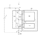
【解決手段】スイッチQ1とスイッチQ2とが所定の接続点11でカスコード接続され、スイッチQ1が接続点11と基準点12との間に設けられて構成されるカスコード素子10の制御回路100において、スイッチング制御部110は、スイッチQ1のスイッチング制御を行い、バイアス補助部120は、スイッチング制御部110によりスイッチング制御されたスイッチQ1のオフ期間中に、基準点11と接続点12との間の電圧である接続点電圧に対して補助的にバイアスする。そのため、スイッチング制御部110によりスイッチング制御されたスイッチQ1のオフ期間中に、スイッチQ2のゲート・ソース間電圧がスイッチQ2の閾値に対して十分負にバイアスされる。これにより、カスコード素子のスイッチング制御が安定化し、カスコード素子が破壊するのを防止することができる。
【選択図】図3
Description
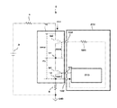
3:直流電源
4、5:抵抗
10:カスコード素子
11:接続点
12:基準点
100:制御回路
101、102、103、104:端子
110:スイッチング制御部
111:駆動部
112:発振部
113:駆動制御部
120:バイアス補助部
121:ダイオード
122:コンデンサ
123、125:抵抗
124:ツェナダイオード
Q1、Q2:スイッチ
Claims (10)
- ノーマリオフ型のローサイド半導体スイッチとノーマリオン型のハイサイド半導体スイッチとが所定の接続点でカスコード接続され、前記ローサイド半導体スイッチが前記接続点と前記カスコード素子の電気的な基準電位となる基準点との間に設けられて構成されるカスコード素子の制御回路において、
前記ローサイド半導体スイッチのスイッチング制御を行うスイッチング制御部と、
前記スイッチング制御部によりスイッチング制御された前記ローサイド半導体スイッチのオフ期間中に、前記基準点と前記接続点との間の電圧である接続点電圧に対して補助的にバイアスするバイアス補助部と、
を備えたことを特徴とする制御回路。 - 前記バイアス補助部は、ダイオード、コンデンサおよび抵抗を有し、前記ダイオードのアノード端子は前記接続点に接続され、前記ダイオードのカソード端子は前記コンデンサの一端に接続され、前記コンデンサの他端は前記基準点に接続され、前記抵抗は前記ダイオードに並列接続されていることを特徴とする請求項1に記載の制御回路。
- 前記バイアス補助部は、ツェナダイオードを有し、
前記ツェナダイオードのアノード端子は前記基準点に接続され、前記ツェナダイオードのカソード端子は前記接続点に接続されていることを特徴とする請求項2に記載の制御回路。 - 前記ハイサイド半導体スイッチは、高電子移動度トランジスタであることを特徴とする請求項1乃至3のいずれか1に記載の制御回路。
- 前記高電子移動度トランジスタは、窒化ガリウム、炭化ケイ素をチャネルに用いたものであることであることを特徴とする請求項4に記載の制御回路。
- 前記高電子移動度トランジスタは、酸化物半導体をチャネルに用いたものであることであることを特徴とする請求項4に記載の制御回路。
- 前記酸化物半導体は、酸化スズ、酸化亜鉛、酸化インジウム又はこれらを複合した複合酸化物半導体であることを特徴とする請求項6に記載の制御回路。
- 前記スイッチング制御部および前記バイアス補助部は、所定の半導体基板上にモノリシック集積回路として形成されることを特徴とする請求項1乃至7のいずれか1に記載の制御回路。
- 前記制御回路は、前記ローサイド半導体スイッチ及び/又は前記ハイサイド半導体スイッチと共に、モノリシック集積回路として形成されることを特徴とする請求項8に記載の制御回路。
- 前記制御回路は、前記ローサイド半導体スイッチ及び/又は前記ハイサイド半導体スイッチと共に、所定の樹脂モールドパッケージに搭載されることを特徴とする請求項1乃至9のいずれか1に記載の制御回路。
Priority Applications (1)
| Application Number | Priority Date | Filing Date | Title |
|---|---|---|---|
| JP2014139267A JP6265849B2 (ja) | 2014-07-07 | 2014-07-07 | 制御回路 |
Applications Claiming Priority (1)
| Application Number | Priority Date | Filing Date | Title |
|---|---|---|---|
| JP2014139267A JP6265849B2 (ja) | 2014-07-07 | 2014-07-07 | 制御回路 |
Publications (2)
| Publication Number | Publication Date |
|---|---|
| JP2016019314A true JP2016019314A (ja) | 2016-02-01 |
| JP6265849B2 JP6265849B2 (ja) | 2018-01-24 |
Family
ID=55234188
Family Applications (1)
| Application Number | Title | Priority Date | Filing Date |
|---|---|---|---|
| JP2014139267A Expired - Fee Related JP6265849B2 (ja) | 2014-07-07 | 2014-07-07 | 制御回路 |
Country Status (1)
| Country | Link |
|---|---|
| JP (1) | JP6265849B2 (ja) |
Citations (2)
| Publication number | Priority date | Publication date | Assignee | Title |
|---|---|---|---|---|
| JP2006324839A (ja) * | 2005-05-18 | 2006-11-30 | Fuji Electric Holdings Co Ltd | 複合型半導体装置 |
| WO2013146570A1 (ja) * | 2012-03-27 | 2013-10-03 | シャープ株式会社 | カスコード回路 |
-
2014
- 2014-07-07 JP JP2014139267A patent/JP6265849B2/ja not_active Expired - Fee Related
Patent Citations (2)
| Publication number | Priority date | Publication date | Assignee | Title |
|---|---|---|---|---|
| JP2006324839A (ja) * | 2005-05-18 | 2006-11-30 | Fuji Electric Holdings Co Ltd | 複合型半導体装置 |
| WO2013146570A1 (ja) * | 2012-03-27 | 2013-10-03 | シャープ株式会社 | カスコード回路 |
Also Published As
| Publication number | Publication date |
|---|---|
| JP6265849B2 (ja) | 2018-01-24 |
Similar Documents
| Publication | Publication Date | Title |
|---|---|---|
| JP4528321B2 (ja) | スイッチング回路、回路、並びにスイッチング回路及び駆動パルス生成回路を含む回路 | |
| JP6237038B2 (ja) | カスコードトランジスタ及びカスコードトランジスタの制御方法 | |
| US9362903B2 (en) | Gate drivers for circuits based on semiconductor devices | |
| CN104205638B (zh) | 共射共基电路 | |
| KR101329614B1 (ko) | 반도체장치 | |
| US9806706B2 (en) | Switching unit and power supply circuit | |
| JP2013070263A (ja) | 電力変換回路、多相ボルテージレギュレータ、及び電力変換方法 | |
| JP6065721B2 (ja) | 駆動回路、半導体集積回路、及び駆動回路の制御方法 | |
| JP6048929B2 (ja) | ゲート駆動回路、インバータ回路、電力変換装置および電気機器 | |
| JP6090007B2 (ja) | 駆動回路 | |
| JP6458552B2 (ja) | スイッチング方式の降圧型dc−dcコンバータ、及び電力変換回路 | |
| US9762232B2 (en) | Semiconductor device | |
| JP6572123B2 (ja) | ゲート駆動回路 | |
| JP6408146B2 (ja) | 複合型半導体装置 | |
| US10707870B2 (en) | High-side driver circuit | |
| JP6265849B2 (ja) | 制御回路 | |
| JP6256917B2 (ja) | カスコード素子 | |
| JP6278874B2 (ja) | 制御回路 | |
| JP5780489B2 (ja) | ゲート駆動回路 | |
| JP4830829B2 (ja) | 絶縁ゲートトランジスタの駆動回路 | |
| JP4821394B2 (ja) | 半導体素子駆動回路 | |
| JP6299869B2 (ja) | 絶縁ゲート型パワー半導体素子のゲート駆動回路 | |
| JP2016082335A (ja) | 半導体装置 | |
| CN117767238A (zh) | 浪涌电流抑制电路 | |
| JP2015138837A (ja) | 複合型半導体装置 |
Legal Events
| Date | Code | Title | Description |
|---|---|---|---|
| A621 | Written request for application examination |
Free format text: JAPANESE INTERMEDIATE CODE: A621 Effective date: 20161005 |
|
| A977 | Report on retrieval |
Free format text: JAPANESE INTERMEDIATE CODE: A971007 Effective date: 20170719 |
|
| A131 | Notification of reasons for refusal |
Free format text: JAPANESE INTERMEDIATE CODE: A131 Effective date: 20170808 |
|
| A521 | Request for written amendment filed |
Free format text: JAPANESE INTERMEDIATE CODE: A523 Effective date: 20170906 |
|
| A131 | Notification of reasons for refusal |
Free format text: JAPANESE INTERMEDIATE CODE: A131 Effective date: 20171003 |
|
| A521 | Request for written amendment filed |
Free format text: JAPANESE INTERMEDIATE CODE: A523 Effective date: 20171030 |
|
| TRDD | Decision of grant or rejection written | ||
| A01 | Written decision to grant a patent or to grant a registration (utility model) |
Free format text: JAPANESE INTERMEDIATE CODE: A01 Effective date: 20171219 |
|
| R150 | Certificate of patent or registration of utility model |
Ref document number: 6265849 Country of ref document: JP Free format text: JAPANESE INTERMEDIATE CODE: R150 |
|
| LAPS | Cancellation because of no payment of annual fees |