JP6065721B2 - 駆動回路、半導体集積回路、及び駆動回路の制御方法 - Google Patents
駆動回路、半導体集積回路、及び駆動回路の制御方法 Download PDFInfo
- Publication number
- JP6065721B2 JP6065721B2 JP2013080261A JP2013080261A JP6065721B2 JP 6065721 B2 JP6065721 B2 JP 6065721B2 JP 2013080261 A JP2013080261 A JP 2013080261A JP 2013080261 A JP2013080261 A JP 2013080261A JP 6065721 B2 JP6065721 B2 JP 6065721B2
- Authority
- JP
- Japan
- Prior art keywords
- switching element
- voltage
- transistor
- drive circuit
- turned
- Prior art date
- Legal status (The legal status is an assumption and is not a legal conclusion. Google has not performed a legal analysis and makes no representation as to the accuracy of the status listed.)
- Expired - Fee Related
Links
- 239000004065 semiconductor Substances 0.000 title claims description 23
- 238000000034 method Methods 0.000 title claims description 9
- 230000004044 response Effects 0.000 claims description 11
- 238000001514 detection method Methods 0.000 description 10
- 150000001875 compounds Chemical class 0.000 description 8
- 238000005516 engineering process Methods 0.000 description 7
- 239000000758 substrate Substances 0.000 description 7
- 230000007423 decrease Effects 0.000 description 6
- 238000010586 diagram Methods 0.000 description 6
- 239000003990 capacitor Substances 0.000 description 5
- 230000003071 parasitic effect Effects 0.000 description 5
- 230000002093 peripheral effect Effects 0.000 description 5
- JMASRVWKEDWRBT-UHFFFAOYSA-N Gallium nitride Chemical compound [Ga]#N JMASRVWKEDWRBT-UHFFFAOYSA-N 0.000 description 4
- HBMJWWWQQXIZIP-UHFFFAOYSA-N silicon carbide Chemical compound [Si+]#[C-] HBMJWWWQQXIZIP-UHFFFAOYSA-N 0.000 description 4
- XUIMIQQOPSSXEZ-UHFFFAOYSA-N Silicon Chemical compound [Si] XUIMIQQOPSSXEZ-UHFFFAOYSA-N 0.000 description 3
- 239000002131 composite material Substances 0.000 description 3
- 230000005669 field effect Effects 0.000 description 3
- 229910052710 silicon Inorganic materials 0.000 description 3
- 239000010703 silicon Substances 0.000 description 3
- 229910002601 GaN Inorganic materials 0.000 description 2
- 230000000295 complement effect Effects 0.000 description 2
- 229910010271 silicon carbide Inorganic materials 0.000 description 2
- 230000004888 barrier function Effects 0.000 description 1
- 230000000694 effects Effects 0.000 description 1
- 238000009499 grossing Methods 0.000 description 1
- 230000007246 mechanism Effects 0.000 description 1
- 229910044991 metal oxide Inorganic materials 0.000 description 1
- 150000004706 metal oxides Chemical class 0.000 description 1
- 230000008569 process Effects 0.000 description 1
- 230000001172 regenerating effect Effects 0.000 description 1
- 238000004804 winding Methods 0.000 description 1
Images




Classifications
-
- H—ELECTRICITY
- H03—ELECTRONIC CIRCUITRY
- H03K—PULSE TECHNIQUE
- H03K19/00—Logic circuits, i.e. having at least two inputs acting on one output; Inverting circuits
- H03K19/0008—Arrangements for reducing power consumption
- H03K19/0019—Arrangements for reducing power consumption by energy recovery or adiabatic operation
-
- H—ELECTRICITY
- H03—ELECTRONIC CIRCUITRY
- H03K—PULSE TECHNIQUE
- H03K17/00—Electronic switching or gating, i.e. not by contact-making and –breaking
- H03K17/08—Modifications for protecting switching circuit against overcurrent or overvoltage
- H03K17/081—Modifications for protecting switching circuit against overcurrent or overvoltage without feedback from the output circuit to the control circuit
- H03K17/0812—Modifications for protecting switching circuit against overcurrent or overvoltage without feedback from the output circuit to the control circuit by measures taken in the control circuit
- H03K17/08122—Modifications for protecting switching circuit against overcurrent or overvoltage without feedback from the output circuit to the control circuit by measures taken in the control circuit in field-effect transistor switches
-
- H—ELECTRICITY
- H03—ELECTRONIC CIRCUITRY
- H03K—PULSE TECHNIQUE
- H03K2217/00—Indexing scheme related to electronic switching or gating, i.e. not by contact-making or -breaking covered by H03K17/00
- H03K2217/0081—Power supply means, e.g. to the switch driver
Landscapes
- Physics & Mathematics (AREA)
- Engineering & Computer Science (AREA)
- Computer Hardware Design (AREA)
- Computing Systems (AREA)
- General Engineering & Computer Science (AREA)
- Mathematical Physics (AREA)
- Electronic Switches (AREA)
- Power Conversion In General (AREA)
Description
〔第1の実施形態〕
次に、開示の技術における第2の実施形態を説明する。第2の実施形態の基本的構成は、第1の実施形態と同様であり、第2の実施形態において第1の実施形態と同様の機能部品については、第1の実施形態と同様の符号を付与してその説明を省略する。
次に開示の技術に係る第3の実施形態を説明する。なお、第3の実施形態の基本的構成は、第1の実施形態と同様であり、第3の実施形態において第1の実施形態と同様の機能部品については、第1の実施形態と同様の符号を付与してその説明を省略する。
第1のスイッチング素子のソースに直列に接続され、前記第1のスイッチング素子がオンされるときにオンされ、前記第1のスイッチング素子がオフされるときにオフされる第2のスイッチング素子と、
前記第2のスイッチング素子のドレインと電源ラインとの間に設けられ、前記第2のスイッチング素子をオフさせる信号に応じて、前記第2のスイッチング素子のドレインを前記電源ラインに接続する通電素子と、
を含む駆動回路。
前記通電素子は第3のスイッチング素子を有し、
前記第1のスイッチング素子の駆動信号に応じ、前記第1のスイッチング素子、前記第2のスイッチング素子、及び前記第3のスイッチング素子のオン・オフの制御を行う制御部を含む付記1記載の駆動回路。
第1のスイッチング素子のソースに直列に接続された第2のスイッチング素子と、
前記第2のスイッチング素子のドレインと電源ラインとの間に接続された第3のスイッチング素子と、
前記第1のスイッチング素子の駆動信号に応じ、前記第1のスイッチング素子のゲートへ出力する電圧を制御し、前記第1のスイッチング素子をオンさせるときに、前記第2のスイッチング素子をオンさせ、かつ前記第3のスイッチング素子をオフさせ、前記第1のスイッチング素子をオフするときに、前記第2のスイッチング素子をオフさせ、かつ前記第3のスイッチング素子をオンさせる制御部と、
を含む駆動回路。
前記制御部は、前記第2のスイッチング素子をオフさせる前記制御信号に応じて前記第3のスイッチング素子をオンさせる、付記2又は付記3記載の駆動回路。
前記制御部は、前記第2のスイッチング素子をオフさせた後、前記第3のスイッチング素子をオンさせる、付記2又は付記3記載の駆動回路。
前記制御部は、前記第1のスイッチング素子のゲート電圧が所定値に低下することで前記第2のスイッチング素子をオフさせ、前記第3のスイッチング素子をオンさせる、付記4又は付記5記載の駆動回路。
前記第1のスイッチング素子が、ノーマリーオン形のスイッチング素子である、付記1から付記6のいずれかに記載の駆動回路。
第1のスイッチング素子のソースに直列に接続され、前記第1のスイッチング素子がオンされるときにオンされ、前記第1のスイッチング素子がオフされるときにオフされる第2のスイッチング素子と、
前記第2のスイッチング素子のドレインと電源ラインとの間に設けられ、前記第2のスイッチング素子をオフさせる制御信号に応じて、前記第2のスイッチング素子のドレインを前記電源ラインに接続する通電素子と、
を備える駆動回路を含む半導体集積回路
前記通電素子は第3のスイッチング素子を有し、
前記第1のスイッチング素子の駆動信号に応じ、第1のスイッチング素子、前記第2のスイッチング素子、及び前記第3のスイッチング素子のオン・オフの制御を行う制御部と、
を含む付記8記載の半導体集積回路。
第1のスイッチング素子のソースに直列に接続された第2のスイッチング素子と、
前記第2のスイッチング素子のドレインと電源ラインとの間に接続された第3のスイッチング素子と、
前記第1のスイッチング素子の駆動信号に応じ、第1のスイッチング素子のゲートへ出力する電圧を制御し、前記第1のスイッチング素子をオンさせるときに、前記第2のスイッチング素子をオンさせ、かつ前記第3のスイッチング素子をオフさせ、前記第1のスイッチング素子をオフするときに、前記第2のスイッチング素子をオフさせ、かつ前記第3のスイッチング素子をオンさせる制御部と、
を備える駆動回路を含む半導体集積回路。
前記制御部は、前記第2のスイッチング素子をオフさせる前記制御信号に応じて前記第3のスイッチング素子をオンさせる、付記9又は付記10記載の半導体集積回路。
前記制御部は、前記第2のスイッチング素子をオフさせた後、前記第3のスイッチング素子をオンさせる、付記9又は付記10記載の半導体集積回路。
前記制御部は、前記第1のスイッチング素子のゲート電圧が所定値に低下することで前記第2のスイッチング素子をオフさせ、前記第3のスイッチング素子をオンさせる、付記11又は付記12記載の半導体集積回路。
前記第1のスイッチング素子が、ノーマリーオン形のスイッチング素子である、付記8から付記13のいずれかに記載の半導体集積回路。
第1のスイッチング素子をオンする際に、前記第1のスイッチング素子のソースに直列に接続された第2のスイッチング素子をオンし、
前記第1のスイッチング素子をオフする際に、前記第2のスイッチング素子をオフし、 前記第2のスイッチング素子のドレインと電源ラインとの間に設けた通電素子により前記第2のスイッチング素子のドレインを前記電源ラインに接続する、
ことを含む駆動回路の制御方法。
前記通電素子は第3のスイッチング素子を有し、前記第3のスイッチング素子をオンすることで、前記第2のスイッチング素子のドレインを前記電源ラインに接続する、
ことを含む付記15記載の駆動回路の制御方法。
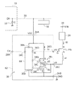
12、52、62、72 集積回路
14 基板
16 直流電源部
18 周辺回路
20 電源ライン
22 コンデンサ
28 負荷
30 電源ライン
32 パッケージ
34 リード
36、74 コントロール回路
40 ノード
42 ゲート電圧制御部
44 ゲート電圧検出部
46、68 制御信号出力部
66 ソース電圧検出部
74 ダイオード
PTr パワートランジスタ
PTs パワートランジスタ
Ma トランジスタ
Mb トランジスタ
Claims (5)
- 第1のスイッチング素子のソースに直列に接続され、前記第1のスイッチング素子がオンされるときにオンされ、前記第1のスイッチング素子がオフされるときにオフされる第2のスイッチング素子と、
前記第2のスイッチング素子のドレインと電源ラインとの間に設けられ、前記第2のスイッチング素子をオフさせる信号に応じて、前記第2のスイッチング素子のドレインを前記電源ラインに接続する第3のスイッチング素子と、
前記第1のスイッチング素子の駆動信号に応じ、前記第1のスイッチング素子、前記第2のスイッチング素子、及び前記第3のスイッチング素子のオン・オフの制御を行う制御部と、
を含む駆動回路。 - 前記制御部は、前記第2のスイッチング素子をオフさせる前記駆動信号に応じて前記第3のスイッチング素子をオンさせる、請求項1記載の駆動回路。
- 第1のスイッチング素子のソースに直列に接続され、前記第1のスイッチング素子がオンされるときにオンされ、前記第1のスイッチング素子がオフされるときにオフされる第2のスイッチング素子と、
前記第2のスイッチング素子のドレインと電源ラインとの間に設けられ、前記第2のスイッチング素子をオフさせる制御信号に応じて、前記第2のスイッチング素子のドレインを前記電源ラインに接続する第3のスイッチング素子と、
前記第1のスイッチング素子の駆動信号に応じ、第1のスイッチング素子、前記第2のスイッチング素子、及び前記第3のスイッチング素子のオン・オフ制御を行う制御部と、
を備えた駆動回路を含む半導体集積回路。 - 前記制御部は、前記第2のスイッチング素子をオフさせる前記駆動信号に応じて前記第3のスイッチング素子をオンさせる、請求項3記載の半導体集積回路。
- 制御部が、第1のスイッチング素子をオンする際に、前記第1のスイッチング素子のソースに直列に接続された第2のスイッチング素子をオンし、前記第2のスイッチング素子のドレインと電源ラインとの間に設けた第3のスイッチング素子をオフし、
前記制御部が、前記第1のスイッチング素子をオフする際に、前記第2のスイッチング素子をオフし、前記第3のスイッチング素子をオンすることにより前記第2のスイッチング素子のドレインを前記電源ラインに接続し、
前記制御部は、前記第1のスイッチング素子の駆動信号に応じ、前記第1のスイッチング素子、前記第2のスイッチング素子、及び前記第3のスイッチング素子のオン・オフの制御を行う、
ことを含む駆動回路の制御方法。
Priority Applications (3)
| Application Number | Priority Date | Filing Date | Title |
|---|---|---|---|
| JP2013080261A JP6065721B2 (ja) | 2013-04-08 | 2013-04-08 | 駆動回路、半導体集積回路、及び駆動回路の制御方法 |
| US14/229,332 US9059697B2 (en) | 2013-04-08 | 2014-03-28 | Drive circuit and drive method for driving normally-on-type transistor |
| CN201410126132.9A CN104104369B (zh) | 2013-04-08 | 2014-03-31 | 驱动电路、半导体集成电路和驱动电路的控制方法 |
Applications Claiming Priority (1)
| Application Number | Priority Date | Filing Date | Title |
|---|---|---|---|
| JP2013080261A JP6065721B2 (ja) | 2013-04-08 | 2013-04-08 | 駆動回路、半導体集積回路、及び駆動回路の制御方法 |
Publications (2)
| Publication Number | Publication Date |
|---|---|
| JP2014204354A JP2014204354A (ja) | 2014-10-27 |
| JP6065721B2 true JP6065721B2 (ja) | 2017-01-25 |
Family
ID=51654014
Family Applications (1)
| Application Number | Title | Priority Date | Filing Date |
|---|---|---|---|
| JP2013080261A Expired - Fee Related JP6065721B2 (ja) | 2013-04-08 | 2013-04-08 | 駆動回路、半導体集積回路、及び駆動回路の制御方法 |
Country Status (3)
| Country | Link |
|---|---|
| US (1) | US9059697B2 (ja) |
| JP (1) | JP6065721B2 (ja) |
| CN (1) | CN104104369B (ja) |
Families Citing this family (8)
| Publication number | Priority date | Publication date | Assignee | Title |
|---|---|---|---|---|
| JP2016139997A (ja) * | 2015-01-28 | 2016-08-04 | 株式会社東芝 | 半導体装置 |
| JP2016139996A (ja) * | 2015-01-28 | 2016-08-04 | 株式会社東芝 | 半導体装置 |
| CN107852157B (zh) * | 2015-05-27 | 2021-11-02 | 威电科技有限公司 | 开关电源装置 |
| US9813009B1 (en) * | 2017-02-07 | 2017-11-07 | Ford Global Technologies, Llc | Active gate clamping for inverter switching devices using grounded gate terminals |
| TWI705664B (zh) * | 2020-01-08 | 2020-09-21 | 大陸商上海瀚薪科技有限公司 | 一種碳化矽功率元件、驅動電路及控制方法 |
| CN113162377B (zh) * | 2020-01-22 | 2025-03-21 | 上海瀚薪科技有限公司 | 一种碳化硅功率组件、驱动电路及控制方法 |
| JP7610402B2 (ja) * | 2020-12-22 | 2025-01-08 | 日立Astemo株式会社 | 負荷駆動装置 |
| US20240283351A1 (en) * | 2023-02-17 | 2024-08-22 | Power Integrations, Inc. | Detecting signals from cascode power devices |
Family Cites Families (10)
| Publication number | Priority date | Publication date | Assignee | Title |
|---|---|---|---|---|
| JPH10276076A (ja) | 1997-03-31 | 1998-10-13 | Oki Electric Ind Co Ltd | 半導体回路 |
| US6097220A (en) * | 1997-06-11 | 2000-08-01 | Intel Corporation | Method and circuit for recycling charge |
| WO2005031956A1 (en) * | 2003-09-25 | 2005-04-07 | Koninklijke Philips Electronics N.V. | A switch mode power converter |
| US7928702B2 (en) * | 2005-04-13 | 2011-04-19 | International Rectifier Corporation | Driving circuit for use with high voltage depletion-mode semiconductor switches |
| JP4844007B2 (ja) | 2005-05-18 | 2011-12-21 | 富士電機株式会社 | 複合型半導体装置 |
| US8330492B2 (en) * | 2006-06-02 | 2012-12-11 | Semiconductor Energy Laboratory Co., Ltd. | Liquid crystal display device and electronic device |
| US7567097B2 (en) * | 2007-09-29 | 2009-07-28 | Hewlett-Packard Development Company, L.P. | Pre-driver circuit and appparatus using same |
| JP5565336B2 (ja) * | 2011-02-14 | 2014-08-06 | 富士通セミコンダクター株式会社 | 出力回路、システム、及び出力回路の制御方法 |
| JP5910395B2 (ja) * | 2011-09-16 | 2016-04-27 | サンケン電気株式会社 | ドライブ回路 |
| WO2013146570A1 (ja) * | 2012-03-27 | 2013-10-03 | シャープ株式会社 | カスコード回路 |
-
2013
- 2013-04-08 JP JP2013080261A patent/JP6065721B2/ja not_active Expired - Fee Related
-
2014
- 2014-03-28 US US14/229,332 patent/US9059697B2/en not_active Expired - Fee Related
- 2014-03-31 CN CN201410126132.9A patent/CN104104369B/zh not_active Expired - Fee Related
Also Published As
| Publication number | Publication date |
|---|---|
| CN104104369A (zh) | 2014-10-15 |
| JP2014204354A (ja) | 2014-10-27 |
| CN104104369B (zh) | 2017-09-01 |
| US20140300394A1 (en) | 2014-10-09 |
| US9059697B2 (en) | 2015-06-16 |
Similar Documents
| Publication | Publication Date | Title |
|---|---|---|
| JP2014204354A (ja) | 駆動回路、半導体集積回路、及び駆動回路の制御方法 | |
| US9935551B2 (en) | Switching circuit including serially connected transistors for reducing transient current at time of turning off, and power supply circuit provided therewith | |
| JP6402591B2 (ja) | 半導体装置 | |
| US8648643B2 (en) | Semiconductor power modules and devices | |
| US9059076B2 (en) | Gate drivers for circuits based on semiconductor devices | |
| JP6264491B1 (ja) | 短絡検出装置および装置 | |
| JP5263317B2 (ja) | 半導体スイッチング素子の駆動回路 | |
| JP2020018164A (ja) | 回路を動作させる方法及び回路 | |
| CN112019200A (zh) | 包括故障安全下拉电路的功率器件和电子开关器件 | |
| CN104205638B (zh) | 共射共基电路 | |
| CN106688183A (zh) | 自灭弧式半导体元件的短路保护电路 | |
| WO2013077105A1 (ja) | インバータ装置 | |
| KR102112299B1 (ko) | 파워 스위치 소자의 구동 방법 및 구동 회로 | |
| JP5619673B2 (ja) | スイッチング回路及び半導体モジュール | |
| CN111758210B (zh) | 整流电路以及电源装置 | |
| JP6988256B2 (ja) | 電力変換器 | |
| CN112534668B (zh) | 升压转换器短路保护 | |
| KR20250148461A (ko) | 온-저항을 감소시키고 단락 내성 시간을 연장시키도록 동작 가능한 전력 스위칭 디바이스 | |
| KR20190011494A (ko) | SiC MOSFET용 게이트 구동회로 | |
| US9991776B2 (en) | Switched mode power supply converter | |
| JP5843535B2 (ja) | 半導体モジュール | |
| WO2016030998A1 (ja) | 電力変換装置、モータ装置および逆変換器モジュール | |
| JP5862232B2 (ja) | 過電圧保護回路 | |
| JP6950443B2 (ja) | 半導体スイッチング素子駆動回路及び電力変換器 | |
| CN110741546B (zh) | 整流电路以及电源装置 |
Legal Events
| Date | Code | Title | Description |
|---|---|---|---|
| A711 | Notification of change in applicant |
Free format text: JAPANESE INTERMEDIATE CODE: A712 Effective date: 20150608 |
|
| A621 | Written request for application examination |
Free format text: JAPANESE INTERMEDIATE CODE: A621 Effective date: 20160105 |
|
| A977 | Report on retrieval |
Free format text: JAPANESE INTERMEDIATE CODE: A971007 Effective date: 20160804 |
|
| A131 | Notification of reasons for refusal |
Free format text: JAPANESE INTERMEDIATE CODE: A131 Effective date: 20160809 |
|
| A521 | Request for written amendment filed |
Free format text: JAPANESE INTERMEDIATE CODE: A523 Effective date: 20161005 |
|
| TRDD | Decision of grant or rejection written | ||
| A01 | Written decision to grant a patent or to grant a registration (utility model) |
Free format text: JAPANESE INTERMEDIATE CODE: A01 Effective date: 20161129 |
|
| A61 | First payment of annual fees (during grant procedure) |
Free format text: JAPANESE INTERMEDIATE CODE: A61 Effective date: 20161212 |
|
| R150 | Certificate of patent or registration of utility model |
Ref document number: 6065721 Country of ref document: JP Free format text: JAPANESE INTERMEDIATE CODE: R150 |
|
| LAPS | Cancellation because of no payment of annual fees |