JP2016100466A - 半導体装置及び半導体装置の製造方法 - Google Patents
半導体装置及び半導体装置の製造方法 Download PDFInfo
- Publication number
- JP2016100466A JP2016100466A JP2014236545A JP2014236545A JP2016100466A JP 2016100466 A JP2016100466 A JP 2016100466A JP 2014236545 A JP2014236545 A JP 2014236545A JP 2014236545 A JP2014236545 A JP 2014236545A JP 2016100466 A JP2016100466 A JP 2016100466A
- Authority
- JP
- Japan
- Prior art keywords
- region
- trench
- conductivity type
- insulating layer
- semiconductor substrate
- Prior art date
- Legal status (The legal status is an assumption and is not a legal conclusion. Google has not performed a legal analysis and makes no representation as to the accuracy of the status listed.)
- Pending
Links
Images


Classifications
-
- H—ELECTRICITY
- H10—SEMICONDUCTOR DEVICES; ELECTRIC SOLID-STATE DEVICES NOT OTHERWISE PROVIDED FOR
- H10D—INORGANIC ELECTRIC SEMICONDUCTOR DEVICES
- H10D30/00—Field-effect transistors [FET]
- H10D30/60—Insulated-gate field-effect transistors [IGFET]
- H10D30/64—Double-diffused metal-oxide semiconductor [DMOS] FETs
- H10D30/66—Vertical DMOS [VDMOS] FETs
- H10D30/668—Vertical DMOS [VDMOS] FETs having trench gate electrodes, e.g. UMOS transistors
-
- H—ELECTRICITY
- H10—SEMICONDUCTOR DEVICES; ELECTRIC SOLID-STATE DEVICES NOT OTHERWISE PROVIDED FOR
- H10D—INORGANIC ELECTRIC SEMICONDUCTOR DEVICES
- H10D30/00—Field-effect transistors [FET]
- H10D30/60—Insulated-gate field-effect transistors [IGFET]
- H10D30/601—Insulated-gate field-effect transistors [IGFET] having lightly-doped drain or source extensions, e.g. LDD IGFETs or DDD IGFETs
- H10D30/608—Insulated-gate field-effect transistors [IGFET] having lightly-doped drain or source extensions, e.g. LDD IGFETs or DDD IGFETs having non-planar bodies, e.g. having recessed gate electrodes
-
- H—ELECTRICITY
- H10—SEMICONDUCTOR DEVICES; ELECTRIC SOLID-STATE DEVICES NOT OTHERWISE PROVIDED FOR
- H10D—INORGANIC ELECTRIC SEMICONDUCTOR DEVICES
- H10D30/00—Field-effect transistors [FET]
- H10D30/01—Manufacture or treatment
- H10D30/021—Manufacture or treatment of FETs having insulated gates [IGFET]
- H10D30/022—Manufacture or treatment of FETs having insulated gates [IGFET] having lightly-doped source or drain extensions selectively formed at the sides of the gates
-
- H—ELECTRICITY
- H10—SEMICONDUCTOR DEVICES; ELECTRIC SOLID-STATE DEVICES NOT OTHERWISE PROVIDED FOR
- H10D—INORGANIC ELECTRIC SEMICONDUCTOR DEVICES
- H10D30/00—Field-effect transistors [FET]
- H10D30/01—Manufacture or treatment
- H10D30/021—Manufacture or treatment of FETs having insulated gates [IGFET]
- H10D30/028—Manufacture or treatment of FETs having insulated gates [IGFET] of double-diffused metal oxide semiconductor [DMOS] FETs
- H10D30/0291—Manufacture or treatment of FETs having insulated gates [IGFET] of double-diffused metal oxide semiconductor [DMOS] FETs of vertical DMOS [VDMOS] FETs
- H10D30/0297—Manufacture or treatment of FETs having insulated gates [IGFET] of double-diffused metal oxide semiconductor [DMOS] FETs of vertical DMOS [VDMOS] FETs using recessing of the gate electrodes, e.g. to form trench gate electrodes
-
- H—ELECTRICITY
- H10—SEMICONDUCTOR DEVICES; ELECTRIC SOLID-STATE DEVICES NOT OTHERWISE PROVIDED FOR
- H10D—INORGANIC ELECTRIC SEMICONDUCTOR DEVICES
- H10D62/00—Semiconductor bodies, or regions thereof, of devices having potential barriers
- H10D62/10—Shapes, relative sizes or dispositions of the regions of the semiconductor bodies; Shapes of the semiconductor bodies
- H10D62/102—Constructional design considerations for preventing surface leakage or controlling electric field concentration
- H10D62/103—Constructional design considerations for preventing surface leakage or controlling electric field concentration for increasing or controlling the breakdown voltage of reverse-biased devices
- H10D62/105—Constructional design considerations for preventing surface leakage or controlling electric field concentration for increasing or controlling the breakdown voltage of reverse-biased devices by having particular doping profiles, shapes or arrangements of PN junctions; by having supplementary regions, e.g. junction termination extension [JTE]
- H10D62/106—Constructional design considerations for preventing surface leakage or controlling electric field concentration for increasing or controlling the breakdown voltage of reverse-biased devices by having particular doping profiles, shapes or arrangements of PN junctions; by having supplementary regions, e.g. junction termination extension [JTE] having supplementary regions doped oppositely to or in rectifying contact with regions of the semiconductor bodies, e.g. guard rings with PN or Schottky junctions
- H10D62/107—Buried supplementary regions, e.g. buried guard rings
-
- H—ELECTRICITY
- H10—SEMICONDUCTOR DEVICES; ELECTRIC SOLID-STATE DEVICES NOT OTHERWISE PROVIDED FOR
- H10D—INORGANIC ELECTRIC SEMICONDUCTOR DEVICES
- H10D62/00—Semiconductor bodies, or regions thereof, of devices having potential barriers
- H10D62/10—Shapes, relative sizes or dispositions of the regions of the semiconductor bodies; Shapes of the semiconductor bodies
- H10D62/13—Semiconductor regions connected to electrodes carrying current to be rectified, amplified or switched, e.g. source or drain regions
- H10D62/149—Source or drain regions of field-effect devices
- H10D62/151—Source or drain regions of field-effect devices of IGFETs
- H10D62/156—Drain regions of DMOS transistors
- H10D62/157—Impurity concentrations or distributions
-
- H—ELECTRICITY
- H10—SEMICONDUCTOR DEVICES; ELECTRIC SOLID-STATE DEVICES NOT OTHERWISE PROVIDED FOR
- H10D—INORGANIC ELECTRIC SEMICONDUCTOR DEVICES
- H10D62/00—Semiconductor bodies, or regions thereof, of devices having potential barriers
- H10D62/10—Shapes, relative sizes or dispositions of the regions of the semiconductor bodies; Shapes of the semiconductor bodies
- H10D62/17—Semiconductor regions connected to electrodes not carrying current to be rectified, amplified or switched, e.g. channel regions
- H10D62/213—Channel regions of field-effect devices
- H10D62/221—Channel regions of field-effect devices of FETs
- H10D62/235—Channel regions of field-effect devices of FETs of IGFETs
-
- H—ELECTRICITY
- H10—SEMICONDUCTOR DEVICES; ELECTRIC SOLID-STATE DEVICES NOT OTHERWISE PROVIDED FOR
- H10D—INORGANIC ELECTRIC SEMICONDUCTOR DEVICES
- H10D62/00—Semiconductor bodies, or regions thereof, of devices having potential barriers
- H10D62/10—Shapes, relative sizes or dispositions of the regions of the semiconductor bodies; Shapes of the semiconductor bodies
- H10D62/17—Semiconductor regions connected to electrodes not carrying current to be rectified, amplified or switched, e.g. channel regions
- H10D62/393—Body regions of DMOS transistors or IGBTs
-
- H—ELECTRICITY
- H10—SEMICONDUCTOR DEVICES; ELECTRIC SOLID-STATE DEVICES NOT OTHERWISE PROVIDED FOR
- H10D—INORGANIC ELECTRIC SEMICONDUCTOR DEVICES
- H10D64/00—Electrodes of devices having potential barriers
- H10D64/20—Electrodes characterised by their shapes, relative sizes or dispositions
- H10D64/27—Electrodes not carrying the current to be rectified, amplified, oscillated or switched, e.g. gates
- H10D64/311—Gate electrodes for field-effect devices
- H10D64/411—Gate electrodes for field-effect devices for FETs
- H10D64/511—Gate electrodes for field-effect devices for FETs for IGFETs
- H10D64/514—Gate electrodes for field-effect devices for FETs for IGFETs characterised by the insulating layers
- H10D64/516—Gate electrodes for field-effect devices for FETs for IGFETs characterised by the insulating layers the thicknesses being non-uniform
-
- H—ELECTRICITY
- H10—SEMICONDUCTOR DEVICES; ELECTRIC SOLID-STATE DEVICES NOT OTHERWISE PROVIDED FOR
- H10D—INORGANIC ELECTRIC SEMICONDUCTOR DEVICES
- H10D64/00—Electrodes of devices having potential barriers
- H10D64/20—Electrodes characterised by their shapes, relative sizes or dispositions
- H10D64/27—Electrodes not carrying the current to be rectified, amplified, oscillated or switched, e.g. gates
- H10D64/311—Gate electrodes for field-effect devices
- H10D64/411—Gate electrodes for field-effect devices for FETs
- H10D64/511—Gate electrodes for field-effect devices for FETs for IGFETs
- H10D64/517—Gate electrodes for field-effect devices for FETs for IGFETs characterised by the conducting layers
- H10D64/518—Gate electrodes for field-effect devices for FETs for IGFETs characterised by the conducting layers characterised by their lengths or sectional shapes
-
- H—ELECTRICITY
- H10—SEMICONDUCTOR DEVICES; ELECTRIC SOLID-STATE DEVICES NOT OTHERWISE PROVIDED FOR
- H10P—GENERIC PROCESSES OR APPARATUS FOR THE MANUFACTURE OR TREATMENT OF DEVICES COVERED BY CLASS H10
- H10P50/00—Etching of wafers, substrates or parts of devices
- H10P50/20—Dry etching; Plasma etching; Reactive-ion etching
- H10P50/24—Dry etching; Plasma etching; Reactive-ion etching of semiconductor materials
- H10P50/242—Dry etching; Plasma etching; Reactive-ion etching of semiconductor materials of Group IV materials
-
- H—ELECTRICITY
- H10—SEMICONDUCTOR DEVICES; ELECTRIC SOLID-STATE DEVICES NOT OTHERWISE PROVIDED FOR
- H10P—GENERIC PROCESSES OR APPARATUS FOR THE MANUFACTURE OR TREATMENT OF DEVICES COVERED BY CLASS H10
- H10P50/00—Etching of wafers, substrates or parts of devices
- H10P50/69—Etching of wafers, substrates or parts of devices using masks for semiconductor materials
- H10P50/691—Etching of wafers, substrates or parts of devices using masks for semiconductor materials for Group V materials or Group III-V materials
- H10P50/693—Etching of wafers, substrates or parts of devices using masks for semiconductor materials for Group V materials or Group III-V materials characterised by their size, orientation, disposition, behaviour or shape, in horizontal or vertical plane
Landscapes
- Electrodes Of Semiconductors (AREA)
- Chemical & Material Sciences (AREA)
- Chemical Kinetics & Catalysis (AREA)
- General Chemical & Material Sciences (AREA)
- Insulated Gate Type Field-Effect Transistor (AREA)
Abstract
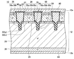
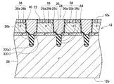
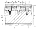
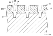
【解決手段】 半導体装置であって、表面にトレンチが形成されている半導体基板と、トレンチ内のゲート絶縁層及びゲート電極を有している。トレンチの側面に、段差が形成されている。トレンチの側面が、上部側面と、段差の表面と、下部側面を有している。半導体基板が、上部側面においてゲート絶縁層に接している第1導電型の第1領域と、第1領域に接する位置から段差よりも下側の位置に跨って配置されており、第1領域の下側の上部側面においてゲート絶縁層に接している第2導電型のボディ領域と、ボディ領域の下側に配置されており、下部側面においてゲート絶縁層に接している第1導電型の第2領域と、段差の表面においてゲート絶縁層に接しており、第2領域と繋がっている第1導電型の側部領域を有している。
【選択図】図1
Description
本明細書または図面に説明した技術要素は、単独あるいは各種の組み合わせによって技術有用性を発揮するものであり、出願時請求項記載の組み合わせに限定されるものではない。また、本明細書または図面に例示した技術は複数目的を同時に達成するものであり、そのうちの1つの目的を達成すること自体で技術有用性を持つものである。
12:半導体基板
22:ソース領域
26:ボディ領域
26a:高濃度領域
26b:上部領域
26c:下部領域
28:ドリフト領域
30:ドレイン領域
32:底部領域
33:側部領域
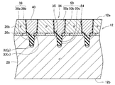
34:トレンチ
35:段差
36:層間絶縁層
38:ゲート絶縁層
38a:底部絶縁層
38b:側部絶縁膜
40:ゲート電極
Claims (7)
- 半導体装置であって、
表面にトレンチが形成されている半導体基板と、
前記トレンチの内面を覆っているゲート絶縁層と、
前記トレンチ内に配置されているゲート電極、
を有しており、
前記トレンチの側面に、段差が形成されており、
前記トレンチの前記側面が、前記段差よりも上側に位置する上部側面と、前記段差の表面と、前記段差よりも下側に位置する下部側面を有しており、
前記半導体基板が、
前記上部側面において前記ゲート絶縁層に接している第1導電型の第1領域と、
前記第1領域に接する位置から前記段差よりも下側の位置に跨って配置されており、前記第1領域の下側の前記上部側面において前記ゲート絶縁層に接している第2導電型のボディ領域と、
前記ボディ領域の下側に配置されており、前記下部側面において前記ゲート絶縁層に接している第1導電型の第2領域と、
前記段差の表面において前記ゲート絶縁層に接しており、前記第2領域と繋がっている第1導電型の側部領域、
を有している半導体装置。 - 前記段差の表面が、前記トレンチの中心側に向かうほど下側に変位するように傾斜している請求項1の半導体装置。
- 前記ボディ領域が、上部領域と、前記上部領域よりも第2導電型不純物濃度が低いとともに前記上部領域の下側に配置されている下部領域を有しており、
前記段差が、前記上部領域と前記下部領域の境界の位置または前記境界よりも下側に形成されている、
請求項1または2の半導体装置。 - 半導体装置を製造する方法であって、
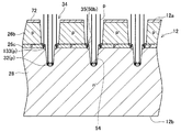
第1導電型の第2領域と、前記第2領域上に配置されている第1導電型のボディ領域を有する半導体基板に、前記ボディ領域を貫通して前記第2領域に達するとともに前記第2領域よりも上側の側面に段差を有するトレンチを形成する工程と、
前記段差の表面に第1導電型不純物を注入することによって、前記段差の表面に露出しており、前記第2領域と繋がっている第1導電型の側部領域を形成する工程と、
前記トレンチの内面を覆うゲート絶縁層を形成する工程と、
前記トレンチ内にゲート電極を形成する工程と、
前記半導体基板中に、第1導電型の第1領域を形成する工程、
を有し、
前記半導体装置において、前記第1領域が、前記段差よりも上側に位置する前記トレンチの前記側面において前記ゲート絶縁層に接している、
方法。 - 前記ボディ領域が、前記第2領域上に配置されている下部領域と、前記下部領域上に配置されているとともに前記下部領域よりも第2導電型不純物濃度が高い上部領域を有しており、
前記トレンチを形成する工程において、前記半導体基板をエッチングすることによって、前記上部領域と前記下部領域を貫通して前記第2領域に達するトレンチを形成する、
請求項4の方法。 - 前記方法が、
前記トレンチの底面に第2導電型不純物を注入することによって、前記底面に露出する第2導電型の底部領域を形成する工程をさらに有し、
前記ゲート絶縁層を形成する工程が、
前記第2導電型不純物の前記注入後であって、前記第1導電型不純物の前記注入前に、前記段差よりも下側の前記トレンチ内に底部絶縁層を形成する工程と、
前記第1導電型不純物の前記注入後に、前記底部絶縁層よりも上側の前記トレンチの前記側面に側部絶縁膜を形成する工程、
を有する請求項4または5の方法。 - 前記段差の表面に第1導電型不純物を注入する工程において、前記トレンチに隣接する前記半導体基板の表面に対して第1導電型不純物を注入する請求項4〜6の方法。
Priority Applications (4)
| Application Number | Priority Date | Filing Date | Title |
|---|---|---|---|
| JP2014236545A JP2016100466A (ja) | 2014-11-21 | 2014-11-21 | 半導体装置及び半導体装置の製造方法 |
| US14/939,720 US20160149029A1 (en) | 2014-11-21 | 2015-11-12 | Semiconductor device and method for manufacturing semiconductor device |
| CN201510811532.8A CN105633162A (zh) | 2014-11-21 | 2015-11-20 | 半导体装置以及半导体装置的制造方法 |
| DE102015120148.8A DE102015120148A1 (de) | 2014-11-21 | 2015-11-20 | Halbleiterbauelement und Verfahren zur Herstellung von Halbleiterbauelement |
Applications Claiming Priority (1)
| Application Number | Priority Date | Filing Date | Title |
|---|---|---|---|
| JP2014236545A JP2016100466A (ja) | 2014-11-21 | 2014-11-21 | 半導体装置及び半導体装置の製造方法 |
Publications (1)
| Publication Number | Publication Date |
|---|---|
| JP2016100466A true JP2016100466A (ja) | 2016-05-30 |
Family
ID=55914339
Family Applications (1)
| Application Number | Title | Priority Date | Filing Date |
|---|---|---|---|
| JP2014236545A Pending JP2016100466A (ja) | 2014-11-21 | 2014-11-21 | 半導体装置及び半導体装置の製造方法 |
Country Status (4)
| Country | Link |
|---|---|
| US (1) | US20160149029A1 (ja) |
| JP (1) | JP2016100466A (ja) |
| CN (1) | CN105633162A (ja) |
| DE (1) | DE102015120148A1 (ja) |
Cited By (4)
| Publication number | Priority date | Publication date | Assignee | Title |
|---|---|---|---|---|
| JP2018074013A (ja) * | 2016-10-31 | 2018-05-10 | 株式会社東芝 | 半導体装置及びその製造方法 |
| JP2020113796A (ja) * | 2016-10-31 | 2020-07-27 | 株式会社東芝 | 半導体装置及びその製造方法 |
| US11276751B2 (en) | 2019-08-07 | 2022-03-15 | Kabushiki Kaisha Toshiba | Semiconductor device, inverter circuit, driving device, vehicle, and elevator |
| US11355592B2 (en) | 2020-03-19 | 2022-06-07 | Kabushiki Kaisha Toshiba | Semiconductor device, method of manufacturing semiconductor device, inverter circuit, drive device, vehicle, and elevator |
Families Citing this family (6)
| Publication number | Priority date | Publication date | Assignee | Title |
|---|---|---|---|---|
| JP6560141B2 (ja) * | 2016-02-26 | 2019-08-14 | トヨタ自動車株式会社 | スイッチング素子 |
| JP6560142B2 (ja) * | 2016-02-26 | 2019-08-14 | トヨタ自動車株式会社 | スイッチング素子 |
| EP4122897A1 (en) * | 2017-01-05 | 2023-01-25 | Magic Leap, Inc. | Patterning of high refractive index glasses by plasma etching |
| CN113990801B (zh) * | 2021-11-17 | 2025-01-28 | 湖北九峰山实验室 | 多级沟槽半导体器件及其制作方法 |
| JP7717010B2 (ja) * | 2022-03-08 | 2025-08-01 | 株式会社デンソー | 半導体装置 |
| CN114783880A (zh) * | 2022-04-02 | 2022-07-22 | 致瞻科技(上海)有限公司 | 一种碳化硅mosfet器件及其制造方法 |
Citations (3)
| Publication number | Priority date | Publication date | Assignee | Title |
|---|---|---|---|---|
| JPH08167711A (ja) * | 1994-12-13 | 1996-06-25 | Mitsubishi Electric Corp | 絶縁ゲート型半導体装置およびその製造方法 |
| JP2008546216A (ja) * | 2005-06-10 | 2008-12-18 | フェアチャイルド・セミコンダクター・コーポレーション | 電荷平衡電界効果トランジスタ |
| JP2009054638A (ja) * | 2007-08-23 | 2009-03-12 | Toyota Motor Corp | 半導体装置とその製造方法 |
Family Cites Families (3)
| Publication number | Priority date | Publication date | Assignee | Title |
|---|---|---|---|---|
| JP4414863B2 (ja) | 2004-10-29 | 2010-02-10 | トヨタ自動車株式会社 | 絶縁ゲート型半導体装置およびその製造方法 |
| JP2009170629A (ja) * | 2008-01-16 | 2009-07-30 | Nec Electronics Corp | 半導体装置の製造方法 |
| JP5849882B2 (ja) * | 2011-09-27 | 2016-02-03 | 株式会社デンソー | 縦型半導体素子を備えた半導体装置 |
-
2014
- 2014-11-21 JP JP2014236545A patent/JP2016100466A/ja active Pending
-
2015
- 2015-11-12 US US14/939,720 patent/US20160149029A1/en not_active Abandoned
- 2015-11-20 CN CN201510811532.8A patent/CN105633162A/zh active Pending
- 2015-11-20 DE DE102015120148.8A patent/DE102015120148A1/de not_active Withdrawn
Patent Citations (3)
| Publication number | Priority date | Publication date | Assignee | Title |
|---|---|---|---|---|
| JPH08167711A (ja) * | 1994-12-13 | 1996-06-25 | Mitsubishi Electric Corp | 絶縁ゲート型半導体装置およびその製造方法 |
| JP2008546216A (ja) * | 2005-06-10 | 2008-12-18 | フェアチャイルド・セミコンダクター・コーポレーション | 電荷平衡電界効果トランジスタ |
| JP2009054638A (ja) * | 2007-08-23 | 2009-03-12 | Toyota Motor Corp | 半導体装置とその製造方法 |
Cited By (5)
| Publication number | Priority date | Publication date | Assignee | Title |
|---|---|---|---|---|
| JP2018074013A (ja) * | 2016-10-31 | 2018-05-10 | 株式会社東芝 | 半導体装置及びその製造方法 |
| US10600863B2 (en) | 2016-10-31 | 2020-03-24 | Kabushiki Kaisha Toshiba | Semiconductor device and method for manufacturing the same |
| JP2020113796A (ja) * | 2016-10-31 | 2020-07-27 | 株式会社東芝 | 半導体装置及びその製造方法 |
| US11276751B2 (en) | 2019-08-07 | 2022-03-15 | Kabushiki Kaisha Toshiba | Semiconductor device, inverter circuit, driving device, vehicle, and elevator |
| US11355592B2 (en) | 2020-03-19 | 2022-06-07 | Kabushiki Kaisha Toshiba | Semiconductor device, method of manufacturing semiconductor device, inverter circuit, drive device, vehicle, and elevator |
Also Published As
| Publication number | Publication date |
|---|---|
| DE102015120148A1 (de) | 2016-05-25 |
| US20160149029A1 (en) | 2016-05-26 |
| CN105633162A (zh) | 2016-06-01 |
Similar Documents
| Publication | Publication Date | Title |
|---|---|---|
| JP2016100466A (ja) | 半導体装置及び半導体装置の製造方法 | |
| JP6367760B2 (ja) | 絶縁ゲート型スイッチング装置とその製造方法 | |
| JP6299581B2 (ja) | 半導体装置 | |
| JP6563639B2 (ja) | 半導体装置及び半導体装置の製造方法 | |
| JP6571467B2 (ja) | 絶縁ゲート型スイッチング素子とその製造方法 | |
| US9853139B2 (en) | Semiconductor device and method for manufacturing the semiconductor device | |
| JP5833277B1 (ja) | 半導体装置 | |
| JP6606007B2 (ja) | スイッチング素子 | |
| JP5867484B2 (ja) | 半導体装置の製造方法 | |
| JP2019087611A (ja) | スイッチング素子とその製造方法 | |
| JP5537359B2 (ja) | 半導体装置 | |
| JPWO2014115280A1 (ja) | 半導体装置及び半導体装置の製造方法 | |
| JP2019079833A (ja) | スイッチング素子とその製造方法 | |
| KR20170034899A (ko) | 스위칭 소자 | |
| JP2017191817A (ja) | スイッチング素子の製造方法 | |
| CN105448994A (zh) | 半导体装置及其制造方法 | |
| JP2019176104A (ja) | スイッチング素子 | |
| JP2020077736A (ja) | 半導体装置の製造方法 | |
| JP7135819B2 (ja) | 半導体装置 | |
| JP7151395B2 (ja) | 半導体装置の製造方法 | |
| JPWO2020121507A1 (ja) | 半導体装置 | |
| JP7230477B2 (ja) | トレンチゲート型のスイッチング素子の製造方法 | |
| JP6939278B2 (ja) | スイッチング装置 | |
| JP2019040960A (ja) | 窒化物半導体装置 | |
| JP2017188562A (ja) | スイッチング素子とその製造方法 |
Legal Events
| Date | Code | Title | Description |
|---|---|---|---|
| A621 | Written request for application examination |
Free format text: JAPANESE INTERMEDIATE CODE: A621 Effective date: 20171004 |
|
| A711 | Notification of change in applicant |
Free format text: JAPANESE INTERMEDIATE CODE: A711 Effective date: 20171012 |
|
| A521 | Request for written amendment filed |
Free format text: JAPANESE INTERMEDIATE CODE: A821 Effective date: 20171012 |
|
| A977 | Report on retrieval |
Free format text: JAPANESE INTERMEDIATE CODE: A971007 Effective date: 20180731 |
|
| A131 | Notification of reasons for refusal |
Free format text: JAPANESE INTERMEDIATE CODE: A131 Effective date: 20180807 |
|
| A02 | Decision of refusal |
Free format text: JAPANESE INTERMEDIATE CODE: A02 Effective date: 20190402 |