JP2016167635A - 電力用半導体モジュール - Google Patents
電力用半導体モジュール Download PDFInfo
- Publication number
- JP2016167635A JP2016167635A JP2016114054A JP2016114054A JP2016167635A JP 2016167635 A JP2016167635 A JP 2016167635A JP 2016114054 A JP2016114054 A JP 2016114054A JP 2016114054 A JP2016114054 A JP 2016114054A JP 2016167635 A JP2016167635 A JP 2016167635A
- Authority
- JP
- Japan
- Prior art keywords
- semiconductor module
- power semiconductor
- band gap
- disposed
- wide band
- Prior art date
- Legal status (The legal status is an assumption and is not a legal conclusion. Google has not performed a legal analysis and makes no representation as to the accuracy of the status listed.)
- Granted
Links
Images

Classifications
-
- H—ELECTRICITY
- H10—SEMICONDUCTOR DEVICES; ELECTRIC SOLID-STATE DEVICES NOT OTHERWISE PROVIDED FOR
- H10W—GENERIC PACKAGES, INTERCONNECTIONS, CONNECTORS OR OTHER CONSTRUCTIONAL DETAILS OF DEVICES COVERED BY CLASS H10
- H10W40/00—Arrangements for thermal protection or thermal control
- H10W40/20—Arrangements for cooling
- H10W40/25—Arrangements for cooling characterised by their materials
- H10W40/255—Arrangements for cooling characterised by their materials having a laminate or multilayered structure, e.g. direct bond copper [DBC] ceramic substrates
-
- H—ELECTRICITY
- H10—SEMICONDUCTOR DEVICES; ELECTRIC SOLID-STATE DEVICES NOT OTHERWISE PROVIDED FOR
- H10W—GENERIC PACKAGES, INTERCONNECTIONS, CONNECTORS OR OTHER CONSTRUCTIONAL DETAILS OF DEVICES COVERED BY CLASS H10
- H10W74/00—Encapsulations, e.g. protective coatings
- H10W74/10—Encapsulations, e.g. protective coatings characterised by their shape or disposition
- H10W74/111—Encapsulations, e.g. protective coatings characterised by their shape or disposition the semiconductor body being completely enclosed
- H10W74/114—Encapsulations, e.g. protective coatings characterised by their shape or disposition the semiconductor body being completely enclosed by a substrate and the encapsulations
-
- H—ELECTRICITY
- H10—SEMICONDUCTOR DEVICES; ELECTRIC SOLID-STATE DEVICES NOT OTHERWISE PROVIDED FOR
- H10W—GENERIC PACKAGES, INTERCONNECTIONS, CONNECTORS OR OTHER CONSTRUCTIONAL DETAILS OF DEVICES COVERED BY CLASS H10
- H10W74/00—Encapsulations, e.g. protective coatings
- H10W74/10—Encapsulations, e.g. protective coatings characterised by their shape or disposition
- H10W74/111—Encapsulations, e.g. protective coatings characterised by their shape or disposition the semiconductor body being completely enclosed
- H10W74/121—Encapsulations, e.g. protective coatings characterised by their shape or disposition the semiconductor body being completely enclosed by multiple encapsulations, e.g. by a thin protective coating and a thick encapsulation
-
- H—ELECTRICITY
- H10—SEMICONDUCTOR DEVICES; ELECTRIC SOLID-STATE DEVICES NOT OTHERWISE PROVIDED FOR
- H10W—GENERIC PACKAGES, INTERCONNECTIONS, CONNECTORS OR OTHER CONSTRUCTIONAL DETAILS OF DEVICES COVERED BY CLASS H10
- H10W90/00—Package configurations
-
- H—ELECTRICITY
- H10—SEMICONDUCTOR DEVICES; ELECTRIC SOLID-STATE DEVICES NOT OTHERWISE PROVIDED FOR
- H10W—GENERIC PACKAGES, INTERCONNECTIONS, CONNECTORS OR OTHER CONSTRUCTIONAL DETAILS OF DEVICES COVERED BY CLASS H10
- H10W40/00—Arrangements for thermal protection or thermal control
- H10W40/10—Arrangements for heating
-
- H—ELECTRICITY
- H10—SEMICONDUCTOR DEVICES; ELECTRIC SOLID-STATE DEVICES NOT OTHERWISE PROVIDED FOR
- H10W—GENERIC PACKAGES, INTERCONNECTIONS, CONNECTORS OR OTHER CONSTRUCTIONAL DETAILS OF DEVICES COVERED BY CLASS H10
- H10W72/00—Interconnections or connectors in packages
- H10W72/071—Connecting or disconnecting
- H10W72/075—Connecting or disconnecting of bond wires
- H10W72/07551—Connecting or disconnecting of bond wires characterised by changes in properties of the bond wires during the connecting
- H10W72/07554—Connecting or disconnecting of bond wires characterised by changes in properties of the bond wires during the connecting changes in dispositions
-
- H—ELECTRICITY
- H10—SEMICONDUCTOR DEVICES; ELECTRIC SOLID-STATE DEVICES NOT OTHERWISE PROVIDED FOR
- H10W—GENERIC PACKAGES, INTERCONNECTIONS, CONNECTORS OR OTHER CONSTRUCTIONAL DETAILS OF DEVICES COVERED BY CLASS H10
- H10W72/00—Interconnections or connectors in packages
- H10W72/50—Bond wires
- H10W72/541—Dispositions of bond wires
- H10W72/5445—Dispositions of bond wires being orthogonal to a side surface of the chip, e.g. parallel arrangements
-
- H—ELECTRICITY
- H10—SEMICONDUCTOR DEVICES; ELECTRIC SOLID-STATE DEVICES NOT OTHERWISE PROVIDED FOR
- H10W—GENERIC PACKAGES, INTERCONNECTIONS, CONNECTORS OR OTHER CONSTRUCTIONAL DETAILS OF DEVICES COVERED BY CLASS H10
- H10W72/00—Interconnections or connectors in packages
- H10W72/50—Bond wires
- H10W72/541—Dispositions of bond wires
- H10W72/547—Dispositions of multiple bond wires
- H10W72/5475—Dispositions of multiple bond wires multiple bond wires connected to common bond pads at both ends of the wires
-
- H—ELECTRICITY
- H10—SEMICONDUCTOR DEVICES; ELECTRIC SOLID-STATE DEVICES NOT OTHERWISE PROVIDED FOR
- H10W—GENERIC PACKAGES, INTERCONNECTIONS, CONNECTORS OR OTHER CONSTRUCTIONAL DETAILS OF DEVICES COVERED BY CLASS H10
- H10W74/00—Encapsulations, e.g. protective coatings
-
- H—ELECTRICITY
- H10—SEMICONDUCTOR DEVICES; ELECTRIC SOLID-STATE DEVICES NOT OTHERWISE PROVIDED FOR
- H10W—GENERIC PACKAGES, INTERCONNECTIONS, CONNECTORS OR OTHER CONSTRUCTIONAL DETAILS OF DEVICES COVERED BY CLASS H10
- H10W90/00—Package configurations
- H10W90/701—Package configurations characterised by the relative positions of pads or connectors relative to package parts
- H10W90/751—Package configurations characterised by the relative positions of pads or connectors relative to package parts of bond wires
- H10W90/754—Package configurations characterised by the relative positions of pads or connectors relative to package parts of bond wires between a chip and a stacked insulating package substrate, interposer or RDL
Landscapes
- Inverter Devices (AREA)
- Structures Or Materials For Encapsulating Or Coating Semiconductor Devices Or Solid State Devices (AREA)
- Power Conversion In General (AREA)
- Engineering & Computer Science (AREA)
- Chemical & Material Sciences (AREA)
- Ceramic Engineering (AREA)
- Microelectronics & Electronic Packaging (AREA)
Abstract
【解決手段】Si半導体素子と、ワイドバンドギャップ半導体素子とを備え、Si半導体素子が電力用半導体モジュールの中央領域に配置され、ワイドバンドギャップ半導体素子が電力用半導体モジュールの中央領域を囲む周辺部に配置される。
【選択図】図2
Description
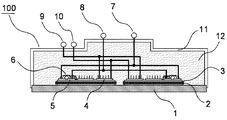
図1は、この発明を実施するための実施の形態1における電力用半導体モジュールの断面図であり、電力用半導体モジュールの断面を簡略化して示した図である。図1において、電力用半導体モジュール100は、ベース板1、絶縁基板2、導体パターン3、Si半導体で作製されたSi製スイッチング素子4、ワイドバンドギャップ半導体であるSiC半導体で作製されたSiC製ダイオード素子5、ワイヤ配線6、主電極7,8、制御端子9,10、ケース11、絶縁封止材12などによって構成されている。Si製スイッチング素子4がSi半導体素子であり、SiC製ダイオード素子5がワイドバンドギャップ半導体素子である。
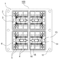
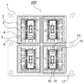
図3は、この発明を実施するための実施の形態2における電力用半導体モジュールの内部配置を示す上面図である。図2と同様に、主電極、制御端子、ケース、および絶縁封止材を外した状態で電力用半導体モジュール200を上面から見た図である。実施の形態1では、Si製スイッチング素子4が電力用半導体モジュール100の中央領域に配置され、SiC製ダイオード素子5が中央領域の両側に配置されていたが、本実施の形態では、SiC製ダイオード素子5が中央領域を囲む周辺部に配置(電力用半導体モジュール200の周辺部に配置)されている点が実施の形態1と異なる。
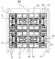
図4は、この発明を実施するための実施の形態3における電力用半導体モジュールの内部配置を示す上面図である。図2と同様に、主電極、制御端子、ケース、および絶縁封止材を外した状態で電力用半導体モジュール300を上面から見た図である。本実施の形態では、Si製スイッチング素子4とSiC製ダイオード素子5が別々の絶縁基板18,19上に実装されている点が実施の形態1と異なる。Si製スイッチング素子4は、スイッチング素子用絶縁基板18に、SiC製ダイオード素子5は、ダイオード素子用絶縁基板19にそれぞれ実装されている。また、Si製スイッチング素子4とSiC製ダイオード素子5が別々の絶縁基板18,19に実装されるため、スイッチング素子用絶縁基板18の導体パターンとダイオード素子用絶縁基板19の導体パターンを電気的に接続するワイヤ配線20を別途設けている。なお、ワイヤ配線を用いなくても、電気的に接続されれば良く、例えば、主電極7,8に直接ワイヤ配線にて接続したり、ワイヤ配線を使わずにブスバーを用いた配線にしたりしても良い。
図5は、この発明を実施するための実施の形態4における電力用半導体モジュールの内部配置を示す上面図である。図2と同様に、主電極、制御端子、ケース、および絶縁封止材を外した状態で電力用半導体モジュール400を上面から見た図である。本実施の形態では、Si製スイッチング素子4が実装されたスイッチング素子用絶縁基板18とSiC製ダイオード素子5が実装されたダイオード素子用絶縁基板19が別々のベース板21,22上に取り付けられている点が実施の形態3と異なる。Si製スイッチング素子4が実装されたスイッチング素子用絶縁基板18がスイッチング素子用ベース板21に取り付けられ、SiC製ダイオード素子5が実装されたダイオード素子用絶縁基板19は、ダイオード素子用ベース板22に取り付けられている。図5では、スイッチング素子用ベース板21の両側にダイオード素子用ベース板22が設けられている。樹脂などの断熱性材料23によってスイッチング素子用ベース板21とダイオード素子用ベース板22との間は接続されている。また、各ベース板21,22には、取り付け穴17が設けられている。
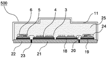
図6は、この発明を実施するための実施の形態5における電力用半導体モジュールの断面図であり、電力用半導体モジュールの断面を簡略化して示した図である。図6には、主電極および制御端子を示していない。本実施の形態における電力用半導体モジュール500では、ケース11内に充填される絶縁封止材を1種類とせずに、高耐熱絶縁封止材24および低耐熱絶縁封止材25の2種類を用いている点が実施の形態1〜4と異なる。SiC製ダイオード素子5の周辺には高耐熱絶縁封止材24を用い、それ以外の部分の、Si製スイッチング素子4の周辺などには高耐熱封止材24に比べて耐熱性の低い低耐熱絶縁封止材25を用いている。
Claims (12)
- Si半導体素子と、ワイドバンドギャップ半導体素子とを備えた電力用半導体モジュールであって、
前記Si半導体素子は、前記電力用半導体モジュールの中央領域に配置され、
前記ワイドバンドギャップ半導体素子は、前記中央領域を囲む周辺部に配置されたことを特徴とする電力用半導体モジュール。 - Si半導体素子と、ワイドバンドギャップ半導体素子とを備えた電力用半導体モジュールであって、
前記Si半導体素子は、複数の前記ワイドバンドギャップ半導体素子に囲まれるように配置されたことを特徴とする電力用半導体モジュール。 - 複数の絶縁基板と、複数のSi半導体素子と、複数のワイドバンドギャップ半導体素子とを備えた電力用半導体モジュールであって、
前記ワイドバンドギャップ半導体素子のチップサイズは、前記複数のSi半導体素子のチップサイズより小さく、
各前記複数の絶縁基板上には、複数のSi半導体素子および複数のワイドバンドギャップ半導体素子が配置されるとともに、前記絶縁基板は他の前記絶縁基板と隣接して前記電力用半導体モジュールに配置され、
前記複数のSi半導体素子が前記電力用半導体モジュールの中央領域に配置されるとともに、前記複数のワイドバンドギャップ半導体素子が前記中央領域を囲む周辺部に配置されたこと、を特徴とする電力用半導体モジュール。 - 複数の絶縁基板と、複数のSi半導体素子と、複数のワイドバンドギャップ半導体素子とを備えた電力用半導体モジュールであって、
各前記複数の絶縁基板上には、複数のSi半導体素子および複数のワイドバンドギャップ半導体素子が配置されるとともに、前記絶縁基板は他の前記絶縁基板と隣接して前記電力用半導体モジュールに配置され、
前記絶縁基板上に配置された複数のSi半導体素子および前記他の絶縁基板上に配置された複数のSi半導体素子が前記電力用半導体モジュールの中央領域に配置されるとともに、前記絶縁基板上に配置された複数のワイドバンドギャップ半導体素子と前記他の絶縁基板上に配置された複数のワイドバンドギャップ半導体素子とが前記中央領域を挟むように配置されたこと、を特徴とする電力用半導体モジュール。 - 前記Si半導体素子はスイッチング素子であり、前記ワイドバンドギャップ半導体素子はダイオード素子であることを特徴とする請求項1から4のいずれか1項に記載の電力用半導体モジュール。
- 前記Si半導体素子はダイオード素子であり、前記ワイドバンドギャップ半導体素子はスイッチング素子であることを特徴とする請求項1から4のいずれか1項に記載の電力用半導体モジュール。
- 前記Si半導体素子および前記ワイドバンドギャップ半導体素子は、それぞれ別々の絶縁基板に実装されたことを特徴とする請求項1または2に記載の電力用半導体モジュール。
- 前記Si半導体素子が実装された絶縁基板および前記ワイドバンドギャップ半導体素子が実装された絶縁基板は、同一のベース板上に設置されたことを特徴とする請求項7に記載の電力用半導体モジュール。
- 前記Si半導体素子が実装された絶縁基板および前記ワイドバンドギャップ半導体素子が実装された絶縁基板は、それぞれ別々のベース板上に設置されたことを特徴とする請求項7に記載の電力用半導体モジュール。
- 前記ワイドバンドギャップ半導体素子が配置された領域を覆う絶縁封止材は、前記Si半導体素子が配置された領域を覆う絶縁封止材よりも高耐熱特性を有することを特徴とする請求項1から9のいずれか1項に記載の電力用半導体モジュール。
- 前記ワイドバンドギャップ半導体素子が配置された領域を覆う絶縁封止材は、フッ素系樹脂、ポリイミド、ポリアミド、エポキシ、高耐熱シリコーン系樹脂のいずれかで形成され、前記Si半導体素子が配置された領域を覆う絶縁封止材は、シリコーンゲルまたはシリコーンゴムで形成されたことを特徴とする請求項1から10のいずれか1項に記載の電力用半導体モジュール。
- 前記ワイドバンドギャップ半導体素子は、シリコンカーバイト、窒化ガリウム系材料、またはダイヤモンドで作製されたことを特徴とする請求項1から11のいずれか1項に記載の電力用半導体モジュール。
Applications Claiming Priority (2)
| Application Number | Priority Date | Filing Date | Title |
|---|---|---|---|
| JP2011153020 | 2011-07-11 | ||
| JP2011153020 | 2011-07-11 |
Related Parent Applications (1)
| Application Number | Title | Priority Date | Filing Date |
|---|---|---|---|
| JP2013523812A Division JP6253409B2 (ja) | 2011-07-11 | 2012-07-05 | 電力用半導体モジュール |
Publications (2)
| Publication Number | Publication Date |
|---|---|
| JP2016167635A true JP2016167635A (ja) | 2016-09-15 |
| JP6230660B2 JP6230660B2 (ja) | 2017-11-15 |
Family
ID=47505733
Family Applications (2)
| Application Number | Title | Priority Date | Filing Date |
|---|---|---|---|
| JP2013523812A Active JP6253409B2 (ja) | 2011-07-11 | 2012-07-05 | 電力用半導体モジュール |
| JP2016114054A Active JP6230660B2 (ja) | 2011-07-11 | 2016-06-08 | 電力用半導体モジュール |
Family Applications Before (1)
| Application Number | Title | Priority Date | Filing Date |
|---|---|---|---|
| JP2013523812A Active JP6253409B2 (ja) | 2011-07-11 | 2012-07-05 | 電力用半導体モジュール |
Country Status (5)
| Country | Link |
|---|---|
| US (1) | US9299628B2 (ja) |
| EP (1) | EP2733743B1 (ja) |
| JP (2) | JP6253409B2 (ja) |
| CN (1) | CN103650137B (ja) |
| WO (1) | WO2013008424A1 (ja) |
Cited By (7)
| Publication number | Priority date | Publication date | Assignee | Title |
|---|---|---|---|---|
| JP2019016686A (ja) * | 2017-07-06 | 2019-01-31 | トヨタ自動車株式会社 | 半導体モジュール |
| WO2019064402A1 (ja) * | 2017-09-28 | 2019-04-04 | 三菱電機株式会社 | 2in1型チョッパモジュール |
| JPWO2020170553A1 (ja) * | 2019-02-18 | 2021-10-14 | 富士電機株式会社 | 半導体装置 |
| US11251163B2 (en) | 2019-12-18 | 2022-02-15 | Fuji Electric Co., Ltd. | Semiconductor device having circuit board interposed between two conductor layers |
| JP2022051499A (ja) * | 2020-09-18 | 2022-03-31 | 住友電気工業株式会社 | 半導体装置 |
| US11658231B2 (en) | 2019-12-17 | 2023-05-23 | Fuji Electric Co., Ltd. | Semiconductor device |
| US12148737B2 (en) | 2021-03-17 | 2024-11-19 | Mitsubishi Electric Corporation | Semiconductor device |
Families Citing this family (20)
| Publication number | Priority date | Publication date | Assignee | Title |
|---|---|---|---|---|
| RU2157431C2 (ru) * | 1997-07-25 | 2000-10-10 | Борик Михаил Александрович | Способ получения высокопрочного материала (варианты), устройства на основе этого материала и способ их изготовления |
| US9196604B2 (en) * | 2012-07-19 | 2015-11-24 | Mitsubishi Electric Corporation | Power semiconductor module having pattern laminated region |
| CN105247675B (zh) * | 2013-05-29 | 2019-11-15 | 三菱电机株式会社 | 半导体装置 |
| US10770985B2 (en) | 2014-07-18 | 2020-09-08 | Mitsubishi Electric Corporation | Vehicle auxiliary power supply device |
| US10224810B2 (en) * | 2015-03-16 | 2019-03-05 | Cree, Inc. | High speed, efficient SiC power module |
| US10680518B2 (en) | 2015-03-16 | 2020-06-09 | Cree, Inc. | High speed, efficient SiC power module |
| JP6524809B2 (ja) * | 2015-06-10 | 2019-06-05 | 富士電機株式会社 | 半導体装置 |
| CN105871328A (zh) * | 2016-06-03 | 2016-08-17 | 浙江人和光伏科技有限公司 | 一种太阳能电池用接线盒 |
| EP3279935B1 (en) | 2016-08-02 | 2019-01-02 | ABB Schweiz AG | Power semiconductor module |
| AU2017419197A1 (en) | 2017-06-19 | 2020-01-02 | Huawei Technologies Co., Ltd. | Registration method, session establishment method, terminal, and amf entity |
| JP6402813B2 (ja) * | 2017-09-20 | 2018-10-10 | 三菱電機株式会社 | 半導体装置 |
| WO2020059285A1 (ja) * | 2018-09-20 | 2020-03-26 | 富士電機株式会社 | 半導体装置 |
| JP7150183B2 (ja) * | 2019-08-20 | 2022-10-07 | 三菱電機株式会社 | 半導体装置、電力変換装置及び移動体 |
| EP4120336A1 (en) * | 2021-07-15 | 2023-01-18 | Infineon Technologies Austria AG | A semiconductor power module with two different potting materials and a method for fabricating the same |
| JP7710409B2 (ja) | 2022-04-04 | 2025-07-18 | 三菱電機株式会社 | 半導体装置の製造方法 |
| US12218018B2 (en) | 2022-04-21 | 2025-02-04 | Infineon Technologies Ag | Semiconductor encapsulant strength enhancer |
| EP4270453A1 (en) * | 2022-04-28 | 2023-11-01 | Infineon Technologies AG | Method for fabricating a power semiconductor module comprising an encapsulation material with a high thermostability and power semiconductor module |
| EP4270454A3 (en) * | 2022-04-28 | 2023-11-22 | Infineon Technologies AG | Power semiconductor module comprising a first and a second compartment and method for fabricating the same |
| WO2024018810A1 (ja) * | 2022-07-21 | 2024-01-25 | ローム株式会社 | 半導体装置 |
| JP7609340B1 (ja) * | 2024-04-17 | 2025-01-07 | 三菱電機株式会社 | 半導体装置 |
Citations (9)
| Publication number | Priority date | Publication date | Assignee | Title |
|---|---|---|---|---|
| JPS61112362A (ja) * | 1984-11-07 | 1986-05-30 | Hitachi Ltd | 半導体装置 |
| JPH03126055U (ja) * | 1990-03-30 | 1991-12-19 | ||
| JPH0888240A (ja) * | 1994-09-15 | 1996-04-02 | Toshiba Corp | 圧接型半導体装置 |
| JP2001245479A (ja) * | 2000-02-29 | 2001-09-07 | Mitsubishi Electric Corp | 電力半導体モジュール |
| JP2006149195A (ja) * | 1995-06-21 | 2006-06-08 | Cree Inc | 変換器回路、少なくとも1つのスイッチング・デバイスを有する回路および回路モジュール |
| JP2009021395A (ja) * | 2007-07-12 | 2009-01-29 | Panasonic Corp | 半導体装置 |
| JP2009159184A (ja) * | 2007-12-26 | 2009-07-16 | Hitachi Ltd | フリーホイールダイオードとを有する回路装置、及び、ダイオードを用いた回路装置とそれを用いた電力変換器 |
| JP2009272482A (ja) * | 2008-05-08 | 2009-11-19 | Toyota Motor Corp | 半導体装置 |
| JP2010232576A (ja) * | 2009-03-30 | 2010-10-14 | Hitachi Ltd | パワー半導体装置 |
Family Cites Families (21)
| Publication number | Priority date | Publication date | Assignee | Title |
|---|---|---|---|---|
| JPH0722364Y2 (ja) | 1988-08-31 | 1995-05-24 | 株式会社村上開明堂 | ミラーの水滴除去装置 |
| JPH03126055A (ja) * | 1989-10-11 | 1991-05-29 | Seiko Epson Corp | 電子写真記録装置の現像器ユニット |
| JPH05347377A (ja) * | 1992-06-16 | 1993-12-27 | Fuji Electric Co Ltd | 半導体装置 |
| JP3588503B2 (ja) * | 1995-06-20 | 2004-11-10 | 株式会社東芝 | 圧接型半導体装置 |
| JP3433279B2 (ja) * | 1995-11-09 | 2003-08-04 | 株式会社日立製作所 | 半導体装置 |
| JPH09186287A (ja) | 1995-12-28 | 1997-07-15 | Shindengen Electric Mfg Co Ltd | 半導体装置 |
| JPH11274482A (ja) * | 1998-03-20 | 1999-10-08 | Toshiba Corp | 半導体装置 |
| JP2000340896A (ja) | 1999-05-27 | 2000-12-08 | Kyocera Corp | 配線基板モジュール |
| JP3798184B2 (ja) * | 1999-06-09 | 2006-07-19 | 矢崎総業株式会社 | パワー半導体モジュール |
| JP3621659B2 (ja) * | 2001-05-09 | 2005-02-16 | 三菱電機株式会社 | 電力変換システム |
| JP4262453B2 (ja) * | 2002-07-15 | 2009-05-13 | 三菱電機株式会社 | 電力半導体装置 |
| JP2004095670A (ja) | 2002-08-29 | 2004-03-25 | Toshiba Corp | 半導体装置 |
| US7034345B2 (en) * | 2003-03-27 | 2006-04-25 | The Boeing Company | High-power, integrated AC switch module with distributed array of hybrid devices |
| JP2006303306A (ja) * | 2005-04-22 | 2006-11-02 | Nissan Motor Co Ltd | パワーモジュール |
| US20070152309A1 (en) * | 2005-12-29 | 2007-07-05 | Para Light Electronics Co., Ltd. | Light emitting diode |
| JP2008060430A (ja) | 2006-08-31 | 2008-03-13 | Daikin Ind Ltd | 電力変換装置 |
| CN102067309B (zh) * | 2008-07-10 | 2013-08-28 | 三菱电机株式会社 | 电力用半导体模块 |
| JP2010040569A (ja) | 2008-07-31 | 2010-02-18 | Aisin Aw Co Ltd | 電子部品モジュール |
| JP5169764B2 (ja) | 2008-11-19 | 2013-03-27 | トヨタ自動車株式会社 | 電力変換装置 |
| CN102687270A (zh) | 2010-01-15 | 2012-09-19 | 三菱电机株式会社 | 电力用半导体模块 |
| US8519519B2 (en) * | 2010-11-03 | 2013-08-27 | Freescale Semiconductor Inc. | Semiconductor device having die pads isolated from interconnect portion and method of assembling same |
-
2012
- 2012-07-05 CN CN201280034222.4A patent/CN103650137B/zh active Active
- 2012-07-05 WO PCT/JP2012/004356 patent/WO2013008424A1/ja not_active Ceased
- 2012-07-05 JP JP2013523812A patent/JP6253409B2/ja active Active
- 2012-07-05 US US14/131,581 patent/US9299628B2/en active Active
- 2012-07-05 EP EP12810615.0A patent/EP2733743B1/en active Active
-
2016
- 2016-06-08 JP JP2016114054A patent/JP6230660B2/ja active Active
Patent Citations (9)
| Publication number | Priority date | Publication date | Assignee | Title |
|---|---|---|---|---|
| JPS61112362A (ja) * | 1984-11-07 | 1986-05-30 | Hitachi Ltd | 半導体装置 |
| JPH03126055U (ja) * | 1990-03-30 | 1991-12-19 | ||
| JPH0888240A (ja) * | 1994-09-15 | 1996-04-02 | Toshiba Corp | 圧接型半導体装置 |
| JP2006149195A (ja) * | 1995-06-21 | 2006-06-08 | Cree Inc | 変換器回路、少なくとも1つのスイッチング・デバイスを有する回路および回路モジュール |
| JP2001245479A (ja) * | 2000-02-29 | 2001-09-07 | Mitsubishi Electric Corp | 電力半導体モジュール |
| JP2009021395A (ja) * | 2007-07-12 | 2009-01-29 | Panasonic Corp | 半導体装置 |
| JP2009159184A (ja) * | 2007-12-26 | 2009-07-16 | Hitachi Ltd | フリーホイールダイオードとを有する回路装置、及び、ダイオードを用いた回路装置とそれを用いた電力変換器 |
| JP2009272482A (ja) * | 2008-05-08 | 2009-11-19 | Toyota Motor Corp | 半導体装置 |
| JP2010232576A (ja) * | 2009-03-30 | 2010-10-14 | Hitachi Ltd | パワー半導体装置 |
Cited By (10)
| Publication number | Priority date | Publication date | Assignee | Title |
|---|---|---|---|---|
| JP2019016686A (ja) * | 2017-07-06 | 2019-01-31 | トヨタ自動車株式会社 | 半導体モジュール |
| WO2019064402A1 (ja) * | 2017-09-28 | 2019-04-04 | 三菱電機株式会社 | 2in1型チョッパモジュール |
| JPWO2019064402A1 (ja) * | 2017-09-28 | 2019-12-26 | 三菱電機株式会社 | 2in1型チョッパモジュール |
| JPWO2020170553A1 (ja) * | 2019-02-18 | 2021-10-14 | 富士電機株式会社 | 半導体装置 |
| JP7201066B2 (ja) | 2019-02-18 | 2023-01-10 | 富士電機株式会社 | 半導体装置 |
| US11658231B2 (en) | 2019-12-17 | 2023-05-23 | Fuji Electric Co., Ltd. | Semiconductor device |
| US11251163B2 (en) | 2019-12-18 | 2022-02-15 | Fuji Electric Co., Ltd. | Semiconductor device having circuit board interposed between two conductor layers |
| JP2022051499A (ja) * | 2020-09-18 | 2022-03-31 | 住友電気工業株式会社 | 半導体装置 |
| JP7543969B2 (ja) | 2020-09-18 | 2024-09-03 | 住友電気工業株式会社 | 半導体装置 |
| US12148737B2 (en) | 2021-03-17 | 2024-11-19 | Mitsubishi Electric Corporation | Semiconductor device |
Also Published As
| Publication number | Publication date |
|---|---|
| JP6230660B2 (ja) | 2017-11-15 |
| JP6253409B2 (ja) | 2017-12-27 |
| CN103650137A (zh) | 2014-03-19 |
| EP2733743A4 (en) | 2015-03-18 |
| EP2733743A1 (en) | 2014-05-21 |
| JPWO2013008424A1 (ja) | 2015-02-23 |
| US20140138707A1 (en) | 2014-05-22 |
| CN103650137B (zh) | 2017-09-29 |
| US9299628B2 (en) | 2016-03-29 |
| WO2013008424A1 (ja) | 2013-01-17 |
| EP2733743B1 (en) | 2022-03-16 |
Similar Documents
| Publication | Publication Date | Title |
|---|---|---|
| JP6230660B2 (ja) | 電力用半導体モジュール | |
| JP5147996B2 (ja) | 電力用半導体モジュール | |
| EP2722879B1 (en) | Semiconductor unit and semiconductor device using the same | |
| US9129931B2 (en) | Power semiconductor module and power unit device | |
| EP3288075B1 (en) | Power semiconductor module | |
| US10217690B2 (en) | Semiconductor module that have multiple paths for heat dissipation | |
| US8168985B2 (en) | Semiconductor module including a switch and non-central diode | |
| JP2015015270A (ja) | 半導体装置 | |
| US10964630B2 (en) | Semiconductor device having a conductor plate and semiconductor elements | |
| JPWO2014192093A1 (ja) | 半導体装置 | |
| JP2010177619A (ja) | 半導体モジュール | |
| JP2017054855A (ja) | 半導体装置、及び半導体パッケージ | |
| JP7103256B2 (ja) | 半導体装置 | |
| JP5078290B2 (ja) | パワー半導体モジュール | |
| JP7649186B2 (ja) | 半導体モジュール | |
| US20250112143A1 (en) | Semiconductor device, semiconductor module and manufacturing method | |
| CN101419951B (zh) | 半导体功率模块用的散热装置 | |
| CN118160091A (zh) | 用于改善的热性能的功率半导体器件的布置 |
Legal Events
| Date | Code | Title | Description |
|---|---|---|---|
| A621 | Written request for application examination |
Free format text: JAPANESE INTERMEDIATE CODE: A621 Effective date: 20160608 |
|
| A977 | Report on retrieval |
Free format text: JAPANESE INTERMEDIATE CODE: A971007 Effective date: 20170220 |
|
| A131 | Notification of reasons for refusal |
Free format text: JAPANESE INTERMEDIATE CODE: A131 Effective date: 20170228 |
|
| A521 | Request for written amendment filed |
Free format text: JAPANESE INTERMEDIATE CODE: A523 Effective date: 20170424 |
|
| TRDD | Decision of grant or rejection written | ||
| A01 | Written decision to grant a patent or to grant a registration (utility model) |
Free format text: JAPANESE INTERMEDIATE CODE: A01 Effective date: 20170919 |
|
| A61 | First payment of annual fees (during grant procedure) |
Free format text: JAPANESE INTERMEDIATE CODE: A61 Effective date: 20171017 |
|
| R151 | Written notification of patent or utility model registration |
Ref document number: 6230660 Country of ref document: JP Free format text: JAPANESE INTERMEDIATE CODE: R151 |
|
| R250 | Receipt of annual fees |
Free format text: JAPANESE INTERMEDIATE CODE: R250 |
|
| R250 | Receipt of annual fees |
Free format text: JAPANESE INTERMEDIATE CODE: R250 |
|
| R250 | Receipt of annual fees |
Free format text: JAPANESE INTERMEDIATE CODE: R250 |
|
| R250 | Receipt of annual fees |
Free format text: JAPANESE INTERMEDIATE CODE: R250 |
|
| R250 | Receipt of annual fees |
Free format text: JAPANESE INTERMEDIATE CODE: R250 |
|
| R250 | Receipt of annual fees |
Free format text: JAPANESE INTERMEDIATE CODE: R250 |