JP2016192568A - 電子部品内蔵基板 - Google Patents
電子部品内蔵基板 Download PDFInfo
- Publication number
- JP2016192568A JP2016192568A JP2016128797A JP2016128797A JP2016192568A JP 2016192568 A JP2016192568 A JP 2016192568A JP 2016128797 A JP2016128797 A JP 2016128797A JP 2016128797 A JP2016128797 A JP 2016128797A JP 2016192568 A JP2016192568 A JP 2016192568A
- Authority
- JP
- Japan
- Prior art keywords
- electronic component
- wiring
- wiring layer
- substrate according
- substrate
- Prior art date
- Legal status (The legal status is an assumption and is not a legal conclusion. Google has not performed a legal analysis and makes no representation as to the accuracy of the status listed.)
- Granted
Links
Images




Classifications
-
- H—ELECTRICITY
- H05—ELECTRIC TECHNIQUES NOT OTHERWISE PROVIDED FOR
- H05K—PRINTED CIRCUITS; CASINGS OR CONSTRUCTIONAL DETAILS OF ELECTRIC APPARATUS; MANUFACTURE OF ASSEMBLAGES OF ELECTRICAL COMPONENTS
- H05K1/00—Printed circuits
- H05K1/02—Details
- H05K1/0271—Arrangements for reducing stress or warp in rigid printed circuit boards, e.g. caused by loads, vibrations or differences in thermal expansion
-
- H—ELECTRICITY
- H05—ELECTRIC TECHNIQUES NOT OTHERWISE PROVIDED FOR
- H05K—PRINTED CIRCUITS; CASINGS OR CONSTRUCTIONAL DETAILS OF ELECTRIC APPARATUS; MANUFACTURE OF ASSEMBLAGES OF ELECTRICAL COMPONENTS
- H05K3/00—Apparatus or processes for manufacturing printed circuits
- H05K3/46—Manufacturing multilayer circuits
-
- H—ELECTRICITY
- H05—ELECTRIC TECHNIQUES NOT OTHERWISE PROVIDED FOR
- H05K—PRINTED CIRCUITS; CASINGS OR CONSTRUCTIONAL DETAILS OF ELECTRIC APPARATUS; MANUFACTURE OF ASSEMBLAGES OF ELECTRICAL COMPONENTS
- H05K1/00—Printed circuits
- H05K1/18—Printed circuits structurally associated with non-printed electric components
- H05K1/182—Printed circuits structurally associated with non-printed electric components associated with components mounted in printed circuit boards [PCB], e.g. insert-mounted components [IMC]
- H05K1/185—Printed circuits structurally associated with non-printed electric components associated with components mounted in printed circuit boards [PCB], e.g. insert-mounted components [IMC] associated with components encapsulated in the insulating substrate of the PCBs; associated with components incorporated in internal layers of multilayer circuit boards
-
- H—ELECTRICITY
- H05—ELECTRIC TECHNIQUES NOT OTHERWISE PROVIDED FOR
- H05K—PRINTED CIRCUITS; CASINGS OR CONSTRUCTIONAL DETAILS OF ELECTRIC APPARATUS; MANUFACTURE OF ASSEMBLAGES OF ELECTRICAL COMPONENTS
- H05K3/00—Apparatus or processes for manufacturing printed circuits
- H05K3/46—Manufacturing multilayer circuits
- H05K3/4697—Manufacturing multilayer circuits having cavities, e.g. for mounting components
-
- H—ELECTRICITY
- H05—ELECTRIC TECHNIQUES NOT OTHERWISE PROVIDED FOR
- H05K—PRINTED CIRCUITS; CASINGS OR CONSTRUCTIONAL DETAILS OF ELECTRIC APPARATUS; MANUFACTURE OF ASSEMBLAGES OF ELECTRICAL COMPONENTS
- H05K2201/00—Indexing scheme relating to printed circuits covered by H05K1/00
- H05K2201/06—Thermal details
- H05K2201/068—Thermal details wherein the coefficient of thermal expansion is important
-
- H—ELECTRICITY
- H10—SEMICONDUCTOR DEVICES; ELECTRIC SOLID-STATE DEVICES NOT OTHERWISE PROVIDED FOR
- H10W—GENERIC PACKAGES, INTERCONNECTIONS, CONNECTORS OR OTHER CONSTRUCTIONAL DETAILS OF DEVICES COVERED BY CLASS H10
- H10W70/00—Package substrates; Interposers; Redistribution layers [RDL]
- H10W70/01—Manufacture or treatment
- H10W70/05—Manufacture or treatment of insulating or insulated package substrates, or of interposers, or of redistribution layers
- H10W70/08—Manufacture or treatment of insulating or insulated package substrates, or of interposers, or of redistribution layers by depositing layers on the chip or wafer, e.g. "chip-first" RDLs
- H10W70/09—Manufacture or treatment of insulating or insulated package substrates, or of interposers, or of redistribution layers by depositing layers on the chip or wafer, e.g. "chip-first" RDLs extending onto an encapsulation that laterally surrounds the chip or wafer, e.g. fan-out wafer level package [FOWLP] RDLs
-
- H—ELECTRICITY
- H10—SEMICONDUCTOR DEVICES; ELECTRIC SOLID-STATE DEVICES NOT OTHERWISE PROVIDED FOR
- H10W—GENERIC PACKAGES, INTERCONNECTIONS, CONNECTORS OR OTHER CONSTRUCTIONAL DETAILS OF DEVICES COVERED BY CLASS H10
- H10W70/00—Package substrates; Interposers; Redistribution layers [RDL]
- H10W70/099—Connecting interconnections to insulating or insulated package substrates, interposers or redistribution layers
-
- H—ELECTRICITY
- H10—SEMICONDUCTOR DEVICES; ELECTRIC SOLID-STATE DEVICES NOT OTHERWISE PROVIDED FOR
- H10W—GENERIC PACKAGES, INTERCONNECTIONS, CONNECTORS OR OTHER CONSTRUCTIONAL DETAILS OF DEVICES COVERED BY CLASS H10
- H10W70/00—Package substrates; Interposers; Redistribution layers [RDL]
- H10W70/60—Insulating or insulated package substrates; Interposers; Redistribution layers
-
- H—ELECTRICITY
- H10—SEMICONDUCTOR DEVICES; ELECTRIC SOLID-STATE DEVICES NOT OTHERWISE PROVIDED FOR
- H10W—GENERIC PACKAGES, INTERCONNECTIONS, CONNECTORS OR OTHER CONSTRUCTIONAL DETAILS OF DEVICES COVERED BY CLASS H10
- H10W70/00—Package substrates; Interposers; Redistribution layers [RDL]
- H10W70/60—Insulating or insulated package substrates; Interposers; Redistribution layers
- H10W70/67—Insulating or insulated package substrates; Interposers; Redistribution layers characterised by their insulating layers or insulating parts
- H10W70/68—Shapes or dispositions thereof
- H10W70/682—Shapes or dispositions thereof comprising holes having chips therein
-
- H—ELECTRICITY
- H10—SEMICONDUCTOR DEVICES; ELECTRIC SOLID-STATE DEVICES NOT OTHERWISE PROVIDED FOR
- H10W—GENERIC PACKAGES, INTERCONNECTIONS, CONNECTORS OR OTHER CONSTRUCTIONAL DETAILS OF DEVICES COVERED BY CLASS H10
- H10W72/00—Interconnections or connectors in packages
- H10W72/071—Connecting or disconnecting
- H10W72/073—Connecting or disconnecting of die-attach connectors
-
- H—ELECTRICITY
- H10—SEMICONDUCTOR DEVICES; ELECTRIC SOLID-STATE DEVICES NOT OTHERWISE PROVIDED FOR
- H10W—GENERIC PACKAGES, INTERCONNECTIONS, CONNECTORS OR OTHER CONSTRUCTIONAL DETAILS OF DEVICES COVERED BY CLASS H10
- H10W72/00—Interconnections or connectors in packages
- H10W72/071—Connecting or disconnecting
- H10W72/073—Connecting or disconnecting of die-attach connectors
- H10W72/07302—Connecting or disconnecting of die-attach connectors using an auxiliary member
- H10W72/07304—Connecting or disconnecting of die-attach connectors using an auxiliary member the auxiliary member being temporary, e.g. a sacrificial coating
- H10W72/07307—Connecting or disconnecting of die-attach connectors using an auxiliary member the auxiliary member being temporary, e.g. a sacrificial coating the auxiliary member being a temporary substrate, e.g. a removable substrate
-
- H—ELECTRICITY
- H10—SEMICONDUCTOR DEVICES; ELECTRIC SOLID-STATE DEVICES NOT OTHERWISE PROVIDED FOR
- H10W—GENERIC PACKAGES, INTERCONNECTIONS, CONNECTORS OR OTHER CONSTRUCTIONAL DETAILS OF DEVICES COVERED BY CLASS H10
- H10W72/00—Interconnections or connectors in packages
- H10W72/20—Bump connectors, e.g. solder bumps or copper pillars; Dummy bumps; Thermal bumps
- H10W72/241—Dispositions, e.g. layouts
-
- H—ELECTRICITY
- H10—SEMICONDUCTOR DEVICES; ELECTRIC SOLID-STATE DEVICES NOT OTHERWISE PROVIDED FOR
- H10W—GENERIC PACKAGES, INTERCONNECTIONS, CONNECTORS OR OTHER CONSTRUCTIONAL DETAILS OF DEVICES COVERED BY CLASS H10
- H10W72/00—Interconnections or connectors in packages
- H10W72/851—Dispositions of multiple connectors or interconnections
- H10W72/874—On different surfaces
-
- H—ELECTRICITY
- H10—SEMICONDUCTOR DEVICES; ELECTRIC SOLID-STATE DEVICES NOT OTHERWISE PROVIDED FOR
- H10W—GENERIC PACKAGES, INTERCONNECTIONS, CONNECTORS OR OTHER CONSTRUCTIONAL DETAILS OF DEVICES COVERED BY CLASS H10
- H10W72/00—Interconnections or connectors in packages
- H10W72/90—Bond pads, in general
- H10W72/941—Dispositions of bond pads
- H10W72/9413—Dispositions of bond pads on encapsulations
-
- H—ELECTRICITY
- H10—SEMICONDUCTOR DEVICES; ELECTRIC SOLID-STATE DEVICES NOT OTHERWISE PROVIDED FOR
- H10W—GENERIC PACKAGES, INTERCONNECTIONS, CONNECTORS OR OTHER CONSTRUCTIONAL DETAILS OF DEVICES COVERED BY CLASS H10
- H10W72/00—Interconnections or connectors in packages
- H10W72/90—Bond pads, in general
- H10W72/941—Dispositions of bond pads
- H10W72/942—Dispositions of bond pads relative to underlying supporting features, e.g. bond pads, RDLs or vias
-
- H—ELECTRICITY
- H10—SEMICONDUCTOR DEVICES; ELECTRIC SOLID-STATE DEVICES NOT OTHERWISE PROVIDED FOR
- H10W—GENERIC PACKAGES, INTERCONNECTIONS, CONNECTORS OR OTHER CONSTRUCTIONAL DETAILS OF DEVICES COVERED BY CLASS H10
- H10W72/00—Interconnections or connectors in packages
- H10W72/90—Bond pads, in general
- H10W72/941—Dispositions of bond pads
- H10W72/944—Dispositions of multiple bond pads
-
- H—ELECTRICITY
- H10—SEMICONDUCTOR DEVICES; ELECTRIC SOLID-STATE DEVICES NOT OTHERWISE PROVIDED FOR
- H10W—GENERIC PACKAGES, INTERCONNECTIONS, CONNECTORS OR OTHER CONSTRUCTIONAL DETAILS OF DEVICES COVERED BY CLASS H10
- H10W90/00—Package configurations
- H10W90/701—Package configurations characterised by the relative positions of pads or connectors relative to package parts
- H10W90/721—Package configurations characterised by the relative positions of pads or connectors relative to package parts of bump connectors
- H10W90/724—Package configurations characterised by the relative positions of pads or connectors relative to package parts of bump connectors between a chip and a stacked insulating package substrate, interposer or RDL
-
- H—ELECTRICITY
- H10—SEMICONDUCTOR DEVICES; ELECTRIC SOLID-STATE DEVICES NOT OTHERWISE PROVIDED FOR
- H10W—GENERIC PACKAGES, INTERCONNECTIONS, CONNECTORS OR OTHER CONSTRUCTIONAL DETAILS OF DEVICES COVERED BY CLASS H10
- H10W90/00—Package configurations
- H10W90/701—Package configurations characterised by the relative positions of pads or connectors relative to package parts
- H10W90/731—Package configurations characterised by the relative positions of pads or connectors relative to package parts of die-attach connectors
- H10W90/734—Package configurations characterised by the relative positions of pads or connectors relative to package parts of die-attach connectors between a chip and a stacked insulating package substrate, interposer or RDL
-
- H—ELECTRICITY
- H10—SEMICONDUCTOR DEVICES; ELECTRIC SOLID-STATE DEVICES NOT OTHERWISE PROVIDED FOR
- H10W—GENERIC PACKAGES, INTERCONNECTIONS, CONNECTORS OR OTHER CONSTRUCTIONAL DETAILS OF DEVICES COVERED BY CLASS H10
- H10W90/00—Package configurations
- H10W90/701—Package configurations characterised by the relative positions of pads or connectors relative to package parts
- H10W90/731—Package configurations characterised by the relative positions of pads or connectors relative to package parts of die-attach connectors
- H10W90/736—Package configurations characterised by the relative positions of pads or connectors relative to package parts of die-attach connectors between a chip and a stacked lead frame, conducting package substrate or heat sink
-
- Y—GENERAL TAGGING OF NEW TECHNOLOGICAL DEVELOPMENTS; GENERAL TAGGING OF CROSS-SECTIONAL TECHNOLOGIES SPANNING OVER SEVERAL SECTIONS OF THE IPC; TECHNICAL SUBJECTS COVERED BY FORMER USPC CROSS-REFERENCE ART COLLECTIONS [XRACs] AND DIGESTS
- Y10—TECHNICAL SUBJECTS COVERED BY FORMER USPC
- Y10T—TECHNICAL SUBJECTS COVERED BY FORMER US CLASSIFICATION
- Y10T156/00—Adhesive bonding and miscellaneous chemical manufacture
- Y10T156/10—Methods of surface bonding and/or assembly therefor
-
- Y—GENERAL TAGGING OF NEW TECHNOLOGICAL DEVELOPMENTS; GENERAL TAGGING OF CROSS-SECTIONAL TECHNOLOGIES SPANNING OVER SEVERAL SECTIONS OF THE IPC; TECHNICAL SUBJECTS COVERED BY FORMER USPC CROSS-REFERENCE ART COLLECTIONS [XRACs] AND DIGESTS
- Y10—TECHNICAL SUBJECTS COVERED BY FORMER USPC
- Y10T—TECHNICAL SUBJECTS COVERED BY FORMER US CLASSIFICATION
- Y10T29/00—Metal working
- Y10T29/49—Method of mechanical manufacture
- Y10T29/49002—Electrical device making
- Y10T29/49117—Conductor or circuit manufacturing
- Y10T29/49124—On flat or curved insulated base, e.g., printed circuit, etc.
- Y10T29/4913—Assembling to base an electrical component, e.g., capacitor, etc.
- Y10T29/49139—Assembling to base an electrical component, e.g., capacitor, etc. by inserting component lead or terminal into base aperture
Landscapes
- Engineering & Computer Science (AREA)
- Microelectronics & Electronic Packaging (AREA)
- Manufacturing & Machinery (AREA)
- Production Of Multi-Layered Print Wiring Board (AREA)
Abstract
Description
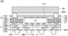
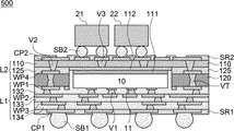
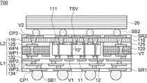
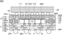
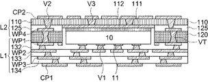
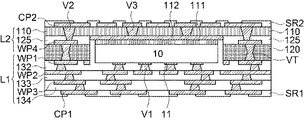
第1の配線層L1は、電子部品10を基準に第1の外部端子11の各々から遠くなる方向に設けられ、第1の配線及び第1の絶縁部を有する。第1の配線層L1は、第1の外部端子11を基板の内部、または外部の他のデバイスと電気的に接続される。
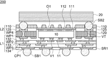
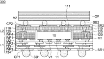
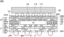
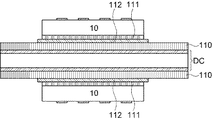
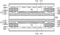
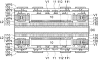
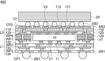
10 電子部品
11 第1の外部端子
12 第2の外部端子
20、21、22 チップ部品
110 絶縁基板
111 接着部材
112 第1の金属パターン
120 第1の絶縁層
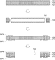
122 キャビティ
125 第5の絶縁層
132 第2の絶縁層
133 第3の絶縁層
134 第4の絶縁層
WP1 第1の配線パターン
WP2 第2の配線パターン
WP3 第3の配線パターン
WP4 第4の配線パターン
CP1 第1の接触パッド
CP2 第2の接触パッド
SR1 第1のソルダレジスト
SR2 第2のソルダレジスト
SB1 第1のソルダボール
SB2 第2のソルダボール
SB3 第3のソルダボール
O1 第1の開口部
O2 第2の開口部
L1 第1の配線層
L2 第2の配線層
VT スルービア
DC ディタッチコア
TSV スルーシリコーンビア
Claims (25)
- 第1の外部端子が複数設けられる第1の面、及び該第1の面の反対側の面であって絶縁物質からなる第2の面を備える電子部品と、
前記第1の面上に設けられ、前記第1の外部端子と電気的に接続される第1の配線及び第1の絶縁部を備える第1の配線層と、
前記第2の面上に設けられ、第2の配線及び第2の絶縁部を備える第2の配線層とを含み、
前記第1の配線層の層数は、前記第2の配線層の層数より大きく、
前記第1の配線層の配線密度は、前記第2の配線層の配線密度より高く、
前記第1の絶縁部は、前記第2の絶縁部より熱膨脹係数が低い物質からなることを特徴とする電子部品内蔵基板。 - 前記電子部品の少なくとも一部が挿入されるキャビティを含み、絶縁材料からなる第1の絶縁層をさらに含むことを特徴とする請求項1に記載の電子部品内蔵基板。
- 前記第1の絶縁層は、コア基板であることを特徴とする請求項2に記載の電子部品内蔵基板。
- 前記第1の絶縁層を貫いて前記第1の配線層及び前記第2の配線層を電気的に接続するスルービアを、さらに含むことを特徴とする請求項3に記載の電子部品内蔵基板。
- 前記第1の配線層の外面には、前記第1の配線と電気的に接続される第1の接触パッドがさらに設けられることを特徴とする請求項1に記載の電子部品内蔵基板。
- 前記第1の配線層の外面には、前記第1の接触パッドを外部に露出させる第1のソルダレジストが、さらに設けられることを特徴とする請求項5に記載の電子部品内蔵基板。
- 前記電子部品の第2の面に接触する接着部材を、さらに含むことを特徴とする請求項1に記載の電子部品内蔵基板。
- 前記接着部材の外面に設けられる複数の第1の金属パターンを、さらに含むことを特徴とする請求項7に記載の電子部品内蔵基板。
- 前記第2の配線層上に設けられ、前記第2の配線層と電気的に接続されるチップ部品を、さらに含むことを特徴とする請求項1に記載の電子部品内蔵基板。
- 前記チップ部品はメモリーチップであり、前記電子部品は集積回路であることを特徴とする請求項9に記載の電子部品内蔵基板。
- 前記第2の配線層の外面には、前記第2の配線と電気的に接続される第2の接触パッドが、さらに設けられることを特徴とする請求項9に記載の電子部品内蔵基板。
- 前記第2の接触パッドと前記チップ部品とを電気的に接続するソルダボールを、さらに含むことを特徴とする請求項11に記載の電子部品内蔵基板。
- 前記ソルダボールは、前記電子部品の垂直上方または垂直下方の領域に設けられることを特徴とする請求項12に記載の電子部品内蔵基板。
- 前記第2の配線層の外面には、前記第2の接触パッドを外部に露出させる第2のソルダレジストが、さらに設けられることを特徴とする請求項11に記載の電子部品内蔵基板。
- 第1の外部端子が複数設けられる第1の面、及び該第1の面の反対側の面であって第2の外部端子が少なくとも一つ設けられる第2の面を備える電子部品と、
前記第1の面上に設けられ、前記第1の外部端子と電気的に接続される第1の配線及び第1の絶縁部を備える第1の配線層と、
前記第2の面上に設けられ、前記第2の外部端子と電気的に接続される第2の配線及び第2の絶縁部を備える第2の配線層とを含み、
前記第2の外部端子の数は、前記第1の外部端子の数より少なく、
前記第1の配線層の層数は、前記第2の配線層の層数より大きく、
前記第1の配線層の配線密度は、前記第2の配線層の配線密度より高く、
前記第1の絶縁部は、前記第2の絶縁部より熱膨脹係数が低い物質からなることを特徴とする電子部品内蔵基板。 - 前記第2の配線層上に設けられ、前記第2の配線層と電気的に接続されるチップ部品を、さらに含むことを特徴とする請求項15に記載の電子部品内蔵基板。
- 前記チップ部品はメモリーチップであり、前記電子部品は集積回路であることを特徴とする請求項16に記載の電子部品内蔵基板。
- 前記第2の配線層の外面には、前記第2の配線と電気的に接続される第2の接触パッドが、さらに設けられることを特徴とする請求項16に記載の電子部品内蔵基板。
- 前記第2の接触パッドと前記チップ部品とを電気的に接続するソルダボールを、さらに含むことを特徴とする請求項18に記載の電子部品内蔵基板。
- 前記ソルダボールは、前記電子部品の垂直上方または垂直下方の領域に設けられることを特徴とする請求項19に記載の電子部品内蔵基板。
- 前記第2の配線層の外面に設けられ、前記第2の接触パッドを外部に露出させる第2のソルダレジストを、さらに含むことを特徴とする請求項18に記載の電子部品内蔵基板。
- 前記第1の外部端子と前記第2の外部端子とは前記電子部品を貫くスルーシリコーンビアによって電気的に接続されることを特徴とする請求項15に記載の電子部品内蔵基板。
- 前記第2の配線層は、前記第2の外部端子に一面が接触されるビアを含むことを特徴とする請求項22に記載の電子部品内蔵基板。
- 前記第2の配線層の外面には前記ビアの他面に接触される第2の接触パッドと、
ソルダボールによって前記第2の接触パッドに電気的に接続されるチップ部品と、をさらに含むことを特徴とする請求項23に記載の電子部品内蔵基板。 - 前記電子部品の第2の面に接触する接着部材と、
前記接着部材の外面に設けられる複数の第1の金属パターンと、
前記第1の金属パターン各々に一面が接触される少なくとも一つのビアと、
前記ビアの他面に接触される第2の接触パッドと、
ソルダボールによって前記第2の接触パッドに電気的に接続されるチップ部品と、をさらに含み、
前記複数の第1の金属パターン及び前記第2の外部端子は、第2のソルダボールによって電気的に接続されることを特徴とする請求項22に記載の電子部品内蔵基板。
Applications Claiming Priority (2)
| Application Number | Priority Date | Filing Date | Title |
|---|---|---|---|
| KR10-2013-0103276 | 2013-08-29 | ||
| KR1020130103276A KR101514539B1 (ko) | 2013-08-29 | 2013-08-29 | 전자부품 내장기판 |
Related Parent Applications (1)
| Application Number | Title | Priority Date | Filing Date |
|---|---|---|---|
| JP2014043573A Division JP6023107B2 (ja) | 2013-08-29 | 2014-03-06 | 電子部品内蔵基板及びその製造方法 |
Publications (3)
| Publication Number | Publication Date |
|---|---|
| JP2016192568A true JP2016192568A (ja) | 2016-11-10 |
| JP2016192568A5 JP2016192568A5 (ja) | 2017-03-30 |
| JP6325605B2 JP6325605B2 (ja) | 2018-05-16 |
Family
ID=52582969
Family Applications (2)
| Application Number | Title | Priority Date | Filing Date |
|---|---|---|---|
| JP2014043573A Expired - Fee Related JP6023107B2 (ja) | 2013-08-29 | 2014-03-06 | 電子部品内蔵基板及びその製造方法 |
| JP2016128797A Expired - Fee Related JP6325605B2 (ja) | 2013-08-29 | 2016-06-29 | 電子部品内蔵基板 |
Family Applications Before (1)
| Application Number | Title | Priority Date | Filing Date |
|---|---|---|---|
| JP2014043573A Expired - Fee Related JP6023107B2 (ja) | 2013-08-29 | 2014-03-06 | 電子部品内蔵基板及びその製造方法 |
Country Status (3)
| Country | Link |
|---|---|
| US (1) | US9516740B2 (ja) |
| JP (2) | JP6023107B2 (ja) |
| KR (1) | KR101514539B1 (ja) |
Families Citing this family (42)
| Publication number | Priority date | Publication date | Assignee | Title |
|---|---|---|---|---|
| KR20150074785A (ko) * | 2013-12-24 | 2015-07-02 | 삼성전기주식회사 | 빌드업 절연필름, 그를 이용한 전자부품 내장형 인쇄회로기판 및 그 제조방법 |
| KR102186149B1 (ko) * | 2015-03-11 | 2020-12-03 | 삼성전기주식회사 | 인쇄회로기판 및 그의 제조 방법 |
| KR102426528B1 (ko) * | 2015-04-14 | 2022-07-29 | 엘지이노텍 주식회사 | 임베디드 인쇄회로기판 |
| US9984979B2 (en) | 2015-05-11 | 2018-05-29 | Samsung Electro-Mechanics Co., Ltd. | Fan-out semiconductor package and method of manufacturing the same |
| US10199337B2 (en) | 2015-05-11 | 2019-02-05 | Samsung Electro-Mechanics Co., Ltd. | Electronic component package and method of manufacturing the same |
| KR20160132751A (ko) * | 2015-05-11 | 2016-11-21 | 삼성전기주식회사 | 전자부품 패키지 및 그 제조방법 |
| KR102595276B1 (ko) * | 2016-01-14 | 2023-10-31 | 삼성전자주식회사 | 반도체 패키지 |
| KR102656394B1 (ko) * | 2016-08-18 | 2024-04-11 | 삼성전기주식회사 | 반도체 패키지 및 이를 이용한 전자소자 모듈 |
| JP2018078274A (ja) * | 2016-11-10 | 2018-05-17 | サムソン エレクトロ−メカニックス カンパニーリミテッド. | イメージセンサー装置及びそれを含むイメージセンサーモジュール |
| CN110024116A (zh) * | 2016-12-27 | 2019-07-16 | 英特尔公司 | 堆叠管芯腔封装 |
| KR102426202B1 (ko) * | 2017-01-09 | 2022-07-29 | 삼성전기주식회사 | 인쇄회로기판 |
| JP7383866B2 (ja) * | 2017-01-09 | 2023-11-21 | サムソン エレクトロ-メカニックス カンパニーリミテッド. | プリント回路基板 |
| JP6862886B2 (ja) * | 2017-02-13 | 2021-04-21 | Tdk株式会社 | 電子部品内蔵基板 |
| EP3373714B1 (en) * | 2017-03-08 | 2023-08-23 | AT & S Austria Technologie & Systemtechnik Aktiengesellschaft | Hybrid component carrier and method for manufacturing the same |
| CN111149199A (zh) | 2017-10-11 | 2020-05-12 | 索尼半导体解决方案公司 | 半导体装置及其制造方法 |
| KR101939046B1 (ko) * | 2017-10-31 | 2019-01-16 | 삼성전기 주식회사 | 팬-아웃 반도체 패키지 |
| TWI736780B (zh) | 2017-10-31 | 2021-08-21 | 台灣積體電路製造股份有限公司 | 晶片封裝及其形成方法 |
| US11322449B2 (en) | 2017-10-31 | 2022-05-03 | Taiwan Semiconductor Manufacturing Co., Ltd. | Package with fan-out structures |
| EP3483921B1 (en) | 2017-11-11 | 2026-01-07 | AT & S Austria Technologie & Systemtechnik Aktiengesellschaft | Embedding known-good component in known-good cavity of known-good component carrier material with pre-formed electric connection structure |
| JP7046639B2 (ja) * | 2018-02-21 | 2022-04-04 | 新光電気工業株式会社 | 配線基板及びその製造方法 |
| US10797017B2 (en) * | 2018-03-20 | 2020-10-06 | Unimicron Technology Corp. | Embedded chip package, manufacturing method thereof, and package-on-package structure |
| KR102164793B1 (ko) * | 2018-08-16 | 2020-10-14 | 삼성전자주식회사 | 수동부품 내장기판 |
| US10998247B2 (en) | 2018-08-16 | 2021-05-04 | Samsung Electronics Co., Ltd. | Board with embedded passive component |
| CN109300882A (zh) * | 2018-09-20 | 2019-02-01 | 蔡亲佳 | 堆叠嵌入式封装结构及其制作方法 |
| DE102019117844A1 (de) | 2018-09-27 | 2020-04-02 | Taiwan Semiconductor Manufacturing Co., Ltd. | Integrierte-schaltung-package und verfahren |
| US10790162B2 (en) * | 2018-09-27 | 2020-09-29 | Taiwan Semiconductor Manufacturing Company, Ltd. | Integrated circuit package and method |
| KR102540829B1 (ko) * | 2018-10-05 | 2023-06-08 | 삼성전자주식회사 | 반도체 패키지, 반도체 패키지 제조방법 및 재배선 구조체 제조방법 |
| KR102595864B1 (ko) * | 2018-12-07 | 2023-10-30 | 삼성전자주식회사 | 반도체 패키지 |
| KR102170904B1 (ko) * | 2018-12-21 | 2020-10-29 | 주식회사 심텍 | 수동 소자를 구비하는 인쇄회로기판 및 그 제조 방법 |
| KR102730504B1 (ko) | 2019-03-05 | 2024-11-14 | 에스케이하이닉스 주식회사 | 테스트방법 및 이를 이용한 반도체칩 |
| CN112770495B (zh) * | 2019-10-21 | 2022-05-27 | 宏启胜精密电子(秦皇岛)有限公司 | 全向内埋模组及制作方法、封装结构及制作方法 |
| KR102776264B1 (ko) * | 2019-12-19 | 2025-03-07 | 삼성전기주식회사 | 전자부품 내장기판 |
| KR102776276B1 (ko) * | 2019-12-19 | 2025-03-07 | 삼성전기주식회사 | 전자부품 내장기판 |
| JP7496251B2 (ja) * | 2020-06-19 | 2024-06-06 | イビデン株式会社 | 部品内蔵配線基板及び部品内蔵配線基板の製造方法 |
| US11348874B2 (en) * | 2020-07-08 | 2022-05-31 | Taiwan Semiconductor Manufacturing Company, Ltd. | Semiconductor packages and forming methods thereof |
| KR102854180B1 (ko) * | 2020-07-27 | 2025-09-03 | 삼성전기주식회사 | 전자부품 내장기판 |
| KR102576178B1 (ko) * | 2021-07-14 | 2023-09-07 | 주식회사 티에스이 | 테스트 소켓, 그 테스트 소켓을 포함하는 테스트 장치, 및 그 테스트 소켓 제조방법 |
| US12100645B2 (en) * | 2021-09-23 | 2024-09-24 | Qualcomm Incorporated | Integrated circuit (IC) package employing added metal for embedded metal traces in ETS-based substrate for reduced signal path impedance, and related fabrication methods |
| US12362269B2 (en) | 2021-10-18 | 2025-07-15 | Qualcomm Incorporated | Integrated circuit (IC) packages employing supplemental metal layer coupled to embedded metal traces in a die-side embedded trace substrate (ETS) layer, and related fabrication methods |
| CN116033645A (zh) | 2021-10-26 | 2023-04-28 | 奥特斯奥地利科技与系统技术有限公司 | 无芯部件承载件及用于制造无芯部件承载件的方法 |
| CN116994964A (zh) * | 2022-04-25 | 2023-11-03 | 宏启胜精密电子(秦皇岛)有限公司 | 封装结构及其制备方法 |
| JP2024109396A (ja) * | 2023-02-01 | 2024-08-14 | イビデン株式会社 | 配線基板 |
Citations (4)
| Publication number | Priority date | Publication date | Assignee | Title |
|---|---|---|---|---|
| JP2008288298A (ja) * | 2007-05-16 | 2008-11-27 | Toppan Printing Co Ltd | 電子部品を内蔵したプリント配線板の製造方法 |
| JP2011249457A (ja) * | 2010-05-25 | 2011-12-08 | Dainippon Printing Co Ltd | 部品内蔵配線板、部品内蔵配線板の製造方法 |
| JP2012069863A (ja) * | 2010-09-27 | 2012-04-05 | Nec Corp | 配線基板及びその製造方法 |
| JP2013135113A (ja) * | 2011-12-27 | 2013-07-08 | Fujikura Ltd | 部品内蔵基板の製造方法 |
Family Cites Families (15)
| Publication number | Priority date | Publication date | Assignee | Title |
|---|---|---|---|---|
| JP3672169B2 (ja) | 1999-03-05 | 2005-07-13 | 日本特殊陶業株式会社 | コンデンサ、コア基板本体の製造方法、及び、コンデンサ内蔵コア基板の製造方法 |
| EP1139705B1 (en) | 1999-09-02 | 2006-11-22 | Ibiden Co., Ltd. | Printed wiring board and method of producing the same |
| TW511405B (en) * | 2000-12-27 | 2002-11-21 | Matsushita Electric Industrial Co Ltd | Device built-in module and manufacturing method thereof |
| TWI407870B (zh) * | 2006-04-25 | 2013-09-01 | 日本特殊陶業股份有限公司 | 配線基板之製造方法 |
| US7936567B2 (en) * | 2007-05-07 | 2011-05-03 | Ngk Spark Plug Co., Ltd. | Wiring board with built-in component and method for manufacturing the same |
| JP2010114434A (ja) * | 2008-10-08 | 2010-05-20 | Ngk Spark Plug Co Ltd | 部品内蔵配線基板及びその製造方法 |
| US7935570B2 (en) * | 2008-12-10 | 2011-05-03 | Stats Chippac, Ltd. | Semiconductor device and method of embedding integrated passive devices into the package electrically interconnected using conductive pillars |
| WO2010101163A1 (ja) | 2009-03-04 | 2010-09-10 | 日本電気株式会社 | 機能素子内蔵基板及びそれを用いた電子デバイス |
| KR101077410B1 (ko) | 2009-05-15 | 2011-10-26 | 삼성전기주식회사 | 방열부재를 구비한 전자부품 내장형 인쇄회로기판 및 그 제조방법 |
| JP2011187830A (ja) | 2010-03-10 | 2011-09-22 | Tdk Corp | 電子部品内蔵基板及びその製造方法 |
| JP5605429B2 (ja) * | 2010-04-08 | 2014-10-15 | 日本電気株式会社 | 半導体素子内蔵配線基板 |
| TWI446497B (zh) * | 2010-08-13 | 2014-07-21 | 欣興電子股份有限公司 | 嵌埋被動元件之封裝基板及其製法 |
| KR101282965B1 (ko) | 2010-11-05 | 2013-07-08 | 주식회사 두산 | 신규 인쇄회로기판 및 이의 제조방법 |
| JP5439560B2 (ja) | 2012-08-10 | 2014-03-12 | 太陽誘電株式会社 | 複合多層基板およびそれを用いたモジュール |
| DE112013006630T5 (de) * | 2013-02-08 | 2015-10-22 | Fujikura Ltd. | Platte mit eingebetteter Komponente und Verfahren zum Herstellen derselben |
-
2013
- 2013-08-29 KR KR1020130103276A patent/KR101514539B1/ko not_active Expired - Fee Related
- 2013-12-17 US US14/108,517 patent/US9516740B2/en active Active
-
2014
- 2014-03-06 JP JP2014043573A patent/JP6023107B2/ja not_active Expired - Fee Related
-
2016
- 2016-06-29 JP JP2016128797A patent/JP6325605B2/ja not_active Expired - Fee Related
Patent Citations (4)
| Publication number | Priority date | Publication date | Assignee | Title |
|---|---|---|---|---|
| JP2008288298A (ja) * | 2007-05-16 | 2008-11-27 | Toppan Printing Co Ltd | 電子部品を内蔵したプリント配線板の製造方法 |
| JP2011249457A (ja) * | 2010-05-25 | 2011-12-08 | Dainippon Printing Co Ltd | 部品内蔵配線板、部品内蔵配線板の製造方法 |
| JP2012069863A (ja) * | 2010-09-27 | 2012-04-05 | Nec Corp | 配線基板及びその製造方法 |
| JP2013135113A (ja) * | 2011-12-27 | 2013-07-08 | Fujikura Ltd | 部品内蔵基板の製造方法 |
Also Published As
| Publication number | Publication date |
|---|---|
| JP6023107B2 (ja) | 2016-11-09 |
| US20150062848A1 (en) | 2015-03-05 |
| JP2015050457A (ja) | 2015-03-16 |
| US9516740B2 (en) | 2016-12-06 |
| JP6325605B2 (ja) | 2018-05-16 |
| KR20150025449A (ko) | 2015-03-10 |
| KR101514539B1 (ko) | 2015-04-22 |
Similar Documents
| Publication | Publication Date | Title |
|---|---|---|
| JP6325605B2 (ja) | 電子部品内蔵基板 | |
| JP5018483B2 (ja) | 電子デバイスパッケージ、モジュール、および電子機器 | |
| JP5224845B2 (ja) | 半導体装置の製造方法及び半導体装置 | |
| JP6083152B2 (ja) | 配線基板及び配線基板の製造方法 | |
| KR101095161B1 (ko) | 전자부품 내장형 인쇄회로기판 | |
| US7754538B2 (en) | Packaging substrate structure with electronic components embedded therein and method for manufacturing the same | |
| JP2004064043A (ja) | 半導体パッケージング装置 | |
| TWI898016B (zh) | 使用一蓋子與硬化結構封裝堆疊基板及積體電路晶粒 | |
| JP2017123459A (ja) | プリント回路基板 | |
| KR102134933B1 (ko) | 배선 기판 및 배선 기판의 제조 방법 | |
| JP6742682B2 (ja) | 多層配線基板 | |
| US20250227857A1 (en) | Manufacturing method of circuit carrier | |
| JP2016063199A (ja) | パッケージ基板 | |
| JP5660462B2 (ja) | プリント配線板 | |
| JP2001230515A (ja) | 電子部品の実装体、電子部品の実装体の製造方法、および実装体の二次実装構造。 | |
| JP6378616B2 (ja) | 電子部品内蔵プリント配線板 | |
| US8829361B2 (en) | Wiring board and mounting structure using the same | |
| JP2011155199A (ja) | 回路実装基板 | |
| JP4952365B2 (ja) | 両面実装回路基板に対する電子部品の実装構造、半導体装置、及び両面実装半導体装置の製造方法 | |
| JP2008205290A (ja) | 部品内蔵基板及びその製造方法 | |
| KR20110039879A (ko) | 전자부품 내장형 인쇄회로기판 및 그 제조방법 | |
| JP2005340355A (ja) | 配線基板 | |
| JP2004214286A (ja) | 部品内蔵モジュール | |
| TWI420989B (zh) | 印刷電路板及其製造方法 | |
| JP2008153482A (ja) | インターポーザ基板を備えた半導体パッケージ |
Legal Events
| Date | Code | Title | Description |
|---|---|---|---|
| A521 | Request for written amendment filed |
Free format text: JAPANESE INTERMEDIATE CODE: A523 Effective date: 20170224 |
|
| A977 | Report on retrieval |
Free format text: JAPANESE INTERMEDIATE CODE: A971007 Effective date: 20170530 |
|
| A131 | Notification of reasons for refusal |
Free format text: JAPANESE INTERMEDIATE CODE: A131 Effective date: 20170711 |
|
| A521 | Request for written amendment filed |
Free format text: JAPANESE INTERMEDIATE CODE: A523 Effective date: 20170922 |
|
| TRDD | Decision of grant or rejection written | ||
| A01 | Written decision to grant a patent or to grant a registration (utility model) |
Free format text: JAPANESE INTERMEDIATE CODE: A01 Effective date: 20180313 |
|
| A61 | First payment of annual fees (during grant procedure) |
Free format text: JAPANESE INTERMEDIATE CODE: A61 Effective date: 20180412 |
|
| R150 | Certificate of patent or registration of utility model |
Ref document number: 6325605 Country of ref document: JP Free format text: JAPANESE INTERMEDIATE CODE: R150 |
|
| R250 | Receipt of annual fees |
Free format text: JAPANESE INTERMEDIATE CODE: R250 |
|
| R250 | Receipt of annual fees |
Free format text: JAPANESE INTERMEDIATE CODE: R250 |
|
| R250 | Receipt of annual fees |
Free format text: JAPANESE INTERMEDIATE CODE: R250 |
|
| R250 | Receipt of annual fees |
Free format text: JAPANESE INTERMEDIATE CODE: R250 |
|
| LAPS | Cancellation because of no payment of annual fees |