JP2017005242A - 半導体処理システムにおける外部基板回転 - Google Patents
半導体処理システムにおける外部基板回転 Download PDFInfo
- Publication number
- JP2017005242A JP2017005242A JP2016084118A JP2016084118A JP2017005242A JP 2017005242 A JP2017005242 A JP 2017005242A JP 2016084118 A JP2016084118 A JP 2016084118A JP 2016084118 A JP2016084118 A JP 2016084118A JP 2017005242 A JP2017005242 A JP 2017005242A
- Authority
- JP
- Japan
- Prior art keywords
- substrate
- chamber
- processing
- support assembly
- transfer
- Prior art date
- Legal status (The legal status is an assumption and is not a legal conclusion. Google has not performed a legal analysis and makes no representation as to the accuracy of the status listed.)
- Granted
Links
Images


Classifications
-
- H—ELECTRICITY
- H10—SEMICONDUCTOR DEVICES; ELECTRIC SOLID-STATE DEVICES NOT OTHERWISE PROVIDED FOR
- H10P—GENERIC PROCESSES OR APPARATUS FOR THE MANUFACTURE OR TREATMENT OF DEVICES COVERED BY CLASS H10
- H10P72/00—Handling or holding of wafers, substrates or devices during manufacture or treatment thereof
- H10P72/04—Apparatus for manufacture or treatment
- H10P72/0451—Apparatus for manufacturing or treating in a plurality of work-stations
- H10P72/0461—Apparatus for manufacturing or treating in a plurality of work-stations characterised by the presence of two or more transfer chambers
-
- H—ELECTRICITY
- H10—SEMICONDUCTOR DEVICES; ELECTRIC SOLID-STATE DEVICES NOT OTHERWISE PROVIDED FOR
- H10P—GENERIC PROCESSES OR APPARATUS FOR THE MANUFACTURE OR TREATMENT OF DEVICES COVERED BY CLASS H10
- H10P14/00—Formation of materials, e.g. in the shape of layers or pillars
- H10P14/60—Formation of materials, e.g. in the shape of layers or pillars of insulating materials
- H10P14/63—Formation of materials, e.g. in the shape of layers or pillars of insulating materials characterised by the formation processes
- H10P14/6326—Deposition processes
-
- H—ELECTRICITY
- H10—SEMICONDUCTOR DEVICES; ELECTRIC SOLID-STATE DEVICES NOT OTHERWISE PROVIDED FOR
- H10P—GENERIC PROCESSES OR APPARATUS FOR THE MANUFACTURE OR TREATMENT OF DEVICES COVERED BY CLASS H10
- H10P72/00—Handling or holding of wafers, substrates or devices during manufacture or treatment thereof
- H10P72/04—Apparatus for manufacture or treatment
- H10P72/0451—Apparatus for manufacturing or treating in a plurality of work-stations
- H10P72/0464—Apparatus for manufacturing or treating in a plurality of work-stations characterised by the construction of the transfer chamber
-
- H—ELECTRICITY
- H10—SEMICONDUCTOR DEVICES; ELECTRIC SOLID-STATE DEVICES NOT OTHERWISE PROVIDED FOR
- H10P—GENERIC PROCESSES OR APPARATUS FOR THE MANUFACTURE OR TREATMENT OF DEVICES COVERED BY CLASS H10
- H10P72/00—Handling or holding of wafers, substrates or devices during manufacture or treatment thereof
- H10P72/06—Apparatus for monitoring, sorting, marking, testing or measuring
-
- H—ELECTRICITY
- H10—SEMICONDUCTOR DEVICES; ELECTRIC SOLID-STATE DEVICES NOT OTHERWISE PROVIDED FOR
- H10P—GENERIC PROCESSES OR APPARATUS FOR THE MANUFACTURE OR TREATMENT OF DEVICES COVERED BY CLASS H10
- H10P72/00—Handling or holding of wafers, substrates or devices during manufacture or treatment thereof
- H10P72/30—Handling or holding of wafers, substrates or devices during manufacture or treatment thereof for conveying, e.g. between different workstations
- H10P72/32—Handling or holding of wafers, substrates or devices during manufacture or treatment thereof for conveying, e.g. between different workstations between different workstations
- H10P72/3208—Changing the direction of the conveying path
-
- H—ELECTRICITY
- H10—SEMICONDUCTOR DEVICES; ELECTRIC SOLID-STATE DEVICES NOT OTHERWISE PROVIDED FOR
- H10P—GENERIC PROCESSES OR APPARATUS FOR THE MANUFACTURE OR TREATMENT OF DEVICES COVERED BY CLASS H10
- H10P72/00—Handling or holding of wafers, substrates or devices during manufacture or treatment thereof
- H10P72/30—Handling or holding of wafers, substrates or devices during manufacture or treatment thereof for conveying, e.g. between different workstations
- H10P72/33—Handling or holding of wafers, substrates or devices during manufacture or treatment thereof for conveying, e.g. between different workstations into and out of processing chamber
- H10P72/3302—Mechanical parts of transfer devices
-
- H—ELECTRICITY
- H10—SEMICONDUCTOR DEVICES; ELECTRIC SOLID-STATE DEVICES NOT OTHERWISE PROVIDED FOR
- H10P—GENERIC PROCESSES OR APPARATUS FOR THE MANUFACTURE OR TREATMENT OF DEVICES COVERED BY CLASS H10
- H10P72/00—Handling or holding of wafers, substrates or devices during manufacture or treatment thereof
- H10P72/30—Handling or holding of wafers, substrates or devices during manufacture or treatment thereof for conveying, e.g. between different workstations
- H10P72/34—Handling or holding of wafers, substrates or devices during manufacture or treatment thereof for conveying, e.g. between different workstations the wafers being stored in a carrier, involving loading and unloading
- H10P72/3402—Mechanical parts of transfer devices
-
- H—ELECTRICITY
- H10—SEMICONDUCTOR DEVICES; ELECTRIC SOLID-STATE DEVICES NOT OTHERWISE PROVIDED FOR
- H10P—GENERIC PROCESSES OR APPARATUS FOR THE MANUFACTURE OR TREATMENT OF DEVICES COVERED BY CLASS H10
- H10P72/00—Handling or holding of wafers, substrates or devices during manufacture or treatment thereof
- H10P72/50—Handling or holding of wafers, substrates or devices during manufacture or treatment thereof for positioning, orientation or alignment
- H10P72/53—Handling or holding of wafers, substrates or devices during manufacture or treatment thereof for positioning, orientation or alignment using optical controlling means
-
- H—ELECTRICITY
- H10—SEMICONDUCTOR DEVICES; ELECTRIC SOLID-STATE DEVICES NOT OTHERWISE PROVIDED FOR
- H10P—GENERIC PROCESSES OR APPARATUS FOR THE MANUFACTURE OR TREATMENT OF DEVICES COVERED BY CLASS H10
- H10P72/00—Handling or holding of wafers, substrates or devices during manufacture or treatment thereof
- H10P72/70—Handling or holding of wafers, substrates or devices during manufacture or treatment thereof for supporting or gripping
- H10P72/74—Handling or holding of wafers, substrates or devices during manufacture or treatment thereof for supporting or gripping using temporarily an auxiliary support
-
- H—ELECTRICITY
- H10—SEMICONDUCTOR DEVICES; ELECTRIC SOLID-STATE DEVICES NOT OTHERWISE PROVIDED FOR
- H10P—GENERIC PROCESSES OR APPARATUS FOR THE MANUFACTURE OR TREATMENT OF DEVICES COVERED BY CLASS H10
- H10P72/00—Handling or holding of wafers, substrates or devices during manufacture or treatment thereof
- H10P72/70—Handling or holding of wafers, substrates or devices during manufacture or treatment thereof for supporting or gripping
- H10P72/76—Handling or holding of wafers, substrates or devices during manufacture or treatment thereof for supporting or gripping using mechanical means, e.g. clamps or pinches
- H10P72/7604—Handling or holding of wafers, substrates or devices during manufacture or treatment thereof for supporting or gripping using mechanical means, e.g. clamps or pinches the wafers being placed on a susceptor, stage or support
- H10P72/7612—Handling or holding of wafers, substrates or devices during manufacture or treatment thereof for supporting or gripping using mechanical means, e.g. clamps or pinches the wafers being placed on a susceptor, stage or support characterised by lifting arrangements, e.g. lift pins
-
- H—ELECTRICITY
- H10—SEMICONDUCTOR DEVICES; ELECTRIC SOLID-STATE DEVICES NOT OTHERWISE PROVIDED FOR
- H10P—GENERIC PROCESSES OR APPARATUS FOR THE MANUFACTURE OR TREATMENT OF DEVICES COVERED BY CLASS H10
- H10P72/00—Handling or holding of wafers, substrates or devices during manufacture or treatment thereof
- H10P72/70—Handling or holding of wafers, substrates or devices during manufacture or treatment thereof for supporting or gripping
- H10P72/76—Handling or holding of wafers, substrates or devices during manufacture or treatment thereof for supporting or gripping using mechanical means, e.g. clamps or pinches
- H10P72/7604—Handling or holding of wafers, substrates or devices during manufacture or treatment thereof for supporting or gripping using mechanical means, e.g. clamps or pinches the wafers being placed on a susceptor, stage or support
- H10P72/7618—Handling or holding of wafers, substrates or devices during manufacture or treatment thereof for supporting or gripping using mechanical means, e.g. clamps or pinches the wafers being placed on a susceptor, stage or support characterised by a movable susceptor, stage or support, others than those only rotating on their own vertical axis, e.g. susceptors on a rotating carrousel
-
- H—ELECTRICITY
- H10—SEMICONDUCTOR DEVICES; ELECTRIC SOLID-STATE DEVICES NOT OTHERWISE PROVIDED FOR
- H10P—GENERIC PROCESSES OR APPARATUS FOR THE MANUFACTURE OR TREATMENT OF DEVICES COVERED BY CLASS H10
- H10P72/00—Handling or holding of wafers, substrates or devices during manufacture or treatment thereof
- H10P72/70—Handling or holding of wafers, substrates or devices during manufacture or treatment thereof for supporting or gripping
- H10P72/76—Handling or holding of wafers, substrates or devices during manufacture or treatment thereof for supporting or gripping using mechanical means, e.g. clamps or pinches
- H10P72/7604—Handling or holding of wafers, substrates or devices during manufacture or treatment thereof for supporting or gripping using mechanical means, e.g. clamps or pinches the wafers being placed on a susceptor, stage or support
- H10P72/7626—Handling or holding of wafers, substrates or devices during manufacture or treatment thereof for supporting or gripping using mechanical means, e.g. clamps or pinches the wafers being placed on a susceptor, stage or support characterised by the construction of the shaft
-
- H—ELECTRICITY
- H10—SEMICONDUCTOR DEVICES; ELECTRIC SOLID-STATE DEVICES NOT OTHERWISE PROVIDED FOR
- H10P—GENERIC PROCESSES OR APPARATUS FOR THE MANUFACTURE OR TREATMENT OF DEVICES COVERED BY CLASS H10
- H10P72/00—Handling or holding of wafers, substrates or devices during manufacture or treatment thereof
- H10P72/04—Apparatus for manufacture or treatment
- H10P72/0451—Apparatus for manufacturing or treating in a plurality of work-stations
- H10P72/0452—Apparatus for manufacturing or treating in a plurality of work-stations characterised by the layout of the process chambers
- H10P72/0456—Apparatus for manufacturing or treating in a plurality of work-stations characterised by the layout of the process chambers in-line arrangement
-
- H—ELECTRICITY
- H10—SEMICONDUCTOR DEVICES; ELECTRIC SOLID-STATE DEVICES NOT OTHERWISE PROVIDED FOR
- H10P—GENERIC PROCESSES OR APPARATUS FOR THE MANUFACTURE OR TREATMENT OF DEVICES COVERED BY CLASS H10
- H10P74/00—Testing or measuring during manufacture or treatment of wafers, substrates or devices
- H10P74/20—Testing or measuring during manufacture or treatment of wafers, substrates or devices characterised by the properties tested or measured, e.g. structural or electrical properties
- H10P74/203—Structural properties, e.g. testing or measuring thicknesses, line widths, warpage, bond strengths or physical defects
Landscapes
- Container, Conveyance, Adherence, Positioning, Of Wafer (AREA)
- Engineering & Computer Science (AREA)
- Robotics (AREA)
- Physical Vapour Deposition (AREA)
- Chemical Vapour Deposition (AREA)
Abstract
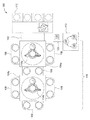
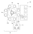
【解決手段】半導体処理用の処理システム100は、2つの移送チャンバ104a、104b、処理チャンバ108、及び回転モジュール106を含む。処理チャンバ108は、移送チャンバ104a、104bに連結される。回転モジュール106が、移送チャンバ104a、104b間に配置される。回転モジュール106は、基板を回転させるように構成される。移送チャンバ104a、104bは、処理チャンバ108と移送チャンバ104a、104bの間で基板を移送するように構成される。
【選択図】図1
Description
104a チャンバ
104b チャンバ
106 チャンバ
108 チャンバ
110 ロードロックチャンバ
112 ファクトリインターフェース
113 コントローラ
114a ロボット
114b ロボット
116 真空気密プラットフォーム
118 ポンプシステム
120 通信ケーブル
122 CPU
124 メモリ
126 サポート回路
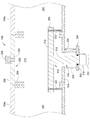
202 チャンバ本体
204 側壁
206 天井
210 内部容積
212 基板支持体アセンブリ
214 基板受取り面
216 シャフト
218 回転アクチュエータ
220 垂直アクチュエータ
222 リフトピン
223 回転センサ
224 開口
226 ベローズ
228 測定デバイス
230 窓
280 内部容積
282 内部容積
290 プラットフォーム
292 シャフトシール
294 プレート
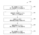
400 方法
402 ブロック
404 ブロック
406 ブロック
408 ブロック
410 ブロック
501 基板
550 ロボットブレード
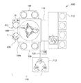
600 処理システム
606 回転モジュール
612 基板支持体アセンブリ
690 プラットフォーム
700 処理システム
706 回転モジュール
Claims (15)
- 半導体処理用の処理チャンバであって、
2つの移送チャンバと、
前記2つの移送チャンバの1つに連結された処理チャンバと、
前記移送チャンバ間に配置された回転モジュールであって、基板を回転させるように構成された回転モジュールと
を備える、処理チャンバ。 - 半導体処理用の処理チャンバであって、
移送チャンバと、
前記移送チャンバに連結された処理チャンバと、
前記移送チャンバに連結された回転モジュールであって、基板の一部が前記移送チャンバ内に残っている間に前記基板を回転させるように構成された回転モジュールと
を備える、処理チャンバ。 - 前記回転モジュールが、
内部容積を画定するチャンバ本体と、
前記内部容積内に配置された基板支持アセンブリと、
前記基板支持アセンブリに連結された回転アクチュエータであって、前記基板支持アセンブリを回転させるように構成された回転アクチュエータと
を備える、請求項1又は2に記載の処理システム。 - 前記回転モジュールが、
前記回転アクチュエータと通信する回転センサであって、前記基板支持アセンブリの回転を測定するように構成された回転センサを、
更に備える、請求項3に記載の処理システム。 - 前記回転モジュールが、
前記基板支持アセンブリに連結された垂直アクチュエータであって、前記基板支持アセンブリを垂直に移動させるように構成された垂直アクチュエータを、
更に備える、請求項3に記載の処理システム。 - 前記回転モジュールが、
前記チャンバ本体に連結された測定モジュールであって、基板上に堆積された膜の誘電特性を、前記チャンバ本体に形成された窓を通って検出するように構成されている測定モジュールを、
更に備える、請求項3に記載の処理システム。 - 前記基板支持アセンブリが、前記回転モジュールの前記内部容積の中に完全に包含される、請求項3に記載の処理システム。
- 前記基板支持アセンブリが、第一の移送チャンバの内部容積及び第二の移送チャンバの内部容積の中に部分的に延在する、請求項3に記載の処理システム。
- 基板を処理する方法であって、
処理チャンバ内で基板上に膜の第一の部分を堆積させることと、
前記基板を回転モジュールに移送することと、
前記基板を既定の量だけ回転させることと、
前記基板を処理チャンバに移送することと、
前記処理チャンバ内で前記基板上に前記膜の第二の部分を堆積させることと
を含む方法。 - 前記処理チャンバ内で基板支持アセンブリをZ方向下方に作動させることと、
前記処理チャンバ内で前記基板支持アセンブリ上に前記基板を位置決めすることであって、前記処理チャンバは、前記基板上に前記膜の前記第一の部分を堆積させるように構成されている、位置決めすることと、
前記処理チャンバ内で前記基板支持アセンブリをZ方向上方に作動させることと
を更に含む、請求項9に記載の方法。 - 前記基板が、前記処理チャンバから前記回転モジュールへ移送チャンバを通って移送される、請求項9に記載の方法。
- 前記基板が、前記移送チャンバの中に部分的に延在する基板支持アセンブリ上に位置決めされる、請求項11に記載の方法。
- 前記基板が180°回転される、請求項9に記載の方法。
- 前記基板が、n回回転され、n回の堆積を経る、請求項9に記載の方法。
- 前記基板が、4回回転され、4回の堆積を経る、請求項9に記載の方法。
Priority Applications (2)
| Application Number | Priority Date | Filing Date | Title |
|---|---|---|---|
| JP2021172093A JP7350035B2 (ja) | 2015-04-23 | 2021-10-21 | 半導体処理システムにおける外部基板回転 |
| JP2023147337A JP7680509B2 (ja) | 2015-04-23 | 2023-09-12 | 半導体処理システムにおける外部基板回転 |
Applications Claiming Priority (2)
| Application Number | Priority Date | Filing Date | Title |
|---|---|---|---|
| US201562151799P | 2015-04-23 | 2015-04-23 | |
| US62/151,799 | 2015-04-23 |
Related Child Applications (1)
| Application Number | Title | Priority Date | Filing Date |
|---|---|---|---|
| JP2021172093A Division JP7350035B2 (ja) | 2015-04-23 | 2021-10-21 | 半導体処理システムにおける外部基板回転 |
Publications (2)
| Publication Number | Publication Date |
|---|---|
| JP2017005242A true JP2017005242A (ja) | 2017-01-05 |
| JP6966181B2 JP6966181B2 (ja) | 2021-11-10 |
Family
ID=57147999
Family Applications (3)
| Application Number | Title | Priority Date | Filing Date |
|---|---|---|---|
| JP2016084118A Active JP6966181B2 (ja) | 2015-04-23 | 2016-04-20 | 半導体処理システムにおける外部基板回転 |
| JP2021172093A Active JP7350035B2 (ja) | 2015-04-23 | 2021-10-21 | 半導体処理システムにおける外部基板回転 |
| JP2023147337A Active JP7680509B2 (ja) | 2015-04-23 | 2023-09-12 | 半導体処理システムにおける外部基板回転 |
Family Applications After (2)
| Application Number | Title | Priority Date | Filing Date |
|---|---|---|---|
| JP2021172093A Active JP7350035B2 (ja) | 2015-04-23 | 2021-10-21 | 半導体処理システムにおける外部基板回転 |
| JP2023147337A Active JP7680509B2 (ja) | 2015-04-23 | 2023-09-12 | 半導体処理システムにおける外部基板回転 |
Country Status (5)
| Country | Link |
|---|---|
| US (3) | US10431480B2 (ja) |
| JP (3) | JP6966181B2 (ja) |
| KR (3) | KR102543643B1 (ja) |
| CN (3) | CN113611594B (ja) |
| TW (1) | TWI677046B (ja) |
Cited By (2)
| Publication number | Priority date | Publication date | Assignee | Title |
|---|---|---|---|---|
| JP2022517361A (ja) * | 2019-01-16 | 2022-03-08 | アプライド マテリアルズ インコーポレイテッド | 光学積層体の堆積及び装置内計測 |
| JP2022104056A (ja) * | 2020-12-28 | 2022-07-08 | 東京エレクトロン株式会社 | 搬送装置 |
Families Citing this family (15)
| Publication number | Priority date | Publication date | Assignee | Title |
|---|---|---|---|---|
| TWI677046B (zh) * | 2015-04-23 | 2019-11-11 | 美商應用材料股份有限公司 | 半導體處理系統中的外部基板材旋轉 |
| US10249525B2 (en) * | 2016-10-03 | 2019-04-02 | Applied Materials, Inc. | Dynamic leveling process heater lift |
| US10186449B2 (en) * | 2016-12-31 | 2019-01-22 | Applied Materials, Inc. | Apparatus and methods for wafer rotation to improve spatial ALD process uniformity |
| CN117524976A (zh) * | 2017-05-13 | 2024-02-06 | 应用材料公司 | 用于高质量间隙填充方案的循环可流动沉积和高密度等离子体处理处理 |
| CN111902929B (zh) * | 2018-03-09 | 2025-09-19 | 应用材料公司 | 用于含金属材料的高压退火处理 |
| SG11202009105YA (en) * | 2018-03-20 | 2020-10-29 | Tokyo Electron Ltd | Self-aware and correcting heterogenous platform incorporating integrated semiconductor processing modules and method for using same |
| US11499666B2 (en) * | 2018-05-25 | 2022-11-15 | Applied Materials, Inc. | Precision dynamic leveling mechanism with long motion capability |
| KR20200000638A (ko) * | 2018-06-25 | 2020-01-03 | 주성엔지니어링(주) | 기판 처리 장치 및 기판 처리 방법 |
| SG11202101649WA (en) * | 2018-09-28 | 2021-04-29 | Applied Materials Inc | Coaxial lift device with dynamic leveling |
| TWI696224B (zh) * | 2018-10-08 | 2020-06-11 | 馗鼎奈米科技股份有限公司 | 真空製程設備與真空製程方法 |
| CN113261075A (zh) * | 2018-12-21 | 2021-08-13 | 应用材料公司 | 用于形成触点的处理系统和方法 |
| WO2020211084A1 (en) * | 2019-04-19 | 2020-10-22 | Applied Materials, Inc. | Methods of forming a metal containing material |
| CN111235543B (zh) * | 2020-01-21 | 2022-03-15 | 南京京东方显示技术有限公司 | 一种真空腔旋转角度异常的校正装置及方法 |
| US12131934B2 (en) * | 2020-10-05 | 2024-10-29 | Applied Materials, Inc. | Semiconductor substrate support leveling apparatus |
| WO2023164228A1 (en) * | 2022-02-28 | 2023-08-31 | Applied Materials, Inc. | Crossflow deposition with substrate rotation for enhanced deposition uniformity |
Citations (6)
| Publication number | Priority date | Publication date | Assignee | Title |
|---|---|---|---|---|
| JP2002324829A (ja) * | 2001-07-13 | 2002-11-08 | Tokyo Electron Ltd | 処理システム |
| JP2005259902A (ja) * | 2004-03-10 | 2005-09-22 | Hitachi Kokusai Electric Inc | 基板処理装置 |
| JP2005328081A (ja) * | 2005-07-12 | 2005-11-24 | Hitachi Kokusai Electric Inc | 基板処理装置および半導体装置の製造方法 |
| WO2006137476A1 (ja) * | 2005-06-24 | 2006-12-28 | Ulvac, Inc. | 位置修正装置、真空処理装置、及び位置修正方法 |
| JP2009543355A (ja) * | 2006-07-03 | 2009-12-03 | アプライド マテリアルズ インコーポレイテッド | 進歩型フロントエンド処理のためのクラスターツール |
| JP2010206025A (ja) * | 2009-03-04 | 2010-09-16 | Tokyo Electron Ltd | 成膜装置、成膜方法、プログラム、およびコンピュータ可読記憶媒体 |
Family Cites Families (38)
| Publication number | Priority date | Publication date | Assignee | Title |
|---|---|---|---|---|
| US5135349A (en) * | 1990-05-17 | 1992-08-04 | Cybeq Systems, Inc. | Robotic handling system |
| IL99823A0 (en) * | 1990-11-16 | 1992-08-18 | Orbot Instr Ltd | Optical inspection method and apparatus |
| KR0165484B1 (ko) * | 1995-11-28 | 1999-02-01 | 김광호 | 탄탈륨산화막 증착 형성방법 및 그 장치 |
| KR19980029384A (ko) * | 1996-10-25 | 1998-07-25 | 김광호 | 반도체 소자 제조 장치 |
| US7619752B2 (en) * | 2000-03-21 | 2009-11-17 | J. A. Woollam Co., Inc. | Sample orientation system and method |
| JP4849705B2 (ja) * | 2000-03-24 | 2012-01-11 | 東京エレクトロン株式会社 | プラズマ処理装置、プラズマ生成導入部材及び誘電体 |
| US6660660B2 (en) * | 2000-10-10 | 2003-12-09 | Asm International, Nv. | Methods for making a dielectric stack in an integrated circuit |
| JP2002124478A (ja) | 2000-10-18 | 2002-04-26 | Nec Kyushu Ltd | 常圧cvd装置 |
| JP4467761B2 (ja) | 2000-11-07 | 2010-05-26 | 株式会社アルバック | 基板の処理装置及び基板の処理方法 |
| AU2003259203A1 (en) * | 2002-07-22 | 2004-02-09 | Brooks Automation, Inc. | Substrate processing apparatus |
| US20050223837A1 (en) * | 2003-11-10 | 2005-10-13 | Blueshift Technologies, Inc. | Methods and systems for driving robotic components of a semiconductor handling system |
| US7458763B2 (en) * | 2003-11-10 | 2008-12-02 | Blueshift Technologies, Inc. | Mid-entry load lock for semiconductor handling system |
| TWI355298B (en) * | 2004-01-26 | 2012-01-01 | Applied Materials Inc | Apparatus for electroless deposition of metals ont |
| JP2006028577A (ja) * | 2004-07-15 | 2006-02-02 | Canon Anelva Corp | Cvd装置 |
| US20070134821A1 (en) * | 2004-11-22 | 2007-06-14 | Randhir Thakur | Cluster tool for advanced front-end processing |
| US20060281310A1 (en) * | 2005-06-08 | 2006-12-14 | Applied Materials, Inc. | Rotating substrate support and methods of use |
| JP2007005435A (ja) * | 2005-06-22 | 2007-01-11 | Rorze Corp | 処理装置 |
| JP4753644B2 (ja) | 2005-07-05 | 2011-08-24 | 積水化学工業株式会社 | 常圧cvd方法及び装置 |
| TW200715448A (en) * | 2005-07-25 | 2007-04-16 | Canon Anelva Corp | Vacuum processing apparatus, semiconductor device manufacturing method and semiconductor device manufacturing system |
| US7534080B2 (en) * | 2005-08-26 | 2009-05-19 | Ascentool, Inc. | Vacuum processing and transfer system |
| KR20080004118A (ko) * | 2006-07-04 | 2008-01-09 | 피에스케이 주식회사 | 기판 처리 설비 |
| US20080041716A1 (en) * | 2006-08-18 | 2008-02-21 | Schott Lithotec Usa Corporation | Methods for producing photomask blanks, cluster tool apparatus for producing photomask blanks and the resulting photomask blanks from such methods and apparatus |
| US20080219810A1 (en) * | 2007-03-05 | 2008-09-11 | Van Der Meulen Peter | Semiconductor manufacturing process modules |
| US8057602B2 (en) * | 2007-05-09 | 2011-11-15 | Applied Materials, Inc. | Apparatus and method for supporting, positioning and rotating a substrate in a processing chamber |
| KR100915797B1 (ko) * | 2007-09-20 | 2009-09-08 | 주식회사 에이디피엔지니어링 | 기판처리장치 및 기판처리장치 내부의 공정공간을 개폐하는방법 |
| US20090120368A1 (en) * | 2007-11-08 | 2009-05-14 | Applied Materials, Inc. | Rotating temperature controlled substrate pedestal for film uniformity |
| KR100965413B1 (ko) * | 2008-04-18 | 2010-06-25 | 엘아이지에이디피 주식회사 | 기판 처리용 클러스터 장치 및 클러스터 장치의 기판 처리방법 |
| US20100227059A1 (en) | 2009-03-04 | 2010-09-09 | Tokyo Electron Limited | Film deposition apparatus, film deposition method, and computer readable storage medium |
| JP5181100B2 (ja) | 2009-04-09 | 2013-04-10 | 東京エレクトロン株式会社 | 基板処理装置、基板処理方法及び記憶媒体 |
| CN101956173B (zh) * | 2009-07-20 | 2013-06-05 | 鸿富锦精密工业(深圳)有限公司 | 使用承载组件的镀膜装置 |
| US9512520B2 (en) * | 2011-04-25 | 2016-12-06 | Applied Materials, Inc. | Semiconductor substrate processing system |
| US9748077B2 (en) * | 2012-05-29 | 2017-08-29 | Jusung Engineering Co., Ltd. | Substrate processing device and substrate processing method |
| JP5993625B2 (ja) * | 2012-06-15 | 2016-09-14 | 株式会社Screenホールディングス | 基板反転装置、および、基板処理装置 |
| JP6160614B2 (ja) * | 2012-07-04 | 2017-07-12 | 東京エレクトロン株式会社 | 基板処理装置 |
| KR102449103B1 (ko) | 2014-03-12 | 2022-09-28 | 어플라이드 머티어리얼스, 인코포레이티드 | 반도체 챔버에서의 웨이퍼 회전 |
| US10236197B2 (en) | 2014-11-06 | 2019-03-19 | Applied Materials, Inc. | Processing system containing an isolation region separating a deposition chamber from a treatment chamber |
| TWI677046B (zh) * | 2015-04-23 | 2019-11-11 | 美商應用材料股份有限公司 | 半導體處理系統中的外部基板材旋轉 |
| JP7525394B2 (ja) * | 2020-12-28 | 2024-07-30 | 東京エレクトロン株式会社 | 搬送装置 |
-
2016
- 2016-03-31 TW TW105110319A patent/TWI677046B/zh active
- 2016-04-05 US US15/091,260 patent/US10431480B2/en active Active
- 2016-04-20 CN CN202110890839.7A patent/CN113611594B/zh active Active
- 2016-04-20 JP JP2016084118A patent/JP6966181B2/ja active Active
- 2016-04-20 CN CN201620335567.9U patent/CN205954106U/zh not_active Expired - Fee Related
- 2016-04-20 CN CN201610248104.3A patent/CN106067433B/zh active Active
- 2016-04-22 KR KR1020160049510A patent/KR102543643B1/ko active Active
-
2019
- 2019-09-30 US US16/588,959 patent/US11574825B2/en active Active
-
2021
- 2021-10-21 JP JP2021172093A patent/JP7350035B2/ja active Active
-
2023
- 2023-01-26 US US18/101,995 patent/US12581896B2/en active Active
- 2023-06-08 KR KR1020230073432A patent/KR102713230B1/ko active Active
- 2023-09-12 JP JP2023147337A patent/JP7680509B2/ja active Active
-
2024
- 2024-09-26 KR KR1020240130551A patent/KR102920685B1/ko active Active
Patent Citations (6)
| Publication number | Priority date | Publication date | Assignee | Title |
|---|---|---|---|---|
| JP2002324829A (ja) * | 2001-07-13 | 2002-11-08 | Tokyo Electron Ltd | 処理システム |
| JP2005259902A (ja) * | 2004-03-10 | 2005-09-22 | Hitachi Kokusai Electric Inc | 基板処理装置 |
| WO2006137476A1 (ja) * | 2005-06-24 | 2006-12-28 | Ulvac, Inc. | 位置修正装置、真空処理装置、及び位置修正方法 |
| JP2005328081A (ja) * | 2005-07-12 | 2005-11-24 | Hitachi Kokusai Electric Inc | 基板処理装置および半導体装置の製造方法 |
| JP2009543355A (ja) * | 2006-07-03 | 2009-12-03 | アプライド マテリアルズ インコーポレイテッド | 進歩型フロントエンド処理のためのクラスターツール |
| JP2010206025A (ja) * | 2009-03-04 | 2010-09-16 | Tokyo Electron Ltd | 成膜装置、成膜方法、プログラム、およびコンピュータ可読記憶媒体 |
Cited By (9)
| Publication number | Priority date | Publication date | Assignee | Title |
|---|---|---|---|---|
| JP2022517361A (ja) * | 2019-01-16 | 2022-03-08 | アプライド マテリアルズ インコーポレイテッド | 光学積層体の堆積及び装置内計測 |
| JP7447126B2 (ja) | 2019-01-16 | 2024-03-11 | アプライド マテリアルズ インコーポレイテッド | 光学積層体の堆積及び装置内計測 |
| TWI844584B (zh) * | 2019-01-16 | 2024-06-11 | 美商應用材料股份有限公司 | 光學堆疊沉積與機載量測法 |
| TWI882794B (zh) * | 2019-01-16 | 2025-05-01 | 美商應用材料股份有限公司 | 光學堆疊沉積與機載量測法 |
| JP2022104056A (ja) * | 2020-12-28 | 2022-07-08 | 東京エレクトロン株式会社 | 搬送装置 |
| JP7525394B2 (ja) | 2020-12-28 | 2024-07-30 | 東京エレクトロン株式会社 | 搬送装置 |
| JP2024133281A (ja) * | 2020-12-28 | 2024-10-01 | 東京エレクトロン株式会社 | 搬送装置 |
| US12476121B2 (en) | 2020-12-28 | 2025-11-18 | Tokyo Electron Limited | Transfer apparatus |
| KR102941975B1 (ko) * | 2020-12-28 | 2026-03-19 | 도쿄엘렉트론가부시키가이샤 | 반송 장치 |
Also Published As
| Publication number | Publication date |
|---|---|
| JP7680509B2 (ja) | 2025-05-20 |
| KR102543643B1 (ko) | 2023-06-13 |
| KR102920685B1 (ko) | 2026-01-29 |
| CN106067433A (zh) | 2016-11-02 |
| CN205954106U (zh) | 2017-02-15 |
| KR102713230B1 (ko) | 2024-10-02 |
| US10431480B2 (en) | 2019-10-01 |
| CN106067433B (zh) | 2021-07-27 |
| US12581896B2 (en) | 2026-03-17 |
| US20160315000A1 (en) | 2016-10-27 |
| TW201642380A (zh) | 2016-12-01 |
| TWI677046B (zh) | 2019-11-11 |
| KR20240144879A (ko) | 2024-10-04 |
| US11574825B2 (en) | 2023-02-07 |
| JP2022023889A (ja) | 2022-02-08 |
| KR20160126914A (ko) | 2016-11-02 |
| JP2023175774A (ja) | 2023-12-12 |
| US20230162999A1 (en) | 2023-05-25 |
| JP6966181B2 (ja) | 2021-11-10 |
| CN113611594B (zh) | 2025-08-22 |
| JP7350035B2 (ja) | 2023-09-25 |
| CN113611594A (zh) | 2021-11-05 |
| KR20230087431A (ko) | 2023-06-16 |
| US20200035522A1 (en) | 2020-01-30 |
Similar Documents
| Publication | Publication Date | Title |
|---|---|---|
| JP7680509B2 (ja) | 半導体処理システムにおける外部基板回転 | |
| US11408070B2 (en) | Wafer processing apparatus and wafer processing method | |
| TWI838131B (zh) | 對於旋轉晶圓之處理模組之處理站的自動校正 | |
| US10777439B1 (en) | Substrate processing apparatus | |
| US9929008B2 (en) | Substrate processing method and substrate processing apparatus | |
| US20190093230A1 (en) | Substrate Processing Method and Substrate Processing Apparatus | |
| CN107546123A (zh) | 基板处理单元、烘焙装置及基板处理方法 | |
| US11784070B2 (en) | Heat treatment apparatus, heat treatment method, and film forming method | |
| US20260033276A1 (en) | Substrate Processing Apparatus, Method of Manufacturing Semiconductor Device and Method of Processing Substrate Support | |
| JP6584350B2 (ja) | 制御装置、基板処理システム、基板処理方法及びプログラム | |
| US20180258528A1 (en) | Substrate processing apparatus | |
| JP7296739B2 (ja) | 処理装置及び処理装置の動作方法 | |
| US11359732B1 (en) | Method and mechanism for symmetrically controlling pressure in process chamber | |
| JP6308030B2 (ja) | 成膜装置、成膜方法及び記憶媒体 |
Legal Events
| Date | Code | Title | Description |
|---|---|---|---|
| A621 | Written request for application examination |
Free format text: JAPANESE INTERMEDIATE CODE: A621 Effective date: 20190416 |
|
| A977 | Report on retrieval |
Free format text: JAPANESE INTERMEDIATE CODE: A971007 Effective date: 20200518 |
|
| A131 | Notification of reasons for refusal |
Free format text: JAPANESE INTERMEDIATE CODE: A131 Effective date: 20200623 |
|
| A521 | Request for written amendment filed |
Free format text: JAPANESE INTERMEDIATE CODE: A523 Effective date: 20200918 |
|
| A131 | Notification of reasons for refusal |
Free format text: JAPANESE INTERMEDIATE CODE: A131 Effective date: 20210209 |
|
| A521 | Request for written amendment filed |
Free format text: JAPANESE INTERMEDIATE CODE: A523 Effective date: 20210507 |
|
| TRDD | Decision of grant or rejection written | ||
| A01 | Written decision to grant a patent or to grant a registration (utility model) |
Free format text: JAPANESE INTERMEDIATE CODE: A01 Effective date: 20210824 |
|
| A601 | Written request for extension of time |
Free format text: JAPANESE INTERMEDIATE CODE: A601 Effective date: 20210924 |
|
| A61 | First payment of annual fees (during grant procedure) |
Free format text: JAPANESE INTERMEDIATE CODE: A61 Effective date: 20211021 |
|
| R150 | Certificate of patent or registration of utility model |
Ref document number: 6966181 Country of ref document: JP Free format text: JAPANESE INTERMEDIATE CODE: R150 |
|
| R250 | Receipt of annual fees |
Free format text: JAPANESE INTERMEDIATE CODE: R250 |